TMPM4G Group(1)
Datasheet
CMOS Digital Integrated Circuit Silicon Monolithic
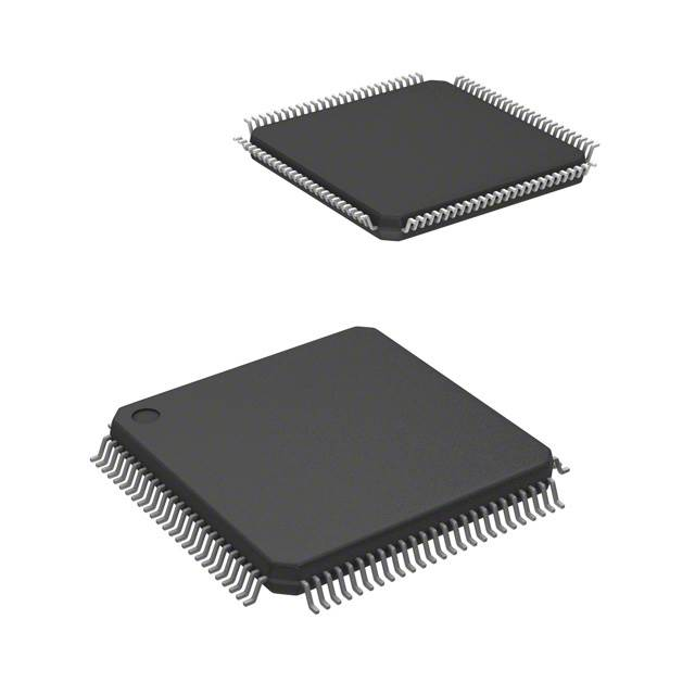
LQFP176(20x20mm, 0.4mm pitch)
TMPM4G Group(1)
LQFP144(20x20mm, 0.5mm pitch)
LQFP128(14x14mm, 0.4mm pitch)
LQFP100(14x14mm, 0.5mm pitch)
General Description
VFBGA177(13x13mm, 0.8mm pitch)
VFBGA145(12x12mm, 0.8mm pitch)
●
Arm ® Cortex®-M4( with FPU)
●
Frequency: 1 to 160 MHz, Operation voltage: 2.7 to 3.6 V
●
Code Flash: 512 KB to 1536 KB. Data Flash: 32KB
●
Built-in High speed 12-bit AD converter and plenty of timers/serial channels
Applications
TMPM4G group(1) integrates widely used for the equipment in which high speed data procedure is
required, such as OA/digital products, industrial equipment, and others.
Features
● Arm Cortex-M4( with FPU)
● I/O ports: 87 to 155 (Input: 4, Output: 1)
‒ Operation frequency: 1 to 160 MHz
‒ Enable to select Pull-up/Pull-down resistor, Open-drain
‒ Memory Protection Unit (MPU)
‒ 5V tolerant, 3V tolerant
● Supply voltage and power consumption
‒ Operation voltage:
● On-chip debug (JTAG/SW) and NBDIF (RAM monitor)
2.7 to 3.6 V
● Trigger Selector (TRGSEL)
‒ Low-power consumption operation: IDLE, STOP1, and STOP2
‒ Expand trigger requests for DMA Controller, Timer counter, and
● Operation temperature:
others.
- 40 to +85℃@operation frequency 1 to 120 MHz
● DMA Controller: 3 units
- 40 to +70℃@operation frequency 1 to 160 MHz
‒ MDMAC: 1 unit,
● Internal memory
DMA requests: 30 to 32 factors, internal/external triggers
‒ Code Flash: 512 KB to 1536 KB, rewritable up to 10,000 times
‒ HDMAC: 2 units,
‒ Data Flash: 32 KB, rewritable up to 100,000 times
DMA requests: 13 to 15 factors, internal/external triggers
‒ Data Flash is rewritable during instruction execution
● External bus interface(EBIF)
‒ RAM: 128 KB to 192 KB and Backup RAM: 2 KB (all products)
‒ Expandable to 64MB(Program/data)
● Clock
‒ External data bus(separate bug/multiplexed bun): 8/16 bit width
‒ External high speed oscillator: 8 MHz to 20 MHz (Ceramic and
‒ Chip select controller: 4 channels
Crystal)
● Asynchronous serial communication
‒ External high speed clock input: 8 to 20 MHz
‒ UART: 3 to 6 channels, 5.0 Mbps (Max). FIFO (Transmission
‒ Internal high speed oscillator1 (IHOSC1):10MHz, user trimming
8 stage and Reception 8 stage)
function
‒ FUART: 1 or 2 channels, 2.5Mbps (Max). FIFO (Transmission
‒ Internal high speed oscillator2 (IHOSC2):10MHz
‒ PLL: 160 MHz output
32 stage and Reception 32 stage) and IrDA 115.2Kbps (Max).
● Serial Peripheral Interface (TSPI): 5 to 9 channels
‒ External low speed oscillator: 32.768 kHz
‒ SIO/SPI mode, 25 Mbps (Max)
● Oscillation Frequency Detectior (OFD): Abnormal system clock
‒ FIFO (Transmission 16bit x 8 stage and Reception 16bit x 8
detection
● Voltage Detection (LVD): 7 levels. selection between interrupts
and reset outputs
● Interrupt
‒ External: 12 to 16 factors. Integrate digital noise filters (DNF).
‒ Internal: 91 to 124 factors
stage)
●
I2C
Interface (I2C):
3 to 5 channels
Multi master, standard mode/fast mode available
● Serial Memory Interface (SMIF): 1 channel
‒ Connectable to two SPI FLASH
Start of commercial production
2019-2
2019-03-26
1 / 132
Rev.4.2
© 2018-2019
Toshiba Electronic Devices & Storage Corporation
�TMPM4G Group(1)
Datasheet
● Consumer Electronics Control Circuit (CEC): 1 channel
● 8-bit DA converter (DAC): 2 channels
● 12-bit AD converter (ADC): 16 to 24 channel inputs
‒ Sample and hold circuit
‒ Conversion time: 1.0 µs @fADCLK = 60 MHz
● Advanced Programmable Motor Control Circuit (A-PMD): 1 channel
‒ 3 phase PWM output, Synchronized with 12-bit ADC
‒ Emergency stop function by external inputs (EMG0 pin and
OVV0 pin)
● 32-bit Timer Event Counter (T32A)
‒ 28 channels as 16-bit Timers:14 channels as 32-bit Timers
‒ Interval Timer, event counter, input capture, phase difference
input, PPG output, Sync Start,Trigger Start
● Interval Sensor Detection circuit (ISD): 3 units
‒ 4 inputs per unit
‒ Sampling 12 inputs at maximum simultaneously in Unit
synchronous mode
‒ Low speed oscillator (32.768 kHz) and 32-bit timer output can
be used as sampling clock
● Long Term Timer (LTTMR): 1 channel
‒ Interval time of 0.1μs to 6553.5μs can be set
● Real-time Clock (RTC): 1 channel
● Clock Selective Watchdog Timer (SIWDT): 1 channel
‒ Clocks other than the system clock can be selected.
‒ Clear window, interrupts and reset outputs
● Remote Control Signal Preprocessor (RMC): 1 to 2channels
● Supports boundary scan(BSC)
2019-03-26
2 / 132
Rev.4.2
�TMPM4G Group(1)
Datasheet
Products Lists Categorized by Functions
The product under development is contained in this table.
For the newest status of each product, Please contact your sales representative.
Table 1 TMPM4G9 (1)
TMPM4G9F15FG
TMPM4G9F10FG
TMPM4G9FEFG
TMPM4G9FDFG
Code Flash (KB)
1536
1024
768
512
Data Flash (KB)
32
32
32
32
RAM (KB)
192
192
128
128
2
2
2
2
Built-in Functions
Memory
Backup RAM (KB)
I/O port
PORT (pin)
155
155
155
155
External interrupt
INT
16
16
16
16
External bus
EBIF
Sep./Mul.
Sep./Mul.
Sep./Mul.
Sep./Mul.
MDMAC (ch)
32
32
32
32
HDMAC (ch)
15
15
15
15
T32A (ch)
14
14
14
14
LTTMR (ch)
1
1
1
1
RTC (ch)
1
1
1
1
UART(ch)
6
6
6
6
FUART(ch)
2
2
2
2
Serial communication
I2C(ch)
5
5
5
5
function
TSPI(ch)
9
9
9
9
SMIF(ch)
1
1
1
1
CEC (ch)
1
1
1
1
12-bit ADC (ch)
24
24
24
24
8-bit DAC (ch)
2
2
2
2
A-PMD (ch)
1
1
1
1
RMC (ch)
2
2
2
2
ISD (unit)
3
3
3
3
LVD(ch)
1
1
1
1
SIWDT(ch)
1
1
1
1
OFD(ch)
1
1
1
1
POR
1
1
1
1
On-chip debug
On-chip debug
On-chip debug
On-chip debug
(JTAG/SW)
(JTAG/SW)
(JTAG/SW)
(JTAG/SW)
TRACE(4bits)
TRACE(4bits)
TRACE(4bits)
TRACE(4bits)
NBDIF
NBDIF
NBDIF
NBDIF
DMAC
Timer function
Analog function
Motor control function
Remote Control
preprocessor peripherals
Interval Sensor
Detection peripherals
System function
Debug interface
Package
2019-03-26
Debug
LQFP176
Package type
(20 mm x 20 mm, 0.4 mm pitch)
3 / 132
Rev.4.2
�TMPM4G Group(1)
Datasheet
Table 2 TMPM4G9 (2)
Built-in Functions
Memory
TMPM4G9F15XBG
TMPM4G9F10XBG
TMPM4G9FEXBG
TMPM4G9FDXBG
Code Flash (KB)
1536
1024
768
512
Data Flash (KB)
32
32
32
32
RAM (KB)
192
192
128
128
2
2
2
2
Backup RAM (KB)
I/O port
PORT (pin)
155
155
155
155
External interrupt
INT
16
16
16
16
External bus
EBIF
Sep./Mul.
Sep./Mul.
Sep./Mul.
Sep./Mul.
MDMAC (ch)
32
32
32
32
HDMAC (ch)
15
15
15
15
T32A (ch)
14
14
14
14
LTTMR (ch)
1
1
1
1
RTC (ch)
1
1
1
1
UART (ch)
6
6
6
6
FUART (ch)
2
2
2
2
Serial communication
I2C (ch)
5
5
5
5
function
TSPI (ch)
9
9
9
9
SMIF (ch)
1
1
1
1
CEC (ch)
1
1
1
1
12-bit ADC (ch)
24
24
24
24
8-bit DAC (ch)
2
2
2
2
A-PMD (ch)
1
1
1
1
RMC (ch)
2
2
2
2
ISD (unit)
3
3
3
3
LVD (ch)
1
1
1
1
SIWDT (ch)
1
1
1
1
OFD (ch)
1
1
1
1
POR
1
1
1
1
On-chip debug
On-chip debug
On-chip debug
On-chip debug
DMAC
Timer function
Analog function
Motor control function
Remote Control
preprocessor peripherals
Interval Sensor
Detection peripherals
System function
Debug interface
Package
2019-03-26
Debug
(JTAG/SW)
(JTAG/SW)
(JTAG/SW)
(JTAG/SW)
TRACE(4bits)
TRACE(4bits)
TRACE(4bits)
TRACE(4bits)
NBDIF
NBDIF
NBDIF
NBDIF
VFBGA177
Package type
(13 mm x 13 mm, 0.8 mm pitch)
4 / 132
Rev.4.2
�TMPM4G Group(1)
Datasheet
Table 3 TMPM4G8 (1)
TMPM4G8F15FG
TMPM4G8F10FG
TMPM4G8FEFG
TMPM4G8FDFG
Code Flash (KB)
1536
1024
768
512
Data Flash (KB)
32
32
32
32
RAM (KB)
192
192
128
128
2
2
2
2
Built-in Functions
Memory
Backup RAM (KB)
I/O port
PORT (pin)
127
127
127
127
External interrupt
INT
16
16
16
16
External bus
EBIF
Sep./Mul.
Sep./Mul.
Sep./Mul.
Sep./Mul.
MDMAC (ch)
32
32
32
32
HDMAC (ch)
15
15
15
15
T32A (ch)
14
14
14
14
LTTMR (ch)
1
1
1
1
RTC (ch)
1
1
1
1
UART(ch)
5
5
5
5
FUART(ch)
2
2
2
2
Serial communication
I2C(ch)
5
5
5
5
function
TSPI(ch)
8
8
8
8
SMIF(ch)
1
1
1
1
CEC(ch)
1
1
1
1
12-bit ADC(ch)
24
24
24
24
8-bit DAC(ch)
2
2
2
2
A-PMD(ch)
1
1
1
1
RMC(ch)
2
2
2
2
ISD(unit)
2
2
2
2
LVD(ch)
1
1
1
1
SIWDT(ch)
1
1
1
1
OFD(ch)
1
1
1
1
POR
1
1
1
1
On-chip debug
On-chip debug
On-chip debug
On-chip debug
DMAC
Timer function
Analog function
Motor control function
Remote Control
preprocessor peripherals
Interval Sensor
Detection peripherals
System function
Debug interface
Package
2019-03-26
Debug
(JTAG/SW)
(JTAG/SW)
(JTAG/SW)
(JTAG/SW)
TRACE(4bits)
TRACE(4bits)
TRACE(4bits)
TRACE(4bits)
NBDIF
NBDIF
NBDIF
NBDIF
LQFP144
Package type
(20 mm x 20 mm, 0.5 mm pitch)
5 / 132
Rev.4.2
�TMPM4G Group(1)
Datasheet
Table 4 TMPM4G8 (2)
Built-in Functions
Memory
TMPM4G8F15XBG
TMPM4G8F10XBG
TMPM4G8FEXBG
TMPM4G8FDXBG
Code Flash (KB)
1536
1024
768
512
Data Flash (KB)
32
32
32
32
RAM (KB)
192
192
128
128
2
2
2
2
Backup RAM (KB)
I/O port
PORT (pin)
127
127
127
127
External interrupt
INT
16
16
16
16
External bus
EBIF
Sep./Mul.
Sep./Mul.
Sep./Mul.
Sep./Mul.
MDMAC (ch)
32
32
32
32
HDMAC (ch)
15
15
15
15
T32A (ch)
14
14
14
14
LTTMR (ch)
1
1
1
1
RTC (ch)
1
1
1
1
UART (ch)
5
5
5
5
FUART (ch)
2
2
2
2
Serial communication
I2C (ch)
5
5
5
5
function
TSPI (ch)
8
8
8
8
SMIF (ch)
1
1
1
1
CEC (ch)
1
1
1
1
12-bit ADC (ch)
24
24
24
24
8-bit DAC (ch)
2
2
2
2
A-PMD (ch)
1
1
1
1
RMC (ch)
2
2
2
2
ISD (unit)
2
2
2
2
LVD (ch)
1
1
1
1
SIWDT (ch)
1
1
1
1
OFD (ch)
1
1
1
1
POR
1
1
1
1
On-chip debug
On-chip debug
On-chip debug
On-chip debug
DMAC
Timer function
Analog function
Motor control function
Remote Control
preprocessor peripherals
Interval Sensor
Detection peripherals
System function
Debug interface
Package
2019-03-26
Debug
(JTAG/SW)
(JTAG/SW)
(JTAG/SW)
(JTAG/SW)
TRACE(4bits)
TRACE(4bits)
TRACE(4bits)
TRACE(4bits)
NBDIF
NBDIF
NBDIF
NBDIF
VFBGA145
Package type
(12 mm x 12 mm, 0.8 mm pitch)
6 / 132
Rev.4.2
�TMPM4G Group(1)
Datasheet
Table 5 TMPM4G7
TMPM4G7F10FG
TMPM4G7FEFG
TMPM4G7FDFG
Code Flash (KB)
1024
768
512
Data Flash (KB)
32
32
32
RAM (KB)
192
128
128
2
2
2
Built-in Functions
Memory
Backup RAM (KB)
I/O port
PORT (pin)
111
111
111
External interrupt
INT
14
14
14
External bus
EBIF
Sep./Mul.
Sep./Mul.
Sep./Mul.
MDMAC (ch)
30
30
30
HDMAC (ch)
15
15
15
T32A (ch)
14
14
14
LTTMR (ch)
1
1
1
RTC (ch)
1
1
1
UART(ch)
4
4
4
FUART(ch)
1
1
1
Serial communication
I2C (ch)
3
3
3
function
TSPI (ch)
6
6
6
SMIF (ch)
1
1
1
CEC (ch)
1
1
1
12-bit ADC (ch)
20
20
20
8-bit DAC (ch)
2
2
2
A-PMD(ch)
1
1
1
RMC(ch)
2
2
2
ISD(unit)
2
2
2
LVD(ch)
1
1
1
SIWDT(ch)
1
1
1
OFD(ch)
1
1
1
POR
1
1
1
On-chip debug
On-chip debug
On-chip debug
DMAC
Timer function
Analog function
Motor control function
Remote Control
preprocessor peripherals
Interval Sensor Detection
peripherals
System function
Debug interface
Debug
(JTAG/SW)
(JTAG/SW)
(JTAG/SW)
TRACE(4bits)
TRACE(4bits)
TRACE(4bits)
NBDIF
NBDIF
NBDIF
Package
2019-03-26
LQFP128
Package type
(14 mm x 14 mm, 0.4 mm pitch)
7 / 132
Rev.4.2
�TMPM4G Group(1)
Datasheet
Table 6 TMPM4G6
TMPM4G6F10FG
TMPM4G6FEFG
TMPM4G6FDFG
Code Flash (KB)
1024
768
512
Data Flash (KB)
32
32
32
RAM (KB)
192
128
128
Backup RAM (KB)
2
2
2
I/O port
PORT (pin)
91
91
91
External interrupt
INT
12
12
12
External bus
EBIF
Sep./Mul.
Sep./Mul.
Sep./Mul.
MDMAC (ch)
30
30
30
HDMAC (ch)
13
13
13
T32A (ch)
14
14
14
LTTMR (ch)
1
1
1
RTC (ch)
1
1
1
UART (ch)
3
3
3
FUART (ch)
1
1
1
Serial communication
I2C (ch)
3
3
3
function
TSPI (ch)
5
5
5
SMIF (ch)
1
1
1
CEC (ch)
1
1
1
12-bit ADC (ch)
16
16
16
8-bit DAC (ch)
2
2
2
A-PMD (ch)
1
1
1
RMC (ch)
1
1
1
ISD(unit)
1
1
1
LVD (ch)
1
1
1
SIWDT (ch)
1
1
1
OFD (ch)
1
1
1
POR
1
1
1
On-chip debug
On-chip debug
On-chip debug
Built-in Functions
Memory
DMAC
Timer function
Analog function
Motor control function
Remote Control
preprocessor peripherals
Interval Sensor Detection
peripherals
System function
Debug interface
Debug
(JTAG/SW)
(JTAG/SW)
(JTAG/SW)
TRACE(4bits)
TRACE(4bits)
TRACE(4bits)
NBDIF
NBDIF
NBDIF
Package
2019-03-26
LQFP100
Package type
(14 mm x 14 mm, 0.5 mm pitch)
8 / 132
Rev.4.2
�TMPM4G Group(1)
Datasheet
Contents
General Description.....................................................................................................................................1
Applications .................................................................................................................................................1
Features ......................................................................................................................................................1
Products Lists Categorized by Functions ................................................................................................3
Contents ......................................................................................................................................................9
List of Figures ........................................................................................................................................12
List of Tables .........................................................................................................................................13
Preface ......................................................................................................................................................15
Conventions ...........................................................................................................................................15
Terms and Abbreviations.......................................................................................................................17
1.
Block Diagram ....................................................................................................................................18
2.
Pin Assignment ..................................................................................................................................19
2.1. LQFP176 ........................................................................................................................................19
2.2. LQFP144 ........................................................................................................................................20
2.3. LQFP128 ........................................................................................................................................21
2.4. LQFP100 ........................................................................................................................................22
2.5. VFBGA177......................................................................................................................................23
2.6. VFBGA145......................................................................................................................................24
3.
Memory Map ......................................................................................................................................25
3.1. List of Memory Sizes ......................................................................................................................26
4.
Pin Description ...................................................................................................................................27
4.1. Functional Pin Name and Function ................................................................................................27
4.1.1. Peripheral Function Pins ................................................................................................................................. 27
4.1.2. Debug Pins ...................................................................................................................................................... 30
4.1.3. Control Pins ..................................................................................................................................................... 31
4.1.4. Power Supply Pins .......................................................................................................................................... 32
4.2. Functional Pin and Port Assignment (Pin Number) .......................................................................33
4.3. Ports ...............................................................................................................................................51
4.3.1. Port Specifications Table ................................................................................................................................. 52
5.
Functional Description and Operation Description ............................................................................57
5.1. Reference Manuals ........................................................................................................................57
5.2. Processor Core...............................................................................................................................58
5.2.1. Core Information .............................................................................................................................................. 58
5.2.2. Configurable Options ....................................................................................................................................... 58
5.3. Clock Control and Operation Mode (CG) .......................................................................................59
5.4. Flash Memory (Code FLASH, Data FLASH) .................................................................................59
5.5. Oscillation Circuit ............................................................................................................................60
5.6. Trimming Circuit (TRM) ..................................................................................................................60
2019-03-26
9 / 132
Rev.4.2
�TMPM4G Group(1)
Datasheet
5.7. Oscillation Frequency Detector (OFD) ...........................................................................................61
5.8. Voltage Detection Circuit (LVD) .....................................................................................................61
5.9. Digital Noise Filter Circuit (DNF) ....................................................................................................61
5.10. Debug Interface (DEBUG)............................................................................................................62
5.11. Non Break Debug Interface(NBDIF) ............................................................................................63
5.12. Interval Sensor Detection Circuit(ISD) .........................................................................................63
5.13. DMA Controller .............................................................................................................................64
5.13.1. Multi-Function DMA Controller (MDMAC) ...................................................................................................... 64
5.13.2. High Speed DMA Controller (HDMAC) .......................................................................................................... 64
5.14. External Bus Interface (EBIF).......................................................................................................65
5.15. Serial Memory Interface (SMIF) ...................................................................................................65
5.16. Asynchronous Serial Communication Circuit ...............................................................................66
5.16.1. Asynchronous Serial Communication Circuit (UART).................................................................................... 66
5.16.2. Full Universal Asynchronous Receiver Transmitter Circuit (FUART)............................................................. 66
5.17. Serial Peripheral Interface (TSPI) ................................................................................................67
5.18. I2C Interface (I2C) .........................................................................................................................67
5.19. Consumer Electronics Control Circuit (CEC) ...............................................................................68
5.20. 8-bit Digital to Analog Converter (DAC) .......................................................................................68
5.21. 12-bit Analog to Digital Converter (ADC) .....................................................................................68
5.22. Advanced Programmable Motor Control Circuit (A-PMD) ...........................................................69
5.23. 32-bit Timer Event Counter (T32A) ..............................................................................................69
5.24. Long Term Timer (LTTMR) ..........................................................................................................70
5.25. Real Time Clock (RTC) ................................................................................................................70
5.26. Clock Selective Watchdog Timer (SIWDT) ..................................................................................70
5.27. Remote Control Signal Preprocessor (RMC) ...............................................................................71
5.28. Boundary Scan (BSC) ..................................................................................................................71
6.
Equivalent Circuit ...............................................................................................................................72
6.1. Port .................................................................................................................................................72
6.2. Analog Power pin ...........................................................................................................................77
6.3. Control Pin ......................................................................................................................................77
6.4. Clock control ...................................................................................................................................78
7.
Electrical Characteristics....................................................................................................................79
7.1. Absolute Maximum Ratings............................................................................................................79
7.2. DC Electrical Characteristics (1/2) .................................................................................................80
7.3. DC Electrical Characteristics (2/2) (Consumption current) ............................................................84
7.4. 12-bit AD Converter Characteristics...............................................................................................86
7.5. 8-bit DA Converter Characteristics .................................................................................................86
7.6. Characteristics of Internal processing at RESET ...........................................................................87
7.7. Characteristics of Power on Reset .................................................................................................87
7.8. Characteristics of Voltage Detection Circuit...................................................................................88
2019-03-26
10 / 132
Rev.4.2
�TMPM4G Group(1)
Datasheet
7.9. AC Electrical Characteristics ..........................................................................................................89
7.9.1. Serial Peripheral Interface (TSPI) .................................................................................................................... 89
7.9.2. I2C Interface (I2C) ............................................................................................................................................ 93
7.9.3. 32-bit Timer Event Counter (T32A).................................................................................................................. 95
7.9.4. External Bus Interface(EBIF) ........................................................................................................................... 97
7.9.5. Serial Memory Interface (SMIF)..................................................................................................................... 110
7.9.6. External Interrupt ........................................................................................................................................... 111
7.9.7. Trigger Input (TRGINx) .................................................................................................................................. 112
7.9.8. Debug Communication .................................................................................................................................. 112
7.9.9. External Clock Input ...................................................................................................................................... 116
7.10. Flash Memory Characteristics ....................................................................................................117
7.10.1. Code Flash .................................................................................................................................................. 117
7.10.2. Data Flash ................................................................................................................................................... 117
7.10.3. Chip Erase ................................................................................................................................................... 118
7.11. Regulator ....................................................................................................................................118
7.12. Oscillation Circuit ........................................................................................................................119
7.12.1. Internal Oscillator......................................................................................................................................... 119
7.12.2. External Oscillator ....................................................................................................................................... 119
7.12.3. Ceramic Oscillator ....................................................................................................................................... 120
7.12.4. Crystal Oscillator ......................................................................................................................................... 120
7.12.5. Precautions for designing printed circuit board ............................................................................................ 120
8.
Package Dimensions .......................................................................................................................121
8.1. P-LQFP176-2020-0.40-002 ..........................................................................................................121
8.2. P-LQFP144-2020-0.50-002 ..........................................................................................................122
8.3. P-LQFP128-1414-0.40-001 ..........................................................................................................123
8.4. P-LQFP100-1414-0.50-002 ..........................................................................................................124
8.5. P-VFBGA177-1313-0.80-001 .......................................................................................................125
8.6. P-VFBGA145-1212-0.80-001 .......................................................................................................126
9.
Precautions ......................................................................................................................................127
10.
Revision History ...........................................................................................................................128
Appendix..................................................................................................................................................131
Part Naming Conventions....................................................................................................................131
RESTRICTIONS ON PRODUCT USE....................................................................................................132
2019-03-26
11 / 132
Rev.4.2
�TMPM4G Group(1)
Datasheet
List of Figures
Figure 1.1
Figure 3.1
Figure 7.1
Figure 7.2
Figure 7.3
Figure 7.4
Figure 7.5
Figure 7.6
Figure 7.7
Figure 7.8
Figure 7.9
Figure 7.10
Figure 7.11
Figure 7.12
Figure 7.13
Figure 7.14
Figure 7.15
Figure 7.16
Figure 7.17
Figure 7.18
Figure 7.19
Figure 7.20
Figure 7.21
Figure 7.22
Figure 7.23
Figure 7.24
Figure 7.25
Figure 7.26
2019-03-26
Block diagram of the TMPM4G Group(1) ............................................................................... 18
Example of the memory map of TMPM4G9F15 ..................................................................... 25
1st clock edge sampling (Master) ............................................................................................ 91
2nd clock edge sampling (Master) ........................................................................................... 91
2nd clock edge sampling (Slave) ............................................................................................. 92
AC timing of I2C ...................................................................................................................... 94
Count Pulse input.................................................................................................................... 96
Read cycle timing (minimum bus cycle) ................................................................................. 98
Read cycle timing (1 bus cycle per 6 clock) ........................................................................... 98
Read cycle timing (external wait) ............................................................................................ 99
Write cycle timing (minimum cycle) ........................................................................................ 99
Write cycle timing (1 bus cycle per 6 clock) ....................................................................... 100
Write cycle timing (external wait) ........................................................................................ 100
Read cycle timing (minimum cycle) .................................................................................... 102
Read cycle timing (1 bus cycle per 8 clock) ....................................................................... 103
Read cycle timing (1 bus cycle per 10 clock) ..................................................................... 104
Read cycle timing (external bus wait) ................................................................................. 105
Write cycle timing (minimum bus cycle) ............................................................................. 106
Write cycle timing (1 bus cycle per 8 clock) ....................................................................... 107
Write cycle timing (external wait) ........................................................................................ 108
EEXBCLK synchronous separate bus mode / multiplex bus mode timing ........................ 109
SMIF Input timing ................................................................................................................ 110
SMIF Output timing ............................................................................................................. 110
JTAG/SWD waveform ......................................................................................................... 113
Trace signal waveform........................................................................................................ 114
NBDIF waveform................................................................................................................. 115
External clock input waveform ............................................................................................ 116
Oscillation circuit sample .................................................................................................... 119
12 / 132
Rev.4.2
�TMPM4G Group(1)
Datasheet
List of Tables
Table 1 TMPM4G9 (1)................................................................................................................................ 3
Table 2 TMPM4G9 (2)................................................................................................................................ 4
Table 3 TMPM4G8 (1)................................................................................................................................ 5
Table 4 TMPM4G8 (2)................................................................................................................................ 6
Table 5 TMPM4G7 ..................................................................................................................................... 7
Table 6 TMPM4G6 ..................................................................................................................................... 8
Table 3.1 Memory sizes and addresses .................................................................................................. 26
Table 4.1 Pin names and functions of peripheral pins ............................................................................. 27
Table 4.2 Debug pin names and functions .............................................................................................. 30
Table 4.3 Control pin names and functions ............................................................................................. 31
Table 4.4 Power supply pin names and functions ................................................................................... 32
Table 4.5 List of signal connections (1/18) .............................................................................................. 33
Table 4.6 List of signal connections (2/18) .............................................................................................. 34
Table 4.7 List of signal connections (3/18) .............................................................................................. 35
Table 4.8 List of signal connections (4/18) .............................................................................................. 36
Table 4.9 List of signal connections (5/18) .............................................................................................. 37
Table 4.10 List of signal connections (6/18) ............................................................................................ 38
Table 4.11 List of signal connections (7/18) ............................................................................................ 39
Table 4.12 List of signal connections (8/18) ............................................................................................ 40
Table 4.13 List of signal connections (9/18) ............................................................................................ 41
Table 4.14 List of signal connections (10/18) .......................................................................................... 42
Table 4.15 List of signal connections (11/18) .......................................................................................... 43
Table 4.16 List of signal connections (12/18) .......................................................................................... 44
Table 4.17 List of signal connections (13/18) .......................................................................................... 45
Table 4.18 List of signal connections (14/18) .......................................................................................... 46
Table 4.19 List of signal connections (15/18) .......................................................................................... 47
Table 4.20 List of signal connections (16/18) .......................................................................................... 48
Table 4.21 List of signal connections (17/18) .......................................................................................... 49
Table 4.22 List of signal connections (18/18) .......................................................................................... 50
Table 4.23 Port names, and specifications of Port A, B, C, D ................................................................. 52
Table 4.24 Port names, and specifications of Port E, F, G, H ................................................................. 53
Table 4.25 Port names, and specifications of Port J, K, L, M .................................................................. 54
Table 4.26 Port names, and specifications of Port N, P, R, T ................................................................. 55
Table 4.27 Port names, and specifications of Port U, V, W, Y ................................................................ 56
Table 5.1 Reference Manuals for TMPM4G Group (1) ........................................................................... 57
Table 5.2 Core revision ............................................................................................................................ 58
Table 5.3 Configurable options and their implementations ..................................................................... 58
Table 5.4 Built-in Oscillator ...................................................................................................................... 60
Table 5.5 Built-in TRM.............................................................................................................................. 60
Table 5.6 Built-in OFD .............................................................................................................................. 61
Table 5.7 Built-in LVD .............................................................................................................................. 61
Table 5.8 Number of External interrupt pins (Built-in DNF) ..................................................................... 61
Table 5.9 Built-in Debug Interface ........................................................................................................... 62
Table 5.10 Built-in NBDIF ........................................................................................................................ 63
Table 5.11 Built-in ISD ............................................................................................................................. 63
Table 5.12 Built-in MDMAC...................................................................................................................... 64
Table 5.13 Built-in HDMAC ...................................................................................................................... 64
Table 5.14 Built-in EBIF ........................................................................................................................... 65
Table 5.15 Built-in SMIF ........................................................................................................................... 65
Table 5.16 Built-in UART ......................................................................................................................... 66
Table 5.17 Built-in FUART ....................................................................................................................... 66
Table 5.18 Built-in TSPI ........................................................................................................................... 67
Table 5.19 Built-in I2C .............................................................................................................................. 67
Table 5.20 Built-in CEC ............................................................................................................................ 68
Table 5.21 Built-in DAC ............................................................................................................................ 68
Table 5.22 Built-in ADC ............................................................................................................................ 68
Table 5.23 Number of analog inputs for ADC .......................................................................................... 68
2019-03-26
13 / 132
Rev.4.2
�TMPM4G Group(1)
Datasheet
Table 5.24 Built-in A-PMD........................................................................................................................ 69
Table 5.25 Built-in T32A ........................................................................................................................... 69
Table 5.26 Built-in LTTMR ....................................................................................................................... 70
Table 5.27 Built-in RTC ............................................................................................................................ 70
Table 5.28 Built-in SIWDT ........................................................................................................................ 70
Table 5.29 Built-in RMC ........................................................................................................................... 71
Table 5.30 Built-in BSC ............................................................................................................................ 71
Table 7.1 Absolute maximum ratings....................................................................................................... 79
Table 7.2 IDD measurement condition (Pin setting, Oscillation Circuit) .................................................. 84
Table 7.3 IDD measurement condition (CPU, Peripheral)....................................................................... 85
Table 10.1 Revision History ...................................................................................................................... 128
2019-03-26
14 / 132
Rev.4.2
�TMPM4G Group(1)
Datasheet
Preface
Conventions
● Numeric formats follow the rules as shown below:
Hexadecimal: 0xABC
Decimal:
123 or 0d123 – Only when it needs to be explicitly shown that they are decimal numbers.
Binary:
0b111 – It is possible to omit the “0b” when the number of bit can be distinctly understood
from a sentence.
● “_N” is added to the end of signal names to indicate low active signals.
● It is called “assert” that a signal moves to its active level, “deassert” to its inactive level.
● When two or more signal names are referred, they are described like as [m: n].
Example: S[3: 0] shows four signal names S3, S2, S1 and S0 together.
● The characters surrounded by [ ] defines the register.
Example: [ABCD]
● “n” substitutes suffix number of two or more same kind of registers, fields, and bit names.
Example: [XYZ1], [XYZ2], [XYZ3] [XYZn]
● "x" substitutes suffix number or character of units and channels in the Register List.
In case of unit, “x” means A, B, and C . . .
Example: [ADACR0], [ADBCR0], [ADCCR0] [ADxCR0]
In case of channel, “x” means 0, 1, and 2 . . .
Example: [T32A0RUNA], [T32A1RUNA], [T32A2RUNA] [T32AxRUNA]
● The bit range of a register is written like as [m: n].
Example: Bit[3: 0] expresses the range of bit 3 to 0.
● The configuration value of a register is expressed by either the hexadecimal number or the binary number.
Example: [ABCD] = 0x01 (hexadecimal), [XYZn] = 1 (binary)
● Word and Byte represent the following bit length.
Byte:
8 bits
Half word:
16 bits
Word:
32 bits
Double word: 64 bits
● Properties of each bit in a register are expressed as follows:
R:
Read only
W:
Write only
R/W:
Read and Write are possible
● Unless otherwise specified, register access supports only word access.
● The register defined as reserved must not be rewritten. Moreover, do not use the read value.
● The value read from the bit having default value of "-" is unknown.
● When a register containing both of writable bits and read-only bits is written, read-only bits should be written
with their default value, In the cases that default is "-", follow the definition of each register.
● Reserved bits of the Write-only register should be written with their default value. In the cases that default is
"-", follow the definition of each register.
● Do not use read-modified-write processing to the register of a definition which is different by writing and read
out.
2019-03-26
15 / 132
Rev.4.2
�TMPM4G Group(1)
Datasheet
***********************************************************************************************************************
Arm, Cortex and Thumb are registered trademarks of Arm Limited (or its subsidiaries) in the US
and/or elsewhere. All rights reserved.
***********************************************************************************************************************
The flash memory uses the Super Flash® technology under license from Silicon Storage Technology, Inc.
Super Flash® is registered trademark of Silicon Storage Technology, Inc.
All other company names, product names, and service names mentioned herein may be trademarks of their
respective companies.
2019-03-26
16 / 132
Rev.4.2
�TMPM4G Group(1)
Datasheet
Terms and Abbreviations
The following words are terms or abbreviations mainly used in this datasheet.
ADC
A-PMD
BSC
CEC
DAC
DNF
EBIF
EHOSC
ELOSC
FUART
HDMAC
IHOSC
INT
I2C
ISD
LTTMR
LVD
MDMAC
NBDIF
NMI
OFD
POR
RMC
RTC
SMIF
SIWDT
TRGSEL
TRM
TSPI
T32A
UART
2019-03-26
Analog to Digital Converter
Advanced Programmable Motor Control Circuit
Boundary Scan
Consumer Electronics Control
Digital to Analog Converter
Digital Noise Filter
External Bus Interface
External High Speed Oscillator
External Low Speed Oscillator
Full Universal Asynchronous Receiver Transmitter
High Speed DMAC
Internal High Speed Oscillator
Interrupt
Inter-Integrated Circuit
Interval Sensor Detection Circuit
Long Term Timer
Voltage Detection Circuit
Multi-Function DMA Controller
Non Break Debug Interface
Non-Maskable Interrupt
Oscillation Frequency Detector
Power On Reset Circuit
Remote Control Signal Preprocessor
Real Time Clock
Serial Memory Interface
Clock Selective Watchdog Timer
Trigger Selection circuit
Trimming Circuit
Toshiba Serial Peripheral Interface
32-bit Timer Event Counter
Universal Asynchronous Receiver Transmitter
17 / 132
Rev.4.2
�TMPM4G Group(1)
Datasheet
1. Block Diagram
Memory
NBD
Debug
Code Flash
512K to 1536KB
RAM
128K to 192KB
Data Flash
32KB
Backup RAM
2KB
BSC
Cortex-M4
( with FPU)
BOOT
ROM
(6KB)
Clock control
(CG)
Exception
PLL
NVIC
Communication
System
INT(IA)
FUART(1 and 2ch)
LVD
INT(IB)
UART(3 to 6ch)
SIWDT(1ch)
IHOSC1
IHOSC2
OFD(1ch)
DMAC
I2C(3 to 5ch)
MDMAC
(30 to 32 ch)
TSPI(5 to 9ch)
HDMAC
(13 to 15 ch)
SMIF(1ch)
EHOSC
Timer
ELOSC
T32A(14ch)
TRM
LTTMR
(1ch)
CEC(1ch)
TRGSEL
RTC(1ch)
DNF
Analog
ADC
(16 to 24ch)
Motor Control
A-PMD
(1ch)
PORT
(91 to 155pin)
EBIF
Backup power domain
Sensor Detection
ISD
(1 to 3 units)
DAC(2ch)
Remote Control
RMC
(1 to 2ch)
Main power domain
Figure 1.1 Block diagram of the TMPM4G Group(1)
2019-03-26
18 / 132
Rev.4.2
�TMPM4G Group(1)
Datasheet
2. Pin Assignment
PH4/SWDIO/UT0RXD/UT0TXDA
PH3/TDI/UT1CTS_N/NBDSYNC/UT1RTS_N
PH2/TRACEDATA3/UT1RTS_N/NBDDATA3/UT1CTS_N
PH1/TRACEDATA2/UT1TXDA/NBDDATA2/UT1RXD
PH0/TRACEDATA1/UT1RXD/NBDDATA1/UT1TXDA
PG7/TRACEDATA0/NBDDATA0/FUT0CTS_N
PG6/TRACECLK/NBDCLK/FUT0RTS_N
PG5/T32A02OUTA/T32A02OUTC/FUT0IRIN/FUT0RXD/I2C2SCL
PG4/T32A02OUTB/FUT0IROUT/FUT0TXD/I2C2SDA
DVDD3E
DVSSE
PL3/T32A02INB0/T32A02INC1/TSPI3CS1/TSPI1TXD
PL2/TSPI1RXD
PL1/TSPI1SCK
PL0/INT01a/T32A02INA0/T32A02INC0/TSPI1CSIN/TSPI1CS0
PK7/INT00a/T32A01INB0/T32A01INC1/TSPI3CS0/SMI0CS0_N/TSPI3CSIN
PK6/TSPI1CS3/T32A01INA0/T32A01INC0/TSPI3SCK/SMI0CLK
PK5/TSPI1CS2/TSPI3RXD/SMI0D3
PK4/TSPI1CS1/TSPI3TXD/SMI0D2
PK3/ECS1_N/SMI0D1
PK2/ECS0_N/SMI0D0
PK1/INT11a/ISDBOUT/T32A00INB0/T32A00INC1/HDMAREQB
PV3/T32A09OUTB/ISDBIN3/YO0/UT3CTS_N/UT3RTS_N
PV2/T32A09OUTA/T32A09OUTC/ISDBIN2/VO0/UT3RTS_N/UT3CTS_N
PK0/INT10a/ISDAOUT/T32A00INA0/T32A00INC0/SMI0CS1_N
PV1/T32A09INB0/T32A09INC1/ISDBIN1/XO0/UT3TXDA/UT3RXD
PV0/T32A09INA0/T32A09INC0/ISDBIN0/UO0/UT3RXD/UT3TXDA
PT4/INT01b/RXIN1
PW7/T32A10INA1/T32A11OUTB/ISDCIN3/T32A11INA0
PW6/T32A11OUTA/ISDCIN2/T32A11OUTC
PW5/T32A10OUTA/ISDCIN1/T32A10OUTC
PW4/T32A11INA1/T32A10OUTB/ISDCIN0/T32A10INA0
PM3/INT14b/T32A11OUTB/TSPI6CSIN/UT4CTS_N/TSPI6CS0/UT4RTS_N
PM2/T32A11OUTA/T32A11OUTC/UT4RTS_N/TSPI6SCK/UT4CTS_N
PM1/I2C3SCL/UT4TXDA/TSPI6RXD/UT4RXD
PM0/I2C3SDA/UT4RXD/TSPI6TXD/UT4TXDA
PL5/INT13b/T32A08OUTB
PL4/INT12b/T32A08OUTA/T32A08OUTC
DVDD3F
DVSSF
PG0/INT08a/EALE/UT2RXD/UT2TXDA
PG1/INT09a/EWAIT_N/UT2TXDA/UT2RXD
PG2/UT2RTS_N/ALARM_N/UT2CTS_N/I2C0SDA
PG3/UT2CTS_N/TRGIN0/UT2RTS_N/I2C0SCL
2.1. LQFP176
132 131 130 129 128 127 126 125 124 123 122 121 120 119 118 117 116 115 114 113 112 111 110 109 108 107 106 105 104 103 102 101 100 99 98 97 96 95 94 93 92 91 90 89
AINA00/PN0
133
88
AINA01/PN1
134
87
PH6/TDO/UT0RTS_N/UT0CTS_N
AINA02/PN2
135
86
PH7/TRST_N/UT0CTS_N/UT0RTS_N
AINA03/PN3
136
85
PM4/INT15b/T32A06OUTB/TSPI7CSIN/TSPI7CS0/FUT1CTS_N
AINA04/PN4
137
84
PH5/TCK/UT0TXDA/UT0RXD
PM5/T32A06OUTA/T32A06OUTC/TSPI7SCK/FUT1RTS_N
AINA05/PN5
138
83
PM6/T32A07OUTA/T32A07OUTC/I2C4SDA/FUT1IRIN/TSPI7RXD/FUT1RXD
AINA06/PN6
139
82
PM7/T32A07OUTB/I2C4SCL/FUT1IROUT/TSPI7TXD/FUT1TXD
AINA07/PN7
140
81
PV4/T32A04OUTB/TSPI5RXD/WO0/I2C2SCL/UT1RXD
T32A04INB1/T32A04INC0/T32A04INA0/AINA08/PP0
141
80
PV5/T32A04OUTA/T32A04OUTC/TSPI5TXD/ZO0/I2C2SDA/UT1TXDA
T32A04INA1/T32A04INC1/T32A04INB0/AINA09/PP1
142
79
PV6/T32A05OUTA/T32A05OUTC/TSPI5SCK/EMG0/UT1CTS_N
T32A05INB1/T32A05INC0/T32A05INA0/AINA10/PP2
143
78
PV7/T32A05OUTB/TSPI5CS0/OVV0/TSPI5CSIN/UT1RTS_N
T32A05INA1/T32A05INC1/T32A05INB0/AINA11/PP3
144
77
PW0/TSPI8CS0/T32A00OUTB/TSPI8CSIN
T32A06INB1/T32A06INC0/T32A06INA0/AINA12/PP4
145
76
PW1/TSPI8SCK/T32A00OUTA/T32A00OUTC
T32A06INA1/T32A06INC1/T32A06INB0/AINA13/PP5
146
T32A07INB1/T32A07INC0/T32A07INA0/INT10b/AINA14/PP6
147
T32A07INA1/T32A07INC1/T32A07INB0/INT11b/AINA15/PP7
148
T32A08INC0/T32A08INA0/AINA16/PR0
150
151
152
T32A10INC0/T32A10INA0/AINA20/PR4
153
T32A10INC1/T32A10INB0/AINA21/PR5
154
T32A11INC0/T32A11INA0/AINA22/PR6
155
T32A11INC1/T32A11INB0/AINA23/PR7
156
AVDD3
157
AVSS
158
DAC0/PT0
159
DAC1/PT1
160
DVDD3G
TMPM4G9F15FG
TMPM4G9F10FG
TMPM4G9FEFG
TMPM4G9FDFG
149
T32A08INC1/T32A08INB0/AINA17/PR1
T32A09INC0/T32A09INA0/AINA18/PR2
T32A09INC1/T32A09INB0/AINA19/PR3
75
161
DVSSG
162
T32A09OUTB/TRGIN1/PL7
163
PW3/TSPI8TXD/T32A01OUTB
PT5/INT02b/T32A03OUTB
72
DVSSD
71
DVDD3D
70
REGOUT1
69
PJ4/T32A03INA0/T32A03INC0/FUT0TXD
68
PJ5/T32A03INB0/T32A03INC1/FUT0RXD
67
PJ6/FUT1TXD/I2C3SDA
66
PJ7/FUT1RXD/I2C3SCL
65
PE7/ED15/EAD15/T32A07INB1/T32A07OUTB/EA16/T32A07INA1/ISDAIN3
64
PE6/ED14/EAD14/T32A07OUTA/EA17/T32A07OUTC/ISDAIN2
63
PE5/ED13/EAD13/T32A07INB0/EA18/T32A07INC1/ISDAIN1
62
PE4/ED12/EAD12/T32A07INA0/EA19/T32A07INC0/ISDAIN0
61
PE3/ED11/EAD11/T32A06INB0/EA20/T32A06INC1/UT0TXDA
60
PE2/ED10/EAD10/T32A06INA0/EA21/T32A06INC0/UT0RXD
59
PE1/ED09/EAD09/T32A06OUTA/EA22/T32A06OUTC/UT0CTS_N
58
PE0/ED08/EAD08/T32A06INB1/T32A06OUTB/EA23/T32A06INA1/UT0RTS_N
57
DVSSC
I2C4SDA/UT5RTS_N/UT5CTS_N/PJ3
165
56
DVDD3C
I2C4SCL/UT5CTS_N/UT5RTS_N/PJ2
166
55
PD7/ED07/EAD07/T32A05INA1/T32A05INB0/T32A05INC1/OVV0
T32A09OUTC/T32A09OUTA/INT03b/PL6
164
PW2/TSPI8RXD/T32A01OUTA/T32A01OUTC
74
73
54
PD6/ED06/EAD06/T32A05INB1/T32A05INA0/T32A05INC0/EMG0
UT5TXDA/UT5RXD/PJ0
168
53
PD5/ED05/EAD05/T32A05OUTB/ZO0
DVDD3H
169
52
PD4/ED04/EAD04/T32A05OUTA/T32A05OUTC/WO0
UT5RXD/UT5TXDA/PJ1
DVSSH
167
170
51
171
50
PD2/ED02/EAD02/T32A04OUTA/TSPI4RXD/T32A04OUTC/VO0
172
49
PD1/ED01/EAD01/T32A04INA1/T32A04INB0/TSPI4SCK/T32A04INC1/XO0
EWR_N/PF1
173
48
PD0/ED00/EAD00/T32A04INB1/T32A04INA0/TSPI4CS0/T32A04INC0/TSPI4CSIN/UO0
174
19 / 132
47
MODE
46
PY1/X2
45
PY0/X1/EHCLKIN
XT1/ELCLKIN/PY2
33 34 35 36 37 38 39 40 41 42 43 44
XT2/PY3
32
RESET_N
31
UT3TXDA/T32A13OUTB/PU7
30
UT3RXD/T32A13OUTC/T32A13OUTA/PU6
29
UT3CTS_N/T32A13INC0/T32A13INA0/INT09b/PU5
28
UT3RTS_N/T32A13INC1/T32A13INB0/INT08b/PU4
27
UT4RTS_N/T32A12INC1/T32A12INB0/INT07b/PU3
26
UT4CTS_N/T32A12INC0/T32A12INA0/INT06b/PU2
25
UT4RXD/T32A12OUTB/PU1
24
UT4TXDA/T32A12OUTC/T32A12OUTA/PU0
23
DVSSB
22
DVDD3B
21
TRGIN2/RXIN0/T32A03OUTC/T32A03OUTA/RTCOUT/INT00b/PT3
20
EEXBCLK/ISDCOUT/BOOT_N/PY4
19
TSPI0CS0/TSPI0CSIN/T32A00INC0/T32A00INA0/T32A00INB1/EA00/INT02a/PA0
18
TSPI0SCK/T32A00OUTC/T32A00OUTA/EA01/PA1
17
TSPI0RXD/T32A00OUTB/EA02/PA2
DVDD3A
16
TSPI0TXD/TSPI2CS1/T32A00INC1/T32A00INB0/T32A00INA1/EA03/PA3
T32A08INC0/T32A08INA0/EA16/INT12a/PC0
15
TSPI2RXD/TSPI0CS2/T32A01OUTC/T32A01OUTA/EA05/PA5
T32A08INC1/T32A08INB0/EA17/INT13a/PC1
14
TSPI2TXD/TSPI0CS1/T32A01INC0/T32A01INA0/T32A01INB1/EA04/PA4
T32A08OUTB/EA19/PC3
T32A08OUTC/T32A08OUTA/EA18/PC2
13
TSPI2SCK/TSPI0CS3/T32A01OUTB/EA06/PA6
12
TSPI2CS0/TSPI2CSIN/T32A01INC1/T32A01INB0/T32A01INA1/EA07/INT03a/PA7
11
T32A02INC0/T32A02INA0/T32A02INB1/EA08/INT04a/PB0
10
HDMAREQA/T32A02INC1/T32A02INB0/T32A02INA1/EA09/INT05a/PB1
9
T32A02OUTC/T32A02OUTA/EA10/PB2
8
T32A02OUTB/EA11/PB3
7
T32A03OUTB/EA13/PB5
6
T32A03OUTC/T32A03OUTA/EA12/PB4
5
T32A03INC0/T32A03INA0/T32A03INB1/EA14/INT06a/PB6
4
DVSSA
3
T32A03INC1/T32A03INB0/T32A03INA1/EA15/INT07a/PB7
2
T32A10OUTC/T32A10OUTA/EA20/PC4
ECS3_N/PF5
1
EA22/INT14a/PC6
○
T32A10OUTB/EA21/PC5
176
EA23/INT15a/PC7
175
ECS2_N/PF4
EBELL_N/PF6
I2C1SCL/PF3
EBELH_N/INT05b/PF7
I2C1SDA/PF2
2019-03-26
PD3/ED03/EAD03/T32A04OUTB/TSPI4TXD/YO0
CEC0/PT2
ERD_N/INT04b/PF0
Rev.4.2
�TMPM4G Group(1)
Datasheet
PH4/SWDIO/UT0RXD/UT0TXDA
PH3/TDI/UT1CTS_N/NBDSYNC/UT1RTS_N
PH2/TRACEDATA3/UT1RTS_N/NBDDATA3/UT1CTS_N
PH1/TRACEDATA2/UT1TXDA/NBDDATA2/UT1RXD
PH0/TRACEDATA1/UT1RXD/NBDDATA1/UT1TXDA
PG7/TRACEDATA0/NBDDATA0/FUT0CTS_N
PG6/TRACECLK/NBDCLK/FUT0RTS_N
PG5/T32A02OUTA/T32A02OUTC/FUT0IRIN/FUT0RXD/I2C2SCL
PG4/T32A02OUTB/FUT0IROUT/FUT0TXD/I2C2SDA
PL3/T32A02INB0/T32A02INC1/TSPI3CS1/TSPI1TXD
PL2/TSPI1RXD
PL1/TSPI1SCK
PL0/INT01a/T32A02INA0/T32A02INC0/TSPI1CSIN/TSPI1CS0
PK7/INT00a/T32A01INB0/T32A01INC1/TSPI3CS0/SMI0CS0_N/TSPI3CSIN
PK6/TSPI1CS3/T32A01INA0/T32A01INC0/TSPI3SCK/SMI0CLK
PK5/TSPI1CS2/TSPI3RXD/SMI0D3
PK4/TSPI1CS1/TSPI3TXD/SMI0D2
PK3/ECS1_N/SMI0D1
PK2/ECS0_N/SMI0D0
PK1/INT11a/ISDBOUT/T32A00INB0/T32A00INC1/HDMAREQB
PK0/INT10a/ISDAOUT/T32A00INA0/T32A00INC0/SMI0CS1_N
PV3/T32A09OUTB/ISDBIN3/YO0/UT3CTS_N/UT3RTS_N
PV2/T32A09OUTA/T32A09OUTC/ISDBIN2/VO0/UT3RTS_N/UT3CTS_N
PV1/T32A09INB0/T32A09INC1/ISDBIN1/XO0/UT3TXDA/UT3RXD
PV0/T32A09INA0/T32A09INC0/ISDBIN0/UO0/UT3RXD/UT3TXDA
PT4/INT01b/RXIN1
PM3/INT14b/T32A11OUTB/TSPI6CSIN/UT4CTS_N/TSPI6CS0/UT4RTS_N
PM2/T32A11OUTA/T32A11OUTC/UT4RTS_N/TSPI6SCK/UT4CTS_N
PM1/I2C3SCL/UT4TXDA/TSPI6RXD/UT4RXD
PM0/I2C3SDA/UT4RXD/TSPI6TXD/UT4TXDA
DVDD3F
DVSSF
PG0/INT08a/EALE/UT2RXD/UT2TXDA
PG1/INT09a/EWAIT_N/UT2TXDA/UT2RXD
PG2/UT2RTS_N/ALARM_N/UT2CTS_N/I2C0SDA
PG3/UT2CTS_N/TRGIN0/UT2RTS_N/I2C0SCL
2.2. LQFP144
108 107 106 105 104 103 102 101 100 99 98 97 96 95 94 93 92 91 90 89 88 87 86 85 84 83 82 81 80 79 78 77 76 75 74 73
2019-03-26
AINA00/PN0
109
72
PH5/TCK/UT0TXDA/UT0RXD
AINA01/PN1
110
71
PH6/TDO/UT0RTS_N/UT0CTS_N
AINA02/PN2
111
70
PH7/TRST_N/UT0CTS_N/UT0RTS_N
AINA03/PN3
112
69
PM4/INT15b/T32A06OUTB/TSPI7CSIN/TSPI7CS0/FUT1CTS_N
AINA04/PN4
113
68
PM5/T32A06OUTA/T32A06OUTC/TSPI7SCK/FUT1RTS_N
AINA05/PN5
114
67
PM6/T32A07OUTA/T32A07OUTC/I2C4SDA/FUT1IRIN/TSPI7RXD/FUT1RXD
AINA06/PN6
115
66
PM7/T32A07OUTB/I2C4SCL/FUT1IROUT/TSPI7TXD/FUT1TXD
AINA07/PN7
116
65
PV4/T32A04OUTB/TSPI5RXD/WO0/I2C2SCL/UT1RXD
T32A04INB1/T32A04INC0/T32A04INA0/AINA08/PP0
117
64
PV5/T32A04OUTA/T32A04OUTC/TSPI5TXD/ZO0/I2C2SDA/UT1TXDA
T32A04INA1/T32A04INC1/T32A04INB0/AINA09/PP1
118
63
PV6/T32A05OUTA/T32A05OUTC/TSPI5SCK/EMG0/UT1CTS_N
T32A05INB1/T32A05INC0/T32A05INA0/AINA10/PP2
119
62
PV7/T32A05OUTB/TSPI5CS0/OVV0/TSPI5CSIN/UT1RTS_N
T32A05INA1/T32A05INC1/T32A05INB0/AINA11/PP3
120
61
PT5/INT02b/T32A03OUTB
T32A06INB1/T32A06INC0/T32A06INA0/AINA12/PP4
121
60
DVSSD
T32A06INA1/T32A06INC1/T32A06INB0/AINA13/PP5
122
59
DVDD3D
T32A07INB1/T32A07INC0/T32A07INA0/INT10b/AINA14/PP6
123
58
REGOUT1
T32A07INA1/T32A07INC1/T32A07INB0/INT11b/AINA15/PP7
124
57
PE7/ED15/EAD15/T32A07INB1/T32A07OUTB/EA16/T32A07INA1/ISDAIN3
T32A08INC0/T32A08INA0/AINA16/PR0
125
56
PE6/ED14/EAD14/T32A07OUTA/EA17/T32A07OUTC/ISDAIN2
T32A08INC1/T32A08INB0/AINA17/PR1
126
55
PE5/ED13/EAD13/T32A07INB0/EA18/T32A07INC1/ISDAIN1
T32A09INC0/T32A09INA0/AINA18/PR2
127
54
PE4/ED12/EAD12/T32A07INA0/EA19/T32A07INC0/ISDAIN0
T32A09INC1/T32A09INB0/AINA19/PR3
128
53
PE3/ED11/EAD11/T32A06INB0/EA20/T32A06INC1/UT0TXDA
T32A10INC0/T32A10INA0/AINA20/PR4
129
52
PE2/ED10/EAD10/T32A06INA0/EA21/T32A06INC0/UT0RXD
T32A10INC1/T32A10INB0/AINA21/PR5
130
51
PE1/ED09/EAD09/T32A06OUTA/EA22/T32A06OUTC/UT0CTS_N
T32A11INC0/T32A11INA0/AINA22/PR6
131
50
PE0/ED08/EAD08/T32A06INB1/T32A06OUTB/EA23/T32A06INA1/UT0RTS_N
T32A11INC1/T32A11INB0/AINA23/PR7
132
49
DVSSC
AVDD3
133
48
DVDD3C
AVSS
134
47
PD7/ED07/EAD07/T32A05INA1/T32A05INB0/T32A05INC1/OVV0
DAC0/PT0
135
46
PD6/ED06/EAD06/T32A05INB1/T32A05INA0/T32A05INC0/EMG0
DAC1/PT1
136
45
PD5/ED05/EAD05/T32A05OUTB/ZO0
DVDD3G
137
44
PD4/ED04/EAD04/T32A05OUTA/T32A05OUTC/WO0
DVSSG
138
43
PD3/ED03/EAD03/T32A04OUTB/TSPI4TXD/YO0
CEC0/PT2
139
42
ERD_N/INT04b/PF0
140
41
PD1/ED01/EAD01/T32A04INA1/T32A04INB0/TSPI4SCK/T32A04INC1/XO0
EWR_N/PF1
141
40
PD0/ED00/EAD00/T32A04INB1/T32A04INA0/TSPI4CS0/T32A04INC0/TSPI4CSIN/UO0
I2C1SDA/PF2
142
39
I2C1SCL/PF3
143
ECS2_N/PF4
144
TMPM4G8F15FG
TMPM4G8F10FG
TMPM4G8FEFG
TMPM4G8FDFG
MODE
38
PY1/X2
37
PY0/X1/EHCLKIN
20 / 132
XT1/ELCLKIN/PY2
XT2/PY3
RESET_N
DVSSB
DVDD3B
TRGIN2/RXIN0/T32A03OUTC/T32A03OUTA/RTCOUT/INT00b/PT3
EEXBCLK/ISDCOUT/BOOT_N/PY4
TSPI0CS0/TSPI0CSIN/T32A00INC0/T32A00INA0/T32A00INB1/EA00/INT02a/PA0
TSPI0SCK/T32A00OUTC/T32A00OUTA/EA01/PA1
TSPI0RXD/T32A00OUTB/EA02/PA2
TSPI0TXD/TSPI2CS1/T32A00INC1/T32A00INB0/T32A00INA1/EA03/PA3
TSPI2TXD/TSPI0CS1/T32A01INC0/T32A01INA0/T32A01INB1/EA04/PA4
TSPI2RXD/TSPI0CS2/T32A01OUTC/T32A01OUTA/EA05/PA5
TSPI2SCK/TSPI0CS3/T32A01OUTB/EA06/PA6
TSPI2CS0/TSPI2CSIN/T32A01INC1/T32A01INB0/T32A01INA1/EA07/INT03a/PA7
T32A02INC0/T32A02INA0/T32A02INB1/EA08/INT04a/PB0
HDMAREQA/T32A02INC1/T32A02INB0/T32A02INA1/EA09/INT05a/PB1
T32A02OUTC/T32A02OUTA/EA10/PB2
T32A02OUTB/EA11/PB3
T32A03OUTC/T32A03OUTA/EA12/PB4
T32A03OUTB/EA13/PB5
T32A03INC0/T32A03INA0/T32A03INB1/EA14/INT06a/PB6
T32A03INC1/T32A03INB0/T32A03INA1/EA15/INT07a/PB7
10 11 12 13 14 15 16 17 18 19 20 21 22 23 24 25 26 27 28 29 30 31 32 33 34 35 36
DVSSA
9
DVDD3A
8
T32A08INC0/T32A08INA0/EA16/INT12a/PC0
7
T32A08INC1/T32A08INB0/EA17/INT13a/PC1
EA23/INT15a/PC7
6
T32A08OUTB/EA19/PC3
ECS3_N/PF5
EBELL_N/PF6
5
T32A08OUTC/T32A08OUTA/EA18/PC2
4
T32A10OUTC/T32A10OUTA/EA20/PC4
3
EA22/INT14a/PC6
2
T32A10OUTB/EA21/PC5
1
EBELH_N/INT05b/PF7
○
PD2/ED02/EAD02/T32A04OUTA/TSPI4RXD/T32A04OUTC/VO0
Rev.4.2
�TMPM4G Group(1)
Datasheet
PH4/SWDIO/UT0RXD/UT0TXDA
PH3/TDI/UT1CTS_N/NBDSYNC/UT1RTS_N
PH2/TRACEDATA3/UT1RTS_N/NBDDATA3/UT1CTS_N
PH1/TRACEDATA2/UT1TXDA/NBDDATA2/UT1RXD
PH0/TRACEDATA1/UT1RXD/NBDDATA1/UT1TXDA
PG7/TRACEDATA0/NBDDATA0/FUT0CTS_N
PG6/TRACECLK/NBDCLK/FUT0RTS_N
PG5/T32A02OUTA/T32A02OUTC/FUT0IRIN/FUT0RXD/I2C2SCL
PG4/T32A02OUTB/FUT0IROUT/FUT0TXD/I2C2SDA
PL3/T32A02INB0/T32A02INC1/TSPI3CS1/TSPI1TXD
PL2/TSPI1RXD
PL1/TSPI1SCK
PL0/INT01a/T32A02INA0/T32A02INC0/TSPI1CSIN/TSPI1CS0
PK7/INT00a/T32A01INB0/T32A01INC1/TSPI3CS0/SMI0CS0_N/TSPI3CSIN
PK6/TSPI1CS3/T32A01INA0/T32A01INC0/TSPI3SCK/SMI0CLK
PK5/TSPI1CS2/TSPI3RXD/SMI0D3
PK4/TSPI1CS1/TSPI3TXD/SMI0D2
PK3/ECS1_N/SMI0D1
PK2/ECS0_N/SMI0D0
PK1/INT11a/ISDBOUT/T32A00INB0/T32A00INC1/HDMAREQB
PK0/INT10a/ISDAOUT/T32A00INA0/T32A00INC0/SMI0CS1_N
PV3/T32A09OUTB/ISDBIN3/YO0/UT3CTS_N/UT3RTS_N
PV2/T32A09OUTA/T32A09OUTC/ISDBIN2/VO0/UT3RTS_N/UT3CTS_N
PV1/T32A09INB0/T32A09INC1/ISDBIN1/XO0/UT3TXDA/UT3RXD
PV0/T32A09INA0/T32A09INC0/ISDBIN0/UO0/UT3RXD/UT3TXDA
PT4/INT01b/RXIN1
DVDD3F
DVSSF
PG0/INT08a/EALE/UT2RXD/UT2TXDA
PG1/INT09a/EWAIT_N/UT2TXDA/UT2RXD
PG2/UT2RTS_N/ALARM_N/UT2CTS_N/I2C0SDA
PG3/UT2CTS_N/TRGIN0/UT2RTS_N/I2C0SCL
2.3. LQFP128
96 95 94 93 92 91 90 89 88 87 86 85 84 83 82 81 80 79 78 77 76 75 74 73 72 71 70 69 68 67 66 65
AINA00/PN0
97
64
PH5/TCK/UT0TXDA/UT0RXD
AINA01/PN1
98
63
PH6/TDO/UT0RTS_N/UT0CTS_N
AINA02/PN2
99
62
PH7/TRST_N/UT0CTS_N/UT0RTS_N
AINA03/PN3
100
61
PV4/T32A04OUTB/TSPI5RXD/WO0/I2C2SCL/UT1RXD
AINA04/PN4
101
60
PV5/T32A04OUTA/T32A04OUTC/TSPI5TXD/ZO0/I2C2SDA/UT1TXDA
AINA05/PN5
102
59
PV6/T32A05OUTA/T32A05OUTC/TSPI5SCK/EMG0/UT1CTS_N
AINA06/PN6
103
58
PV7/T32A05OUTB/TSPI5CS0/OVV0/TSPI5CSIN/UT1RTS_N
AINA07/PN7
104
57
PT5/INT02b/T32A03OUTB
T32A04INB1/T32A04INC0/T32A04INA0/AINA08/PP0
105
56
DVSSD
T32A04INA1/T32A04INC1/T32A04INB0/AINA09/PP1
106
55
DVDD3D
T32A05INB1/T32A05INC0/T32A05INA0/AINA10/PP2
107
54
REGOUT1
T32A05INA1/T32A05INC1/T32A05INB0/AINA11/PP3
108
53
PE7/ED15/EAD15/T32A07INB1/T32A07OUTB/EA16/T32A07INA1/ISDAIN3
T32A06INB1/T32A06INC0/T32A06INA0/AINA12/PP4
109
52
PE6/ED14/EAD14/T32A07OUTA/EA17/T32A07OUTC/ISDAIN2
51
PE5/ED13/EAD13/T32A07INB0/EA18/T32A07INC1/ISDAIN1
50
PE4/ED12/EAD12/T32A07INA0/EA19/T32A07INC0/ISDAIN0
49
PE3/ED11/EAD11/T32A06INB0/EA20/T32A06INC1/UT0TXDA
48
PE2/ED10/EAD10/T32A06INA0/EA21/T32A06INC0/UT0RXD
47
PE1/ED09/EAD09/T32A06OUTA/EA22/T32A06OUTC/UT0CTS_N
46
PE0/ED08/EAD08/T32A06INB1/T32A06OUTB/EA23/T32A06INA1/UT0RTS_N
45
DVSSC
44
DVDD3C
TMPM4G7F10FG
TMPM4G7FEFG
TMPM4G7FDFG
T32A06INA1/T32A06INC1/T32A06INB0/AINA13/PP5
110
T32A07INB1/T32A07INC0/T32A07INA0/INT10b/AINA14/PP6
111
T32A07INA1/T32A07INC1/T32A07INB0/INT11b/AINA15/PP7
112
T32A08INC0/T32A08INA0/AINA16/PR0
113
T32A08INC1/T32A08INB0/AINA17/PR1
114
T32A09INC0/T32A09INA0/AINA18/PR2
115
T32A09INC1/T32A09INB0/AINA19/PR3
116
AVDD3
117
AVSS
118
43
PD7/ED07/EAD07/T32A05INA1/T32A05INB0/T32A05INC1/OVV0
DAC0/PT0
119
42
PD6/ED06/EAD06/T32A05INB1/T32A05INA0/T32A05INC0/EMG0
DAC1/PT1
120
41
PD5/ED05/EAD05/T32A05OUTB/ZO0
DVDD3G
121
40
PD4/ED04/EAD04/T32A05OUTA/T32A05OUTC/WO0
DVSSG
122
39
PD3/ED03/EAD03/T32A04OUTB/TSPI4TXD/YO0
CEC0/PT2
123
38
PD2/ED02/EAD02/T32A04OUTA/TSPI4RXD/T32A04OUTC/VO0
ERD_N/INT04b/PF0
124
37
PD1/ED01/EAD01/T32A04INA1/T32A04INB0/TSPI4SCK/T32A04INC1/XO0
EWR_N/PF1
125
36
PD0/ED00/EAD00/T32A04INB1/T32A04INA0/TSPI4CS0/T32A04INC0/TSPI4CSIN/UO0
I2C1SDA/PF2
126
35
I2C1SCL/PF3
127
34
PY1/X2
ECS2_N/PF4
128
33
PY0/X1/EHCLKIN
2019-03-26
21 / 132
XT1/ELCLKIN/PY2
XT2/PY3
DVSSB
RESET_N
DVDD3B
EEXBCLK/ISDCOUT/BOOT_N/PY4
TRGIN2/RXIN0/T32A03OUTC/T32A03OUTA/RTCOUT/INT00b/PT3
TSPI0CS0/TSPI0CSIN/T32A00INC0/T32A00INA0/T32A00INB1/EA00/INT02a/PA0
DVSSA
TSPI0RXD/T32A00OUTB/EA02/PA2
DVDD3A
TSPI0SCK/T32A00OUTC/T32A00OUTA/EA01/PA1
T32A08INC0/T32A08INA0/EA16/INT12a/PC0
TSPI0TXD/TSPI2CS1/T32A00INC1/T32A00INB0/T32A00INA1/EA03/PA3
T32A08INC1/T32A08INB0/EA17/INT13a/PC1
TSPI2RXD/TSPI0CS2/T32A01OUTC/T32A01OUTA/EA05/PA5
T32A08OUTC/T32A08OUTA/EA18/PC2
TSPI2TXD/TSPI0CS1/T32A01INC0/T32A01INA0/T32A01INB1/EA04/PA4
T32A08OUTB/EA19/PC3
TSPI2SCK/TSPI0CS3/T32A01OUTB/EA06/PA6
ECS3_N/PF5
EBELL_N/PF6
10 11 12 13 14 15 16 17 18 19 20 21 22 23 24 25 26 27 28 29 30 31 32
T32A02INC0/T32A02INA0/T32A02INB1/EA08/INT04a/PB0
9
TSPI2CS0/TSPI2CSIN/T32A01INC1/T32A01INB0/T32A01INA1/EA07/INT03a/PA7
8
HDMAREQA/T32A02INC1/T32A02INB0/T32A02INA1/EA09/INT05a/PB1
7
T32A02OUTB/EA11/PB3
6
T32A02OUTC/T32A02OUTA/EA10/PB2
5
T32A03OUTC/T32A03OUTA/EA12/PB4
4
T32A03OUTB/EA13/PB5
3
T32A03INC0/T32A03INA0/T32A03INB1/EA14/INT06a/PB6
2
T32A03INC1/T32A03INB0/T32A03INA1/EA15/INT07a/PB7
1
EBELH_N/INT05b/PF7
○
MODE
Rev.4.2
�TMPM4G Group(1)
Datasheet
PH4/SWDIO/UT0RXD/UT0TXDA
PH3/TDI/UT1CTS_N/NBDSYNC/UT1RTS_N
PH2/TRACEDATA3/UT1RTS_N/NBDDATA3/UT1CTS_N
PH1/TRACEDATA2/UT1TXDA/NBDDATA2/UT1RXD
PH0/TRACEDATA1/UT1RXD/NBDDATA1/UT1TXDA
PG7/TRACEDATA0/NBDDATA0/FUT0CTS_N
PG6/TRACECLK/NBDCLK/FUT0RTS_N
PG5/T32A02OUTA/T32A02OUTC/FUT0IRIN/FUT0RXD/I2C2SCL
PG4/T32A02OUTB/FUT0IROUT/FUT0TXD/I2C2SDA
PL3/T32A02INB0/T32A02INC1/TSPI3CS1/TSPI1TXD
PL2/TSPI1RXD
PL1/TSPI1SCK
PL0/INT01a/T32A02INA0/T32A02INC0/TSPI1CSIN/TSPI1CS0
PK7/INT00a/T32A01INB0/T32A01INC1/TSPI3CS0/SMI0CS0_N/TSPI3CSIN
PK6/TSPI1CS3/T32A01INA0/T32A01INC0/TSPI3SCK/SMI0CLK
PK5/TSPI1CS2/TSPI3RXD/SMI0D3
PK4/TSPI1CS1/TSPI3TXD/SMI0D2
PK3/ECS1_N/SMI0D1
PK2/ECS0_N/SMI0D0
PK1/INT11a/ISDBOUT/T32A00INB0/T32A00INC1/HDMAREQB
PK0/INT10a/ISDAOUT/T32A00INA0/T32A00INC0/SMI0CS1_N
PG0/INT08a/EALE/UT2RXD/UT2TXDA
PG1/INT09a/EWAIT_N/UT2TXDA/UT2RXD
PG2/UT2RTS_N/ALARM_N/UT2CTS_N/I2C0SDA
PG3/UT2CTS_N/TRGIN0/UT2RTS_N/I2C0SCL
2.4. LQFP100
75 74 73 72 71 70 69 68 67 66 65 64 63 62 61 60 59 58 57 56 55 54 53 52 51
AINA00/PN0
76
50
PH5/TCK/UT0TXDA/UT0RXD
AINA01/PN1
77
49
PH6/TDO/UT0RTS_N/UT0CTS_N
AINA02/PN2
78
48
PH7/TRST_N/UT0CTS_N/UT0RTS_N
AINA03/PN3
79
47
DVSSD
AINA04/PN4
80
46
DVDD3D
AINA05/PN5
81
45
REGOUT1
AINA06/PN6
82
44
PE7/ED15/EAD15/T32A07INB1/T32A07OUTB/EA16/T32A07INA1/ISDAIN3
AINA07/PN7
83
43
PE6/ED14/EAD14/T32A07OUTA/EA17/T32A07OUTC/ISDAIN2
T32A04INB1/T32A04INC0/T32A04INA0/AINA08/PP0
84
42
PE5/ED13/EAD13/T32A07INB0/EA18/T32A07INC1/ISDAIN1
T32A04INA1/T32A04INC1/T32A04INB0/AINA09/PP1
85
41
PE4/ED12/EAD12/T32A07INA0/EA19/T32A07INC0/ISDAIN0
T32A05INB1/T32A05INC0/T32A05INA0/AINA10/PP2
86
40
PE3/ED11/EAD11/T32A06INB0/EA20/T32A06INC1/UT0TXDA
T32A05INA1/T32A05INC1/T32A05INB0/AINA11/PP3
87
39
PE2/ED10/EAD10/T32A06INA0/EA21/T32A06INC0/UT0RXD
T32A06INB1/T32A06INC0/T32A06INA0/AINA12/PP4
88
38
PE1/ED09/EAD09/T32A06OUTA/EA22/T32A06OUTC/UT0CTS_N
37
PE0/ED08/EAD08/T32A06INB1/T32A06OUTB/EA23/T32A06INA1/UT0RTS_N
36
PD7/ED07/EAD07/T32A05INA1/T32A05INB0/T32A05INC1/OVV0
35
PD6/ED06/EAD06/T32A05INB1/T32A05INA0/T32A05INC0/EMG0
TMPM4G6F10FG
TMPM4G6FEFG
TMPM4G6FDFG
T32A06INA1/T32A06INC1/T32A06INB0/AINA13/PP5
89
T32A07INB1/T32A07INC0/T32A07INA0/INT10b/AINA14/PP6
90
T32A07INA1/T32A07INC1/T32A07INB0/INT11b/AINA15/PP7
91
AVDD3
92
34
PD5/ED05/EAD05/T32A05OUTB/ZO0
2019-03-26
AVSS
93
33
PD4/ED04/EAD04/T32A05OUTA/T32A05OUTC/WO0
DAC0/PT0
94
32
PD3/ED03/EAD03/T32A04OUTB/TSPI4TXD/YO0
DAC1/PT1
95
31
PD2/ED02/EAD02/T32A04OUTA/TSPI4RXD/T32A04OUTC/VO0
CEC0/PT2
96
30
PD1/ED01/EAD01/T32A04INA1/T32A04INB0/TSPI4SCK/T32A04INC1/XO0
ERD_N/INT04b/PF0
97
29
PD0/ED00/EAD00/T32A04INB1/T32A04INA0/TSPI4CS0/T32A04INC0/TSPI4CSIN/UO0
EWR_N/PF1
98
28
I2C1SDA/PF2
99
27
PY1/X2
I2C1SCL/PF3
100
26
PY0/X1/EHCLKIN
22 / 132
T32A02OUTB/EA11/PB3
XT2/PY3
T32A03OUTC/T32A03OUTA/EA12/PB4
XT1/ELCLKIN/PY2
T32A03OUTB/EA13/PB5
RESET_N
T32A03INC0/T32A03INA0/T32A03INB1/EA14/INT06a/PB6
TRGIN2/RXIN0/T32A03OUTC/T32A03OUTA/RTCOUT/INT00b/PT3
T32A03INC1/T32A03INB0/T32A03INA1/EA15/INT07a/PB7
EEXBCLK/ISDCOUT/BOOT_N/PY4
DVSSA
TSPI0CS0/TSPI0CSIN/T32A00INC0/T32A00INA0/T32A00INB1/EA00/INT02a/PA0
DVDD3A
TSPI0RXD/T32A00OUTB/EA02/PA2
EBELL_N/PF6
MODE
10 11 12 13 14 15 16 17 18 19 20 21 22 23 24 25
TSPI0SCK/T32A00OUTC/T32A00OUTA/EA01/PA1
9
TSPI0TXD/TSPI2CS1/T32A00INC1/T32A00INB0/T32A00INA1/EA03/PA3
8
TSPI2TXD/TSPI0CS1/T32A01INC0/T32A01INA0/T32A01INB1/EA04/PA4
7
TSPI2RXD/TSPI0CS2/T32A01OUTC/T32A01OUTA/EA05/PA5
6
TSPI2SCK/TSPI0CS3/T32A01OUTB/EA06/PA6
5
T32A02INC0/T32A02INA0/T32A02INB1/EA08/INT04a/PB0
4
TSPI2CS0/TSPI2CSIN/T32A01INC1/T32A01INB0/T32A01INA1/EA07/INT03a/PA7
3
HDMAREQA/T32A02INC1/T32A02INB0/T32A02INA1/EA09/INT05a/PB1
2
T32A02OUTC/T32A02OUTA/EA10/PB2
1
EBELH_N/INT05b/PF7
○
Rev.4.2
�TMPM4G Group(1)
Datasheet
2.5. VFBGA177
TMPM4G9F15XBG/TMPM4G9F10XBG/TMPM4G9FEXBG/TMPM4G9FDXBG
1
2
3
4
5
6
7
8
9
10
11
12
13
14
15
16
A
DVDD3A
PF4
PF3
PF1
PT1
PT0
AVDD3
PR4
PR3
PP7
PP3
PN7
PN5
PN3
PN1
DVSSF
B
PF7
PF6
PF5
PF2
PJ0
PJ1
AVSS
PR5
PR2
PP6
PP2
PN6
PN4
PN2
PN0
PG3
C
PC4
PC5
-
-
-
-
-
-
-
-
-
-
-
-
PG2
PG1
D
PC2
PC3
-
PC7
PF0
PJ2
PJ3
PR7
PR1
PP5
PP1
PP0
DVSSE
-
PG0
PL4
E
PB4
PB5
-
PC6
DVSSH
PT2
PL6
PL7
PR6
PR0
PP4
DVSSD
PM3
-
PL5
PM0
F
PB2
PB3
-
PC0
PC1
DVSSG
-
-
-
-
-
PV0
PT4
-
PM1
PM2
G
PB0
PB1
-
PB6
PB7
-
-
-
-
-
-
PV2
PV1
-
PW4
PW5
H
PA6
PA7
-
PU0
PT3
-
-
-
-
-
-
PK0
PV3
-
PW6
PW7
J
PA4
PA5
-
PU1
PU2
-
-
-
-
-
-
PK1
PK2
-
PK4
PK6
K
PA2
PA3
-
PU3
PU4
-
-
-
-
-
-
PK7
PK3
-
PK5
PL1
L
PA0
PA1
-
PU6
PU5
-
-
-
-
-
-
PG4
PL0
-
PL2
PL3
M
DVSSA
PY4
-
PU7
DVDD3G
PD1
PD3
PD5
PD7
PW2
PW0
DVDD3D
PG5
-
PG7
PG6
N
PY3/XT2
DVSSB
-
DVDD3H
PD0
PD2
PD4
PD6
PJ7
PW3
PW1
PM4
DVDD3E
-
PH1
PH0
P
PY2/XT1
DVSSC
-
-
-
-
-
-
-
-
-
-
-
-
PH3
PH2
R
RESET_N
DVDD3B
DVDD3C
PE0
PE1
PE4
PE5
PJ6
PJ5
PT5
PV7
PV4
PM6
PH7
PH6
PH4
T
MODE
PY0/X1
PY1/X2
DVDD3F
PE2
PE3
PE6
PE7
PJ4
REGOUT1
PV6
PV5
PM7
PM5
PH5
BSC
2019-03-26
23 / 132
Rev.4.2
�TMPM4G Group(1)
Datasheet
2.6. VFBGA145
TMPM4G8F15XBG/TMPM4G8F10XBG/TMPM4G8FEXBG/TMPM4G8FDXBG
1
2
3
4
5
6
7
8
9
10
11
12
13
14
A
DVDD3A
PF4
PF3
PT1
PT0
AVDD3
PR3
PP7
PP3
PN7
PN5
PN3
PN1
DVSSF
B
PF7
PF6
PF5
PF2
PF1
AVSS
PR2
PP6
PP2
PN6
PN4
PN2
PN0
PG3
C
PC4
PC5
-
-
-
-
-
-
-
-
-
-
PG2
PG1
D
PC2
PC3
-
PC7
PF0
PR7
PR4
PR0
PP4
PP1
PP0
-
PG0
PM0
E
PB4
PB5
-
PC6
PT2
PR6
PR5
PR1
PP5
DVSSD
DVSSE
PT4
-
PM1
PM2
F
PB2
PB3
-
PC0
PC1
DVSSG
DVSSH
-
-
-
PV0
PV1
-
PM3
PK2
G
PA5
PA6
-
PB6
PB7
-
-
-
-
PV3
PV2
-
PK3
PK4
H
PA3
PA4
-
PB0
PB1
-
-
-
-
PK0
PK1
-
PK5
PK6
J
PA1
PA2
-
PA0
PA7
-
-
-
-
PK7
PL0
-
PL2
PL1
K
DVSSA
PY4
-
PT3
DVDD3G
DVDD3H
PD2
PD5
PD6
PT5
DVDD3D
DVDD3E
PG5
-
PG4
PL3
L
PY3/XT2
DVSSB
-
PD0
PD1
PD3
PD4
PD7
PV7
PM4
PH0
-
PG7
PG6
M
PY2/XT1
DVSSC
-
-
-
-
-
-
-
-
-
-
PH1
PH2
N
RESET_N
DVDD3B
DVDD3C
PE0
PE1
PE3
PE6
PE7
PV6
PV4
PM6
PH7
PH3
PH4
P
MODE
PY0/X1
PY1/X2
DVDD3F
PE2
PE4
PE5
REGOUT1
PV5
PM7
PM5
PH6
PH5
BSC
2019-03-26
24 / 132
Rev.4.2
�TMPM4G Group(1)
Datasheet
3. Memory Map
0xFFFFFFFF
0xE0100000
0xE0000000
0xA8000000
0xA1000000
0xA0000000
0x80000000
0x64000000
0x60000000
0x5E180000
Vendor-Specific
CPU Register Region
Fault
Reserved
Serial Memory Interface Area
Fault
Reserved
External bus Interface Area
Fault
Flash for code
(Mirror 1636KB)
0x5E000000
0x5DFF0000
0x44000000
0x42000000
0x40100000
Flash (SFR)
Fault
Bit Band Alias
(SFR)
Fault
SFR
0x4003E000
0x400D0000
Fault
0x400C0000
0x40002000
SFR
Fault
0x40000000
SFR
Fault
0x30008000
0x30000000
0x22610000
0x22000000
0x20030800
0x20030000
0x20028000
0x20020000
0x20010000
0x20000000
Data Flash
(32 KB)
Fault
Bit Band Alias
(RAM/Backup RAM)
Fault
Backup RAM (2KB)
RAM3 (32KB)
RAM2 (32KB)
RAM1 (64KB)
RAM0 (64KB)
Fault
0x00180000
Code Flash
(1536 KB)
0x00000000
Figure 3.1
Example of the memory map of TMPM4G9F15
Note: “Fault” and “Reserved” areas should not be accessed.
2019-03-26
25 / 132
Rev.4.2
�TMPM4G Group(1)
Datasheet
3.1. List of Memory Sizes
Table 3.1 Memory sizes and addresses
TMPM4G9F15FG
TMPM4G9F15XBG
TMPM4G8F15FG
TMPM4G8F15XBG
TMPM4G9F10FG
TMPM4G9F10XBG
TMPM4G8F10FG
TMPM4G8F10XBG
TMPM4G7F10FG
TMPM4G6F10FG
TMPM4G9FEFG
TMPM4G9FEXBG
TMPM4G8FEFG
TMPM4G8FEXBG
TMPM4G7FEFG
TMPM4G6FEFG
TMPM4G9FDFG
TMPM4G9FDXBG
TMPM4G8FDFG
TMPM4G8FDXBG
TMPM4G7FDFG
TMPM4G6FDFG
START
0x5E000000
0x5E000000
0x5E000000
0x5E000000
END
0x5E17FFFF
0x5E0FFFFF
0x5E0BFFFF
0x5E07FFFF
Products
Peripheral
region
Code
Flash
(Mirror)
Data
Flash
Backup
RAM
SRAM
region
2019-03-26
32 KB
START
0x30000000
END
0x30007FFF
Size
2 KB
START
0x20030000
END
0x200307FF
Size
RAM
Code
region
Size
Code
Flash
192 KB
128 KB
START(0)
0x20000000
END(0)
0x2000FFFF
START(1)
0x20010000
0x20010000
END(1)
0x2001FFFF
0x20017FFF
START(2)
0x20020000
-
END(2)
0x20027FFF
-
START(3)
0x20028000
END(3)
0x2002FFFF
Size
1536 KB
1024 KB
768 KB
512 KB
START
0x00000000
0x00000000
0x00000000
0x00000000
END
0x0017FFFF
0x000FFFFF
0x000BFFFF
0x0007FFFF
26 / 132
Rev.4.2
�TMPM4G Group(1)
Datasheet
4. Pin Description
4.1. Functional Pin Name and Function
4.1.1. Peripheral Function Pins
Table 4.1 Pin names and functions of peripheral pins
Peripheral
function
Pin name
Input
or
Output
Function
Interrupt control
INTx
Input
External interrupt input pin
External input pin provides the noise filter (filter width: typ. 30 ns).
T32AxINA0
Input
16-bit timer-A input capture input pin 0
T32AxINA1
Input
16-bit timer-A input capture input pin 1
T32AxOUTA
Output
T32AxINB0
Input
16-bit timer B input capture input pin 0
T32AxINB1
Input
16-bit timer B input capture input pin 1
T32AxOUTB
Output
T32AxINC0
Input
32-bit timer C input capture input pin 0
T32AxINC1
Input
32-bit timer C input capture input pin 1
T32AxOUTC
Output
TSPIxRXD
Input
TSPIxTXD
Output
TSPIxSCK
I/O
TSPIxCS0
Output
Chip select output pin 0
TSPIxCS1
Output
Chip select output pin 1
TSPIxCS2
Output
Chip select output pin 2
TSPIxCS3
Output
Chip select output pin 3
TSPIxCSIN
Input
SMIxCLK
Output
SMIxD0
I/O
Data input/output pin 0
SMIxD1
I/O
Data input/output pin 1
SMIxD2
I/O
Data input/output pin 2
SMIxD3
I/O
Data input/output pin 3
SMIxCSx_N
Output
Chip select output pin
32-bit Timer
event counter
(T32A)
Serial peripheral
interface
(TSPI)
Serial Memory
Interface
(SMIF)
2019-03-26
16-bit timer A output pin
16-bit timer B output pin
32-bit timer C output pin
Data input pin
Data output pin
Clock input/output pin
Chip select input pin
Clock output pin
27 / 132
Rev.4.2
�TMPM4G Group(1)
Datasheet
Asynchronous serial
communication
circuit
(UART)
Full Universal
Asynchronous
Receiver Transmitter
circuit
(FUART)
I2C interface
(I2C)
High speed DMA
Controller
(HDMAC)
Interval Sensor
Detection
(ISD)
Consumer
Electronics Control
Circuit
(CEC)
External bus
interface
(EBIF)
2019-03-26
UTxTXDA
Output
Data output pin A
UTxRXD
Input
Data input pin
UTxCTS_N
Input
Clear to send signal pin
UTxRTS_N
Output
Request to send signal pin
FUTxTXD
Output
Data output pin
FUTxRXD
Input
Data input pin
FUTxCTS_N
Input
Transmission control input pin
FUTxRTS_N
Output
Transmission request output pin
FUTxIROUT
Output
IrDA 1.0 Data output pin
FUTxIRIN
Input
I2CxSDA
I/O
Data input/output pin
I2CxSCL
I/O
Clock input/output pin
HDMAREQx
Input
HDMA request input pin
ISDxIN0
Input
Data input pin 0
ISDxIN1
Input
Data input pin 1
ISDxIN2
Input
Data input pin 2
ISDxIN3
Input
Data input pin 3
ISDxOUT
Output
Data output pin
CECx
I/O
EAx
Output
EDx
I/O
ERD_N
Output
Read strobe output pin
EWR_N
Output
Write strobe output pin
ECSx_N
Output
Chip select output pin
EBELL_N
Output
Byte enable output pin
EBELH_N
Output
Byte enable output pin
EALE
Output
Address latch enable output pin
EWAIT_N
Input
EEXBCLK
Output
IrDA 1.0 Data input pin
Data input/output pin
Address bus output pin
Data bus input/output pin
Wait input pin
Clock output pin
28 / 132
Rev.4.2
�TMPM4G Group(1)
Datasheet
XOx
Output
X-phase output pin
YOx
Output
Y-phase output pin
ZOx
Output
Z-phase output pin
UOx
Output
U-phase output pin
VOx
Output
V-phase output pin
WOx
Output
W-phase output pin
EMGx
Input
Emergency state detection input pin
OVVx
Input
Overvoltage detection input pin
TRGINx
Input
External trigger input pin (MDMAC/ADC)
AINAx
Input
Analog input pin
Digital to analog
converter
(DAC)
DACx
Output
DAC output pin
Remote Control
Signal Preprocessor
(RMC)
RXINx
Input
ALARM_N
Output
Alarm output pin
RTCOUT
Output
1Hz clock output pin
Advanced
Programmable Motor
control circuit
(A-PMD)
Trigger input
(TRGSEL)
Analog to digital
converter
(ADC)
Real Time Clock
(RTC)
Remote Signaling Data input pin
Note: “x” means channel number or unit number or interrupt number.
2019-03-26
29 / 132
Rev.4.2
�TMPM4G Group(1)
Datasheet
4.1.2. Debug Pins
There are the special pins which output internal information using TRACE and NBDIF as well as basic debug pins
of JTAG/SWD.
Table 4.2 Debug pin names and functions
Debug
Function
JTAG
SW
TRACE
Pin name
Input
or
Output
TMS
Input
JTAG test mode selection input pin
TCK
Input
JTAG serial clock input pin
TDO
Output
JTAG serial data output pin
TDI
Input
JTAG serial data input pin
TRST_N
Input
JTAG test reset input pin
JTAG test reset input pin have noise filter(filter width: typ.30ns)
SWDIO
I/O
SWCLK
Input
SWV
Output
Serial wire viewer output pin
TRACECLK
Output
Trace clock output pin
TRACEDATA0
Output
Trace data output pin 0
TRACEDATA1
Output
Trace data output pin 1
TRACEDATA2
Output
Trace data output pin 2
TRACEDATA3
Output
Trace data output pin 3
NBDSYNC
Input
Non-break debug synchronous input pin
NBDCLK
Input
Non-break debug clock input pin
NBDDATA0
I/O
Non-break debug data input/output pin 0
NBDDATA1
I/O
Non-break debug data input/output pin 1
NBDDATA2
I/O
Non-break debug data input/output pin 2
NBDDATA3
I/O
Non-break debug data input/output pin 3
Function
Serial wire data input/output pin
Serial wire clock input pin
NBDIF
2019-03-26
30 / 132
Rev.4.2
�TMPM4G Group(1)
Datasheet
4.1.3. Control Pins
Table 4.3 Control pin names and functions
Control pin
2019-03-26
Pin name
Input
or
Output
X1
Input
X2
Output
XT1
Input
XT2
Output
Low speed oscillator connection pin
MODE
Input
Mode pin
This pin must be fixed to "Low" level.
RESET_N
Input
Reset signal input pin
Reset signal input pin has noise filter(filter width: typ.30ns)
BOOT_N
Input
BOOT mode control pin
The BOOT mode control pin is sampled at the rising edge of the
RESET_N pin input or the rising edge of POR, whichever is delayed.
It’s not sampled by internal Reset factor.
If the BOOT mode control pin is "Low" level, the MCU enters single boot
mode. If it is "High", the MCU enters single chip mode.
For details, refer to "Flash Memory" reference manual.
BSC
Input
Boundary-scan mode control pin
Function
High speed oscillator connection pin, External clock input pin
High speed oscillator connection pin
Low speed oscillator connection pin, Low clock input pin
31 / 132
Rev.4.2
�TMPM4G Group(1)
Datasheet
4.1.4. Power Supply Pins
Table 4.4 Power supply pin names and functions
Power Supply
Power
Pin name
DVDD3A (Note1)
DVDD3B (Note1)
DVDD3C (Note1)
DVDD3D (Note1)
DVDD3E (Note1)
DVDD3F (Note1)
DVDD3G (Note1)
DVDD3H (Note1)
DVSSA (Note2)
DVSSB (Note2)
DVSSC (Note2)
DVSSD (Note2)
DVSSE (Note2)
DVSSF (Note2)
DVSSG (Note2)
DVSSH (Note2)
REGOUT1
(Note3)
Function
Power supply pin for digital
DVDD3A/B/C/D/E/F/G/H supplies the power to the following pins:
PA to PH, PJ to PM, PT(PT2 to PT5), PU to PW, PY, X1, X2, XT1, XT2, MODE,
RESET_N, BOOT_N,BSC
GND pin for digital
Capacitor for a regulator connection pin (Note4)
AVDD3
Power supply pin and Reference power pin (VREFH) for analog circuits
A AVDD3 supplies the power to the following pins:
PN, PP, PR, PT(PT0, PT1)
AVSS
GND pin and Reference GND (VREFL)pin for analog circuits
Note1: Apply the voltage to DVDD3A, DVDD3B, DVDD3C, DVDD3D, DVDD3E, DVDD3F, DVDD3G, and
DVDD3H at the same potential except the case that the pins are not provided.
Note2: Apply the external voltage to DVSSA, DVSSB, DVSSC, DVSSD, DVSSE, DVSSF, DVSSG, and DVSSH
at the same potential except the case that the pins are not provided.
Note3: For REGOUT1, do not cause a short circuit with DVDD3A, DVDD3B, DVDD3C, DVDD3D, DVDD3E,
DVDD3F, DVDD3G, DVDD3H, DVSSA, DVSSB, DVSSC, DVSSD, DVSSE, DVSSF, DVSSG, or
DVSSH
Note4: For the capacitor value, refer to the “Electrical Characteristics”
2019-03-26
32 / 132
Rev.4.2
�TMPM4G Group(1)
Datasheet
4.2. Functional Pin and Port Assignment (Pin Number)
Following table shows a pin number of the port assignment and each product which were seen from the functional
pin.
“-” means that does not have a pin or there is no assignment of a function.
Table 4.5 List of signal connections (1/18)
Combination
functional pin
name
UT0RXD
UT0TXDA
UT0CTS_N
UT0RTS_N
UT1RXD
UT1TXDA
UT1CTS_N
UT1RTS_N
2019-03-26
Port
name
M4G9
(LQFP176)
M4G8
(LQFP144)
M4G7
(LQFP128)
M4G6
(LQFP100)
M4G9
(BGA177)
M4G8
(BGA145)
PE2
60
52
48
39
T5
P5
PH4
89
73
65
51
R16
N14
PH5
88
72
64
50
T15
P13
PE3
61
53
49
40
T6
N6
PH5
88
72
64
50
T15
P13
PH4
89
73
65
51
R16
N14
PE1
59
51
47
38
R5
N5
PH7
86
70
62
48
R14
N12
PH6
87
71
63
49
R15
P12
PE0
58
50
46
37
R4
N4
PH6
87
71
63
49
R15
P12
PH7
86
70
62
48
R14
N12
PH0
93
77
69
55
N16
L11
PH1
92
76
68
54
N15
M13
PV4
81
65
61
-
R12
N10
PH1
92
76
68
54
N15
M13
PH0
93
77
69
55
N16
L11
PV5
80
64
60
-
T12
P9
PH3
90
74
66
52
P15
N13
PH2
91
75
67
53
P16
M14
PV6
79
63
59
-
T11
N9
PH2
91
75
67
53
P16
M14
PH3
90
74
66
52
P15
N13
PV7
78
62
58
-
R11
L9
33 / 132
Rev.4.2
�TMPM4G Group(1)
Datasheet
Table 4.6 List of signal connections (2/18)
Combination
functional pin
name
Port
name
M4G9
(LQFP176)
M4G8
(LQFP144)
M4G7
(LQFP128)
M4G6
(LQFP100)
M4G9
(BGA177)
M4G8
(BGA145)
PG0
129
105
93
72
D15
D13
PG1
130
106
94
73
C16
C14
PG1
130
106
94
73
C16
C14
PG0
129
105
93
72
D15
D13
PG3
132
108
96
75
B16
B14
PG2
131
107
95
74
C15
C13
PG2
131
107
95
74
C15
C13
PG3
132
108
96
75
B16
B14
PU6
40
-
-
-
L4
-
PV0
115
97
89
-
F12
F10
PV1
114
96
88
-
G13
F11
PU7
41
-
-
-
M4
-
PV1
114
96
88
-
G13
F11
PV0
115
97
89
-
F12
F10
PU5
39
-
-
-
L5
-
PV3
112
94
86
-
H13
G10
PV2
113
95
87
-
G12
G11
PU4
38
-
-
-
K5
-
PV2
113
95
87
-
G12
G11
PV3
112
94
86
-
H13
G10
PM0
124
102
-
-
E16
D14
PM1
123
101
-
-
F15
E13
PU1
35
-
-
-
J4
-
PM1
123
101
-
-
F15
E13
PM0
124
102
-
-
E16
D14
PU0
34
-
-
-
H4
-
PM3
121
99
-
-
E13
F13
PM2
122
100
-
-
F16
E14
PU2
36
-
-
-
J5
-
PM2
122
100
-
-
F16
E14
PM3
121
99
-
-
E13
F13
PU3
37
-
-
-
K4
-
UT2RXD
UT2TXDA
UT2CTS_N
UT2RTS_N
UT3RXD
UT3TXDA
UT3CTS_N
UT3RTS_N
UT4RXD
UT4TXDA
UT4CTS_N
UT4RTS_N
2019-03-26
34 / 132
Rev.4.2
�TMPM4G Group(1)
Datasheet
Table 4.7 List of signal connections (3/18)
Combination
functional pin
name
Port name
M4G9
(LQFP176)
M4G8
(LQFP144)
M4G7
(LQFP128)
M4G6
(LQFP100)
M4G9
(BGA177)
M4G8
(BGA145)
PJ0
168
-
-
-
B5
-
PJ1
167
-
-
-
B6
-
PJ1
167
-
-
-
B6
-
PJ0
168
-
-
-
B5
-
PJ3
165
-
-
-
D7
-
PJ2
166
-
-
-
D6
-
PJ2
166
-
-
-
D6
-
PJ3
165
-
-
-
D7
-
PG5
96
80
72
58
M13
K11
PJ5
68
-
-
-
R9
-
PG4
97
81
73
59
L12
K13
PJ4
69
-
-
-
T9
-
FUT0CTS_N
PG7
94
78
70
56
M15
L13
FUT0RTS_N
PG6
95
79
71
57
M16
L14
FUT0IROUT
PG4
97
81
73
59
L12
K13
FUT0IRIN
PG5
96
80
72
58
M13
K11
PJ7
66
-
-
-
N9
-
PM6
83
67
-
-
R13
N11
PJ6
67
-
-
-
R8
-
PM7
82
66
-
-
T13
P10
FUT1CTS_N
PM4
85
69
-
-
N12
L10
FUT1RTS_N
PM5
84
68
-
-
T14
P11
FUT1IROUT
PM7
82
66
-
-
T13
P10
FUT1IRIN
PM6
83
67
-
-
R13
N11
I2C0SDA
PG2
131
107
95
74
C15
C13
I2C0SCL
PG3
132
108
96
75
B16
B14
I2C1SDA
PF2
174
142
126
99
B4
B4
I2C1SCL
PF3
175
143
127
100
A3
A3
PG4
97
81
73
59
L12
K13
PV5
80
64
60
-
T12
P9
PG5
96
80
72
58
M13
K11
PV4
81
65
61
-
R12
N10
UT5RXD
UT5TXDA
UT5CTS_N
UT5RTS_N
FUT0RXD
FUT0TXD
FUT1RXD
FUT1TXD
I2C2SDA
I2C2SCL
2019-03-26
35 / 132
Rev.4.2
�TMPM4G Group(1)
Datasheet
Table 4.8 List of signal connections (4/18)
Combination
functional pin
name
Port
name
M4G9
(LQFP176)
M4G8
(LQFP144)
M4G7
(LQFP128)
M4G6
(LQFP100)
M4G9
(BGA177)
M4G8
(BGA145)
PJ6
67
-
-
-
R8
-
PM0
124
102
-
-
E16
D14
PJ7
66
-
-
-
N9
-
PM1
123
101
-
-
F15
E13
PJ3
165
-
-
-
D7
-
PM6
83
67
-
-
R13
N11
PJ2
166
-
-
-
D6
-
PM7
82
66
-
-
T13
P10
ISDAIN0
PE4
62
54
50
41
R6
P6
ISDAIN1
PE5
63
55
51
42
R7
P7
ISDAIN2
PE6
64
56
52
43
T7
N7
ISDAIN3
PE7
65
57
53
44
T8
N8
ISDAOUT
PK0
111
93
85
71
H12
H10
ISDBIN0
PV0
115
97
89
-
F12
F10
ISDBIN1
PV1
114
96
88
-
G13
F11
ISDBIN2
PV2
113
95
87
-
G12
G11
ISDBIN3
PV3
112
94
86
-
H13
G10
ISDBOUT
PK1
110
92
84
70
J12
H11
ISDCIN0
PW4
120
-
-
-
G15
-
ISDCIN1
PW5
119
-
-
-
G16
-
ISDCIN2
PW6
118
-
-
-
H15
-
ISDCIN3
PW7
117
-
-
-
H16
-
ISDCOUT
PY4
30
30
26
21
M2
K2
TSPI0CSIN
PA0
29
29
25
20
L1
J4
TSPI0CS0
PA0
29
29
25
20
L1
J4
TSPI0CS1
PA4
25
25
21
16
J1
H2
TSPI0CS2
PA5
24
24
20
15
J2
G1
TSPI0CS3
PA6
23
23
19
14
H1
G2
TSPI0RXD
PA2
27
27
23
18
K1
J2
TSPI0TXD
PA3
26
26
22
17
K2
H1
TSPI0SCK
PA1
28
28
24
19
L2
J1
I2C3SDA
I2C3SCL
I2C4SDA
I2C4SCL
2019-03-26
36 / 132
Rev.4.2
�TMPM4G Group(1)
Datasheet
Table 4.9 List of signal connections (5/18)
Combination
functional pin
name
Port
name
M4G9
(LQFP176)
M4G8
(LQFP144)
M4G7
(LQFP128)
M4G6
(LQFP100)
M4G9
(BGA177)
M4G8
(BGA145)
TSPI1CSIN
PL0
103
85
77
63
L13
J11
TSPI1CS0
PL0
103
85
77
63
L13
J11
TSPI1CS1
PK4
107
89
81
67
J15
G14
TSPI1CS2
PK5
106
88
80
66
K15
H13
TSPI1CS3
PK6
105
87
79
65
J16
H14
TSPI1RXD
PL2
101
83
75
61
L15
J13
TSPI1TXD
PL3
100
82
74
60
L16
K14
TSPI1SCK
PL1
102
84
76
62
K16
J14
TSPI2CSIN
PA7
22
22
18
13
H2
J5
TSPI2CS0
PA7
22
22
18
13
H2
J5
TSPI2CS1
PA3
26
26
22
17
K2
H1
TSPI2RXD
PA5
24
24
20
15
J2
G1
TSPI2TXD
PA4
25
25
21
16
J1
H2
TSPI2SCK
PA6
23
23
19
14
H1
G2
TSPI3CSIN
PK7
104
86
78
64
K12
J10
TSPI3CS0
PK7
104
86
78
64
K12
J10
TSPI3CS1
PL3
100
82
74
60
L16
K14
TSPI3RXD
PK5
106
88
80
66
K15
H13
TSPI3TXD
PK4
107
89
81
67
J15
G14
TSPI3SCK
PK6
105
87
79
65
J16
H14
TSPI4CSIN
PD0
48
40
36
29
N5
L4
TSPI4CS0
PD0
48
40
36
29
N5
L4
TSPI4RXD
PD2
50
42
38
31
N6
K6
TSPI4TXD
PD3
51
43
39
32
M7
L6
TSPI4SCK
PD1
49
41
37
30
M6
L5
TSPI5CSIN
PV7
78
62
58
-
R11
L9
TSPI5CS0
PV7
78
62
58
-
R11
L9
TSPI5RXD
PV4
81
65
61
-
R12
N10
TSPI5TXD
PV5
80
64
60
-
T12
P9
TSPI5SCK
PV6
79
63
59
-
T11
N9
TSPI6CSIN
PM3
121
99
-
-
E13
F13
TSPI6CS0
PM3
121
99
-
-
E13
F13
TSPI6RXD
PM1
123
101
-
-
F15
E13
TSPI6TXD
PM0
124
102
-
-
E16
D14
TSPI6SCK
PM2
122
100
-
-
F16
E14
2019-03-26
37 / 132
Rev.4.2
�TMPM4G Group(1)
Datasheet
Table 4.10 List of signal connections (6/18)
Combination
functional pin
name
Port
name
M4G9
(LQFP176)
M4G8
(LQFP144)
M4G7
(LQFP128)
M4G6
(LQFP100)
M4G9
(BGA177)
M4G8
(BGA145)
TSPI7CSIN
PM4
85
69
-
-
N12
L10
TSPI7CS0
PM4
85
69
-
-
N12
L10
TSPI7RXD
PM6
83
67
-
-
R13
N11
TSPI7TXD
PM7
82
66
-
-
T13
P10
TSPI7SCK
PM5
84
68
-
-
T14
P11
TSPI8CSIN
PW0
77
-
-
-
M11
-
TSPI8CS0
PW0
77
-
-
-
M11
-
TSPI8RXD
PW2
75
-
-
-
M10
-
TSPI8TXD
PW3
74
-
-
-
N10
-
TSPI8SCK
PW1
76
-
-
-
N11
-
SMI0CS1_N
PK0
111
93
85
71
H12
H10
SMI0D0
PK2
109
91
83
69
J13
F14
SMI0D1
PK3
108
90
82
68
K13
G13
SMI0D2
PK4
107
89
81
67
J15
G14
SMI0D3
PK5
106
88
80
66
K15
H13
SMI0CLK
PK6
105
87
79
65
J16
H14
SMI0CS0_N
PK7
104
86
78
64
K12
J10
PA0
29
29
25
20
L1
J4
PK0
111
93
85
71
H12
H10
PA3
26
26
22
17
K2
H1
PA1
28
28
24
19
L2
J1
PW1
76
-
-
-
N11
-
PA3
26
26
22
17
K2
H1
PK1
110
92
84
70
J12
H11
PA0
29
29
25
20
L1
J4
PA2
27
27
23
18
K1
J2
PW0
77
-
-
-
M11
-
PA0
29
29
25
20
L1
J4
PK0
111
93
85
71
H12
H10
PA3
26
26
22
17
K2
H1
PK1
110
92
84
70
J12
H11
PA1
28
28
24
19
L2
J1
PW1
76
-
-
-
N11
-
T32A00INA0
T32A00INA1
T32A00OUTA
T32A00INB0
T32A00INB1
T32A00OUTB
T32A00INC0
T32A00INC1
T32A00OUTC
2019-03-26
38 / 132
Rev.4.2
�TMPM4G Group(1)
Datasheet
Table 4.11 List of signal connections (7/18)
Combination
functional pin
name
Port
name
M4G9
(LQFP176)
M4G8
(LQFP144)
M4G7
(LQFP128)
M4G6
(LQFP100)
M4G9
(BGA177)
M4G8
(BGA145)
PA4
25
25
21
16
J1
H2
PK6
105
87
79
65
J16
H14
PA7
22
22
18
13
H2
J5
PA5
24
24
20
15
J2
G1
PW2
75
-
-
-
M10
-
PA7
22
22
18
13
H2
J5
PK7
104
86
78
64
K12
J10
PA4
25
25
21
16
J1
H2
PA6
23
23
19
14
H1
G2
PW3
74
-
-
-
N10
-
PA4
25
25
21
16
J1
H2
PK6
105
87
79
65
J16
H14
PA7
22
22
18
13
H2
J5
PK7
104
86
78
64
K12
J10
PA5
24
24
20
15
J2
G1
PW2
75
-
-
-
M10
-
PB0
21
21
17
12
G1
H4
PL0
103
85
77
63
L13
J11
PB1
20
20
16
11
G2
H5
PB2
19
19
15
10
F1
F1
PG5
96
80
72
58
M13
K11
PB1
20
20
16
11
G2
H5
PL3
100
82
74
60
L16
K14
PB0
21
21
17
12
G1
H4
PB3
18
18
14
9
F2
F2
PG4
97
81
73
59
L12
K13
PB0
21
21
17
12
G1
H4
PL0
103
85
77
63
L13
J11
PB1
20
20
16
11
G2
H5
PL3
100
82
74
60
L16
K14
PB2
19
19
15
10
F1
F1
PG5
96
80
72
58
M13
K11
T32A01INA0
T32A01INA1
T32A01OUTA
T32A01INB0
T32A01INB1
T32A01OUTB
T32A01INC0
T32A01INC1
T32A01OUTC
T32A02INA0
T32A02INA1
T32A02OUTA
T32A02INB0
T32A02INB1
T32A02OUTB
T32A02INC0
T32A02INC1
T32A02OUTC
2019-03-26
39 / 132
Rev.4.2
�TMPM4G Group(1)
Datasheet
Table 4.12 List of signal connections (8/18)
Combination
functional pin
name
Port
name
M4G9
(LQFP176)
M4G8
(LQFP144)
M4G7
(LQFP128)
M4G6
(LQFP100)
M4G9
(BGA177)
M4G8
(BGA145)
PB6
15
15
11
6
G4
G4
PJ4
69
-
-
-
T9
-
PB7
14
14
10
5
G5
G5
PB4
17
17
13
8
E1
E1
PT3
31
31
27
22
H5
K4
PB7
14
14
10
5
G5
G5
PJ5
68
-
-
-
R9
-
PB6
15
15
11
6
G4
G4
PB5
16
16
12
7
E2
E2
PT5
73
61
57
-
R10
K9
PB6
15
15
11
6
G4
G4
PJ4
69
-
-
-
T9
-
PB7
14
14
10
5
G5
G5
PJ5
68
-
-
-
R9
-
PB4
17
17
13
8
E1
E1
PT3
31
31
27
22
H5
K4
PD0
48
40
36
29
N5
L4
PP0
141
117
105
84
D12
D11
PD1
49
41
37
30
M6
L5
PP1
142
118
106
85
D11
D10
PD2
50
42
38
31
N6
K6
PV5
80
64
60
-
T12
P9
PD1
49
41
37
30
M6
L5
PP1
142
118
106
85
D11
D10
PD0
48
40
36
29
N5
L4
PP0
141
117
105
84
D12
D11
PD3
51
43
39
32
M7
L6
PV4
81
65
61
-
R12
N10
PD0
48
40
36
29
N5
L4
PP0
141
117
105
84
D12
D11
PD1
49
41
37
30
M6
L5
PP1
142
118
106
85
D11
D10
PD2
50
42
38
31
N6
K6
PV5
80
64
60
-
T12
P9
T32A03INA0
T32A03INA1
T32A03OUTA
T32A03INB0
T32A03INB1
T32A03OUTB
T32A03INC0
T32A03INC1
T32A03OUTC
T32A04INA0
T32A04INA1
T32A04OUTA
T32A04INB0
T32A04INB1
T32A04OUTB
T32A04INC0
T32A04INC1
T32A04OUTC
2019-03-26
40 / 132
Rev.4.2
�TMPM4G Group(1)
Datasheet
Table 4.13 List of signal connections (9/18)
Combination
functional pin
name
Port
name
M4G9
(LQFP176)
M4G8
(LQFP144)
M4G7
(LQFP128)
M4G6
(LQFP100)
M4G9
(BGA177)
M4G8
(BGA145)
PD6
54
46
42
35
N8
K8
PP2
143
119
107
86
B11
B9
PD7
55
47
43
36
M9
L8
PP3
144
120
108
87
A11
A9
PD4
52
44
40
33
N7
L7
PV6
79
63
59
-
T11
N9
PD7
55
47
43
36
M9
L8
PP3
144
120
108
87
A11
A9
PD6
54
46
42
35
N8
K8
PP2
143
119
107
86
B11
B9
PD5
53
45
41
34
M8
K7
PV7
78
62
58
-
R11
L9
PD6
54
46
42
35
N8
K8
PP2
143
119
107
86
B11
B9
PD7
55
47
43
36
M9
L8
PP3
144
120
108
87
A11
A9
PD4
52
44
40
33
N7
L7
PV6
79
63
59
-
T11
N9
PE2
60
52
48
39
T5
P5
PP4
145
121
109
88
E11
D9
PE0
58
50
46
37
R4
N4
PP5
146
122
110
89
D10
E9
PE1
59
51
47
38
R5
N5
PM5
84
68
-
-
T14
P11
PE3
61
53
49
40
T6
N6
PP5
146
122
110
89
D10
E9
PE0
58
50
46
37
R4
N4
PP4
145
121
109
88
E11
D9
PE0
58
50
46
37
R4
N4
PM4
85
69
-
-
N12
L10
PE2
60
52
48
39
T5
P5
PP4
145
121
109
88
E11
D9
PE3
61
53
49
40
T6
N6
PP5
146
122
110
89
D10
E9
PE1
59
51
47
38
R5
N5
PM5
84
68
-
-
T14
P11
T32A05INA0
T32A05INA1
T32A05OUTA
T32A05INB0
T32A05INB1
T32A05OUTB
T32A05INC0
T32A05INC1
T32A05OUTC
T32A06INA0
T32A06INA1
T32A06OUTA
T32A06INB0
T32A06INB1
T32A06OUTB
T32A06INC0
T32A06INC1
T32A06OUTC
2019-03-26
41 / 132
Rev.4.2
�TMPM4G Group(1)
Datasheet
Table 4.14 List of signal connections (10/18)
Combination
functional pin
name
Port
name
M4G9
(LQFP176)
M4G8
(LQFP144)
M4G7
(LQFP128)
M4G6
(LQFP100)
M4G9
(BGA177)
M4G8
(BGA145)
PE4
62
54
50
41
R6
P6
PP6
147
123
111
90
B10
B8
PE7
65
57
53
44
T8
N8
PP7
148
124
112
91
A10
A8
PE6
64
56
52
43
T7
N7
PM6
83
67
-
-
R13
N11
PE5
63
55
51
42
R7
P7
PP7
148
124
112
91
A10
A8
PE7
65
57
53
44
T8
N8
PP6
147
123
111
90
B10
B8
PE7
65
57
53
44
T8
N8
PM7
82
66
-
-
T13
P10
PE4
62
54
50
41
R6
P6
PP6
147
123
111
90
B10
B8
PE5
63
55
51
42
R7
P7
PP7
148
124
112
91
A10
A8
PE6
64
56
52
43
T7
N7
PM6
83
67
-
-
R13
N11
PC0
11
11
7
-
F4
F4
PR0
149
125
113
-
E10
D8
PC2
9
9
5
-
D1
D1
PL4
126
-
-
-
D16
-
PC1
10
10
6
-
F5
F5
PR1
150
126
114
-
D9
E8
PC3
8
8
4
-
D2
D2
PL5
125
-
-
-
E15
-
PC0
11
11
7
-
F4
F4
PR0
149
125
113
-
E10
D8
PC1
10
10
6
-
F5
F5
PR1
150
126
114
-
D9
E8
PC2
9
9
5
-
D1
D1
PL4
126
-
-
-
D16
-
T32A07INA0
T32A07INA1
T32A07OUTA
T32A07INB0
T32A07INB1
T32A07OUTB
T32A07INC0
T32A07INC1
T32A07OUTC
T32A08INA0
T32A08OUTA
T32A08INB0
T32A08OUTB
T32A08INC0
T32A08INC1
T32A08OUTC
2019-03-26
42 / 132
Rev.4.2
�TMPM4G Group(1)
Datasheet
Table 4.15 List of signal connections (11/18)
Combination
functional pin
name
Port
name
M4G9
(LQFP176)
M4G8
(LQFP144)
M4G7
(LQFP128)
M4G6
(LQFP100)
M4G9
(BGA177)
M4G8
(BGA145)
PR2
151
127
115
-
B9
B7
PV0
115
97
89
-
F12
F10
PL6
164
-
-
-
E7
-
PV2
113
95
87
-
G12
G11
PR3
152
128
116
-
A9
A7
PV1
114
96
88
-
G13
F11
PL7
163
-
-
-
E8
-
PV3
112
94
86
-
H13
G10
PR2
151
127
115
-
B9
B7
PV0
115
97
89
-
F12
F10
PR3
152
128
116
-
A9
A7
PV1
114
96
88
-
G13
F11
PL6
164
-
-
-
E7
-
PV2
113
95
87
-
G12
G11
PR4
153
129
-
-
A8
D7
PW4
120
-
-
-
G15
-
PW7
117
-
-
-
H16
-
PC4
7
7
-
-
C1
C1
PW5
119
-
-
-
G16
-
PR5
154
130
-
-
B8
E7
PC5
6
6
-
-
C2
C2
PW4
120
-
-
-
G15
-
T32A10INC0
PR4
153
129
-
-
A8
D7
T32A10INC1
PR5
154
130
-
-
B8
E7
PC4
7
7
-
-
C1
C1
PW5
119
-
-
-
G16
-
T32A09INA0
T32A09OUTA
T32A09INB0
T32A09OUTB
T32A09INC0
T32A09INC1
T32A09OUTC
T32A10INA0
T32A10INA1
T32A10OUTA
T32A10INB0
T32A10OUTB
T32A10OUTC
2019-03-26
43 / 132
Rev.4.2
�TMPM4G Group(1)
Datasheet
Table 4.16 List of signal connections (12/18)
Combination
functional pin
name
Port
name
M4G9
(LQFP176)
M4G8
(LQFP144)
M4G7
(LQFP128)
M4G6
(LQFP100)
M4G9
(BGA177)
M4G8
(BGA145)
PR6
155
131
-
-
E9
E6
PW7
117
-
-
-
H16
-
PW4
120
-
-
-
G15
-
PM2
122
100
-
-
F16
E14
PW6
118
-
-
-
H15
-
PR7
156
132
-
-
D8
D6
PM3
121
99
-
-
E13
F13
PW7
117
-
-
-
H16
-
T32A11INC0
PR6
155
131
-
-
E9
E6
T32A11INC1
PR7
156
132
-
-
D8
D6
PM2
122
100
-
-
F16
E14
PW6
118
-
-
-
H15
-
T32A12INA0
PU2
36
-
-
-
J5
-
T32A12OUTA
PU0
34
-
-
-
H4
-
T32A12INB0
PU3
37
-
-
-
K4
-
T32A12OUTB
PU1
35
-
-
-
J4
-
T32A12INC0
PU2
36
-
-
-
J5
-
T32A12INC1
PU3
37
-
-
-
K4
-
T32A12OUTC
PU0
34
-
-
-
H4
-
T32A13INA0
PU5
39
-
-
-
L5
-
T32A13OUTA
PU6
40
-
-
-
L4
-
T32A13INB0
PU4
38
-
-
-
K5
-
T32A13OUTB
PU7
41
-
-
-
M4
-
T32A13INC0
PU5
39
-
-
-
L5
-
T32A13INC1
PU4
38
-
-
-
K5
-
T32A13OUTC
PU6
40
-
-
-
L4
-
T32A11INA0
T32A11INA1
T32A11OUTA
T32A11INB0
T32A11OUTB
T32A11OUTC
2019-03-26
44 / 132
Rev.4.2
�TMPM4G Group(1)
Datasheet
Table 4.17 List of signal connections (13/18)
Combination
functional pin
name
Port
name
M4G9
(LQFP176)
M4G8
(LQFP144)
M4G7
(LQFP128)
M4G6
(LQFP100)
M4G9
(BGA177)
M4G8
(BGA145)
EA00
PA0
29
29
25
20
L1
J4
EA01
PA1
28
28
24
19
L2
J1
EA02
PA2
27
27
23
18
K1
J2
EA03
PA3
26
26
22
17
K2
H1
EA04
PA4
25
25
21
16
J1
H2
EA05
PA5
24
24
20
15
J2
G1
EA06
PA6
23
23
19
14
H1
G2
EA07
PA7
22
22
18
13
H2
J5
EA08
PB0
21
21
17
12
G1
H4
EA09
PB1
20
20
16
11
G2
H5
EA10
PB2
19
19
15
10
F1
F1
EA11
PB3
18
18
14
9
F2
F2
EA12
PB4
17
17
13
8
E1
E1
EA13
PB5
16
16
12
7
E2
E2
EA14
PB6
15
15
11
6
G4
G4
EA15
PB7
14
14
10
5
G5
G5
PC0
11
11
7
-
F4
F4
PE7
65
57
53
44
T8
N8
PC1
10
10
6
-
F5
F5
PE6
64
56
52
43
T7
N7
PC2
9
9
5
-
D1
D1
PE5
63
55
51
42
R7
P7
PC3
8
8
4
-
D2
D2
PE4
62
54
50
41
R6
P6
PC4
7
7
-
-
C1
C1
PE3
61
53
49
40
T6
N6
PC5
6
6
-
-
C2
C2
PE2
60
52
48
39
T5
P5
PC6
5
5
-
-
E4
E4
PE1
59
51
47
38
R5
N5
PC7
4
4
-
-
D4
D4
PE0
58
50
46
37
R4
N4
EA16
EA17
EA18
EA19
EA20
EA21
EA22
EA23
2019-03-26
45 / 132
Rev.4.2
�TMPM4G Group(1)
Datasheet
Table 4.18 List of signal connections (14/18)
Combination
functional pin
name
Port
name
M4G9
(LQFP176)
M4G8
(LQFP144)
M4G7
(LQFP128)
M4G6
(LQFP100)
M4G9
(BGA177)
M4G8
(BGA145)
ED00/EAD00
PD0
48
40
36
29
N5
L4
ED01/EAD01
PD1
49
41
37
30
M6
L5
ED02/EAD02
PD2
50
42
38
31
N6
K6
ED03/EAD03
PD3
51
43
39
32
M7
L6
ED04/EAD04
PD4
52
44
40
33
N7
L7
ED05/EAD05
PD5
53
45
41
34
M8
K7
ED06/EAD06
PD6
54
46
42
35
N8
K8
ED07/EAD07
PD7
55
47
43
36
M9
L8
ED08/EAD08
PE0
58
50
46
37
R4
N4
ED09/EAD09
PE1
59
51
47
38
R5
N5
ED10/EAD10
PE2
60
52
48
39
T5
P5
ED11/EAD11
PE3
61
53
49
40
T6
N6
ED12/EAD12
PE4
62
54
50
41
R6
P6
ED13/EAD13
PE5
63
55
51
42
R7
P7
ED14/EAD14
PE6
64
56
52
43
T7
N7
ED15/EAD15
PE7
65
57
53
44
T8
N8
ERD_N
PF0
172
140
124
97
D5
D5
EWR_N
PF1
173
141
125
98
A4
B5
ECS0_N
PK2
109
91
83
69
J13
F14
ECS1_N
PK3
108
90
82
68
K13
G13
ECS2_N
PF4
176
144
128
-
A2
A2
ECS3_N
PF5
1
1
1
-
B3
B3
EBELL_N
PF6
2
2
2
1
B2
B2
EBELH_N
PF7
3
3
3
2
B1
B1
EALE
PG0
129
105
93
72
D15
D13
EWAIT_N
PG1
130
106
94
73
C16
C14
EEXBCLK
PY4
30
30
26
21
M2
K2
NBDCLK
PG6
95
79
71
57
M16
L14
NBDDATA0
PG7
94
78
70
56
M15
L13
NBDDATA1
PH0
93
77
69
55
N16
L11
NBDDATA2
PH1
92
76
68
54
N15
M13
NBDDATA3
PH2
91
75
67
53
P16
M14
NBDSYNC
PH3
90
74
66
52
P15
N13
2019-03-26
46 / 132
Rev.4.2
�TMPM4G Group(1)
Datasheet
Table 4.19 List of signal connections (15/18)
Combination
functional pin
name
Port
name
M4G9
(LQFP176)
M4G8
(LQFP144)
M4G7
(LQFP128)
M4G6
(LQFP100)
M4G9
(BGA177)
M4G8
(BGA145)
AINA00
PN0
133
109
97
76
B15
B13
AINA01
PN1
134
110
98
77
A15
A13
AINA02
PN2
135
111
99
78
B14
B12
AINA03
PN3
136
112
100
79
A14
A12
AINA04
PN4
137
113
101
80
B13
B11
AINA05
PN5
138
114
102
81
A13
A11
AINA06
PN6
139
115
103
82
B12
B10
AINA07
PN7
140
116
104
83
A12
A10
AINA08
PP0
141
117
105
84
D12
D11
AINA09
PP1
142
118
106
85
D11
D10
AINA10
PP2
143
119
107
86
B11
B9
AINA11
PP3
144
120
108
87
A11
A9
AINA12
PP4
145
121
109
88
E11
D9
AINA13
PP5
146
122
110
89
D10
E9
AINA14
PP6
147
123
111
90
B10
B8
AINA15
PP7
148
124
112
91
A10
A8
AINA16
PR0
149
125
113
-
E10
D8
AINA17
PR1
150
126
114
-
D9
E8
AINA18
PR2
151
127
115
-
B9
B7
AINA19
PR3
152
128
116
-
A9
A7
AINA20
PR4
153
129
-
-
A8
D7
AINA21
PR5
154
130
-
-
B8
E7
AINA22
PR6
155
131
-
-
E9
E6
AINA23
PR7
156
132
-
-
D8
D6
TRGIN0
PG3
132
108
96
75
B16
B14
TRGIN1
PL7
163
-
-
-
E8
-
DAC0
PT0
159
135
119
94
A6
A5
DAC1
PT1
160
136
120
95
A5
A4
2019-03-26
47 / 132
Rev.4.2
�TMPM4G Group(1)
Datasheet
Table 4.20 List of signal connections (16/18)
Combination
functional pin
name
Port
name
M4G9
(LQFP176)
M4G8
(LQFP144)
M4G7
(LQFP128)
M4G6
(LQFP100)
M4G9
(BGA177)
M4G8
(BGA145)
INT00a
PK7
104
86
78
64
K12
J10
INT00b
PT3
31
31
27
22
H5
K4
INT01a
PL0
103
85
77
63
L13
J11
INT01b
PT4
116
98
90
-
F13
E11
INT02a
PA0
29
29
25
20
L1
J4
INT02b
PT5
73
61
57
-
R10
K9
INT03a
PA7
22
22
18
13
H2
J5
INT03b
PL6
164
-
-
-
E7
-
INT04a
PB0
21
21
17
12
G1
H4
INT04b
PF0
172
140
124
97
D5
D5
INT05a
PB1
20
20
16
11
G2
H5
INT05b
PF7
3
3
3
2
B1
B1
INT06a
PB6
15
15
11
6
G4
G4
INT06b
PU2
36
-
-
-
J5
-
INT07a
PB7
14
14
10
5
G5
G5
INT07b
PU3
37
-
-
-
K4
-
INT08a
PG0
129
105
93
72
D15
D13
INT08b
PU4
38
-
-
-
K5
-
INT09a
PG1
130
106
94
73
C16
C14
INT09b
PU5
39
-
-
-
L5
-
INT10a
PK0
111
93
85
71
H12
H10
INT10b
PP6
147
123
111
90
B10
B8
INT11a
PK1
110
92
84
70
J12
H11
INT11b
PP7
148
124
112
91
A10
A8
INT12a
PC0
11
11
7
-
F4
F4
INT12b
PL4
126
-
-
-
D16
-
INT13a
PC1
10
10
6
-
F5
F5
INT13b
PL5
125
-
-
-
E15
-
INT14a
PC6
5
5
-
-
E4
E4
INT14b
PM3
121
99
-
-
E13
F13
INT15a
PC7
4
4
-
-
D4
D4
INT15b
PM4
85
69
-
-
N12
L10
2019-03-26
48 / 132
Rev.4.2
�TMPM4G Group(1)
Datasheet
Table 4.21 List of signal connections (17/18)
Combination
functional pin
name
Port
name
M4G9
(LQFP176)
M4G8
(LQFP144)
M4G7
(LQFP128)
M4G6
(LQFP100)
M4G9
(BGA177)
M4G8
(BGA145)
PD6
54
46
42
35
N8
K8
PV6
79
63
59
-
T11
N9
PD7
55
47
43
36
M9
L8
PV7
78
62
58
-
R11
L9
PD0
48
40
36
29
N5
L4
PV0
115
97
89
-
F12
F10
PD2
50
42
38
31
N6
K6
PV2
113
95
87
-
G12
G11
PD4
52
44
40
33
N7
L7
PV4
81
65
61
-
R12
N10
PD1
49
41
37
30
M6
L5
PV1
114
96
88
-
G13
F11
PD3
51
43
39
32
M7
L6
PV3
112
94
86
-
H13
G10
PD5
53
45
41
34
M8
K7
PV5
80
64
60
-
T12
P9
CEC0
PT2
171
139
123
96
E6
E5
ALARM_N
PG2
131
107
95
74
C15
C13
RTCOUT
PT3
31
31
27
22
H5
K4
RXIN0
PT3
31
31
27
22
H5
K4
RXIN1
PT4
116
98
90
-
F13
E11
TRGIN2
PT3
31
31
27
22
H5
K4
HDMAREQA
PB1
20
20
16
11
G2
H5
HDMAREQB
PK1
110
92
84
70
J12
H11
TMS
PH4
89
73
65
51
R16
N14
TCK
PH5
88
72
64
50
T15
P13
TDO
PH6
87
71
63
49
R15
P12
TDI
PH3
90
74
66
52
P15
N13
TRST_N
PH7
86
70
62
48
R14
N12
SWDIO
PH4
89
73
65
51
R16
N14
SWCLK
PH5
88
72
64
50
T15
P13
SWV
PH6
87
71
63
49
R15
P12
TRACECLK
PG6
95
79
71
57
M16
L14
TRACEDATA0
PG7
94
78
70
56
M15
L13
TRACEDATA1
PH0
93
77
69
55
N16
L11
TRACEDATA2
PH1
92
76
68
54
N15
M13
TRACEDATA3
PH2
91
75
67
53
P16
M14
EMG0
OVV0
UO0
VO0
WO0
XO0
YO0
ZO0
2019-03-26
49 / 132
Rev.4.2
�TMPM4G Group(1)
Datasheet
Table 4.22 List of signal connections (18/18)
Combination
functional pin
name
Port
name
M4G9
(LQFP176)
M4G8
(LQFP144)
M4G7
(LQFP128)
M4G6
(LQFP100)
M4G9
(BGA177)
M4G8
(BGA145)
X1
PY0
45
37
33
26
T2
P2
X2
PY1
46
38
34
27
T3
P3
XT1
PY2
44
36
32
25
P1
M1
XT2
PY3
43
35
31
24
N1
L1
BOOT_N
PY4
30
30
26
21
M2
K2
EHCLKIN
PY0
45
37
33
26
T2
P2
ELCLKIN
PY2
44
36
32
25
P1
M1
RESET_N
42
34
30
23
R1
N1
MODE
47
39
35
28
T1
P1
-
-
-
-
T16
P14
DVDD3A
12
12
8
3
A1
A1
DVDD3B
32
32
28
-
R2
N2
DVDD3C
56
48
44
-
R3
N3
DVDD3D
72
59
55
46
M12
K10
DVDD3E
98
-
-
-
N13
K10
DVDD3F
127
103
91
-
T4
P4
DVDD3G
161
137
121
-
M5
K5
DVDD3H
169
-
-
-
N4
K5
DVSSA
13
13
9
4
M1
K1
DVSSB
33
33
29
-
N2
L2
DVSSC
57
49
45
-
P2
M2
DVSSD
72
60
56
47
E12
E10
DVSSE
99
-
-
-
D13
E10
DVSSF
128
104
92
-
A16
A14
DVSSG
162
138
122
-
F6
F6
DVSSH
170
-
-
-
E5
F6
REGOUT1
70
58
54
45
T10
P8
AVDD3
157
133
117
92
A7
A6
AVSS
158
134
118
93
B7
B6
BSC
2019-03-26
50 / 132
Rev.4.2
�TMPM4G Group(1)
Datasheet
4.3. Ports
The symbols of each table of port have the following meanings.
2019-03-26
Input/Output: Input or/and Output of Port
Input: Input port
Output: Output port
I/O: Input/output port
PU/PD: Programmable pull-up/pull-down
PU: Programmable pull-up is selectable
PD: Programmable pull-down is selectable
OD: Programmable open-drain output
YES: Support
NO: Non support
5VT/3VT: Tolerant
5VT: 5V-tolerant
3VT: 3V-tolerant
N/A: Not available
SMT/CMOS: Input gate
SMT: Schmitt trigger input
CMOS: CMOS input
Under Reset: Port state under Reset
Hi-z: High impedance
PU: Pull-up
PD: Pull-down
After Reset: Port state after Reset
Hi-z: High impedance
PU: Pull-up
PD: Pull-down
51 / 132
Rev.4.2
�TMPM4G Group(1)
Datasheet
4.3.1. Port Specifications Table
Table 4.23 Port names, and specifications of Port A, B, C, D
Port
Name
Input/Output
PU/PD
OD
5V/3VT
SMT/
CMOS
Under
Reset
After
Reset
PA0
I/O
PU/PD
YES
PA1
I/O
PU/PD
YES
N/A
SMT
Hi-z
Hi-z
N/A
CMOS
Hi-z
Hi-z
PA2
I/O
PU/PD
PA3
I/O
PU/PD
YES
N/A
CMOS
Hi-z
Hi-z
YES
N/A
SMT
Hi-z
Hi-z
PA4
I/O
PA5
I/O
PU/PD
YES
N/A
SMT
Hi-z
Hi-z
PU/PD
YES
N/A
CMOS
Hi-z
Hi-z
PA6
PA7
I/O
PU/PD
YES
N/A
CMOS
Hi-z
Hi-z
I/O
PU/PD
YES
N/A
SMT
Hi-z
Hi-z
PB0
I/O
PU/PD
YES
N/A
SMT
Hi-z
Hi-z
PB1
I/O
PU/PD
YES
N/A
SMT
Hi-z
Hi-z
PB2
I/O
PU/PD
YES
N/A
SMT
Hi-z
Hi-z
PB3
I/O
PU/PD
YES
N/A
SMT
Hi-z
Hi-z
PB4
I/O
PU/PD
YES
N/A
SMT
Hi-z
Hi-z
PB5
I/O
PU/PD
YES
N/A
SMT
Hi-z
Hi-z
PB6
I/O
PU/PD
YES
N/A
SMT
Hi-z
Hi-z
PB7
I/O
PU/PD
YES
N/A
SMT
Hi-z
Hi-z
PC0
I/O
PU/PD
YES
N/A
SMT
Hi-z
Hi-z
PC1
I/O
PU/PD
YES
N/A
SMT
Hi-z
Hi-z
PC2
I/O
PU/PD
YES
N/A
SMT
Hi-z
Hi-z
PC3
I/O
PU/PD
YES
N/A
SMT
Hi-z
Hi-z
PC4
I/O
PU/PD
YES
N/A
SMT
Hi-z
Hi-z
PC5
I/O
PU/PD
YES
N/A
SMT
Hi-z
Hi-z
PC6
I/O
PU/PD
YES
N/A
SMT
Hi-z
Hi-z
PC7
I/O
PU/PD
YES
N/A
SMT
Hi-z
Hi-z
PD0
I/O
PU/PD
YES
N/A
SMT
Hi-z
Hi-z
PD1
I/O
PU/PD
YES
N/A
CMOS
Hi-z
Hi-z
PD2
I/O
PU/PD
YES
N/A
CMOS
Hi-z
Hi-z
PD3
I/O
PU/PD
YES
N/A
CMOS
Hi-z
Hi-z
PD4
I/O
PU/PD
YES
N/A
SMT
Hi-z
Hi-z
PD5
I/O
PU/PD
YES
N/A
SMT
Hi-z
Hi-z
PD6
I/O
PU/PD
YES
N/A
SMT
Hi-z
Hi-z
PD7
I/O
PU/PD
YES
N/A
SMT
Hi-z
Hi-z
2019-03-26
52 / 132
Rev.4.2
�TMPM4G Group(1)
Datasheet
Table 4.24 Port names, and specifications of Port E, F, G, H
Port
Name
Input/Output
PU/PD
OD
5V/3VT
SMT/
CMOS
Under
Reset
After
Reset
PE0
I/O
PU/PD
YES
N/A
SMT
Hi-z
Hi-z
PE1
I/O
PU/PD
YES
N/A
SMT
Hi-z
Hi-z
PE2
I/O
PU/PD
YES
N/A
SMT
Hi-z
Hi-z
PE3
I/O
PU/PD
YES
N/A
SMT
Hi-z
Hi-z
PE4
I/O
PU/PD
YES
N/A
SMT
Hi-z
Hi-z
PE5
I/O
PU/PD
YES
N/A
SMT
Hi-z
Hi-z
PE6
I/O
PU/PD
YES
N/A
SMT
Hi-z
Hi-z
PE7
I/O
PU/PD
YES
N/A
SMT
Hi-z
Hi-z
PF0
I/O
PU/PD
YES
N/A
SMT
Hi-z
Hi-z
PF1
I/O
PU/PD
YES
N/A
SMT
Hi-z
Hi-z
PF2
I/O
PU/PD
YES
5VT
SMT
Hi-z
Hi-z
PF3
I/O
PU/PD
YES
5VT
SMT
Hi-z
Hi-z
PF4
I/O
PU/PD
YES
N/A
SMT
Hi-z
Hi-z
PF5
I/O
PU/PD
YES
N/A
SMT
Hi-z
Hi-z
PF6
I/O
PU/PD
YES
N/A
SMT
Hi-z
Hi-z
PF7
I/O
PU/PD
YES
N/A
SMT
Hi-z
Hi-z
PG0
I/O
PU/PD
YES
N/A
SMT
Hi-z
Hi-z
PG1
I/O
PU/PD
YES
N/A
SMT
Hi-z
Hi-z
PG2
I/O
PU/PD
YES
5VT
SMT
Hi-z
Hi-z
PG3
I/O
PU/PD
YES
5VT
SMT
Hi-z
Hi-z
PG4
I/O
PU/PD
YES
N/A
SMT
Hi-z
Hi-z
PG5
I/O
PU/PD
YES
N/A
SMT
Hi-z
Hi-z
PG6
I/O
PU/PD
YES
N/A
SMT
Hi-z
Hi-z
PG7
I/O
PU/PD
YES
N/A
SMT
Hi-z
Hi-z
PH0
I/O
PU/PD
YES
N/A
SMT
Hi-z
Hi-z
PH1
I/O
PU/PD
YES
N/A
SMT
Hi-z
Hi-z
PH2
I/O
PU/PD
YES
N/A
SMT
Hi-z
Hi-z
PH3
I/O
PU/PD
YES
N/A
SMT
PU
PU
PH4
I/O
PU/PD
YES
N/A
SMT
PU
PU
PH5
I/O
PU/PD
YES
N/A
SMT
PD
PD
PH6
I/O
PU/PD
YES
N/A
SMT
Hi-z
Hi-z
PH7
I/O
PU/PD
YES
N/A
SMT
PU
PU
2019-03-26
53 / 132
Rev.4.2
�TMPM4G Group(1)
Datasheet
Table 4.25 Port names, and specifications of Port J, K, L, M
Port
Name
Input/Output
PU/PD
OD
5V/3VT
SMT/
CMOS
Under
Reset
After
Reset
PJ0
I/O
PU/PD
YES
N/A
SMT
Hi-z
Hi-z
PJ1
I/O
PU/PD
YES
N/A
SMT
Hi-z
Hi-z
PJ2
I/O
PU/PD
YES
N/A
SMT
Hi-z
Hi-z
PJ3
I/O
PU/PD
YES
N/A
SMT
Hi-z
Hi-z
PJ4
I/O
PU/PD
YES
N/A
SMT
Hi-z
Hi-z
PJ5
I/O
PU/PD
YES
N/A
SMT
Hi-z
Hi-z
PJ6
I/O
PU/PD
YES
N/A
SMT
Hi-z
Hi-z
PJ7
I/O
PU/PD
YES
N/A
SMT
Hi-z
Hi-z
PK0
I/O
PU/PD
YES
N/A
SMT
Hi-z
Hi-z
PK1
I/O
PU/PD
YES
N/A
SMT
Hi-z
Hi-z
PK2
I/O
PU/PD
YES
N/A
CMOS
Hi-z
Hi-z
PK3
I/O
PU/PD
YES
N/A
CMOS
Hi-z
Hi-z
PK4
I/O
PU/PD
YES
N/A
CMOS
Hi-z
Hi-z
PK5
I/O
PU/PD
YES
N/A
CMOS
Hi-z
Hi-z
PK6
I/O
PU/PD
YES
N/A
CMOS
Hi-z
Hi-z
PK7
I/O
PU/PD
YES
N/A
SMT
Hi-z
Hi-z
PL0
I/O
PU/PD
YES
N/A
SMT
Hi-z
Hi-z
PL1
I/O
PU/PD
YES
N/A
CMOS
Hi-z
Hi-z
PL2
I/O
PU/PD
YES
N/A
CMOS
Hi-z
Hi-z
PL3
I/O
PU/PD
YES
N/A
SMT
Hi-z
Hi-z
PL4
I/O
PU/PD
YES
N/A
SMT
Hi-z
Hi-z
PL5
I/O
PU/PD
YES
N/A
SMT
Hi-z
Hi-z
PL6
I/O
PU/PD
YES
N/A
SMT
Hi-z
Hi-z
PL7
I/O
PU/PD
YES
N/A
SMT
Hi-z
Hi-z
PM0
I/O
PU/PD
YES
N/A
SMT
Hi-z
Hi-z
PM1
I/O
PU/PD
YES
N/A
CMOS
Hi-z
Hi-z
PM2
I/O
PU/PD
YES
N/A
CMOS
Hi-z
Hi-z
PM3
I/O
PU/PD
YES
N/A
SMT
Hi-z
Hi-z
PM4
I/O
PU/PD
YES
N/A
SMT
Hi-z
Hi-z
PM5
I/O
PU/PD
YES
N/A
CMOS
Hi-z
Hi-z
PM6
I/O
PU/PD
YES
N/A
CMOS
Hi-z
Hi-z
PM7
I/O
PU/PD
YES
N/A
SMT
Hi-z
Hi-z
2019-03-26
54 / 132
Rev.4.2
�TMPM4G Group(1)
Datasheet
Table 4.26 Port names, and specifications of Port N, P, R, T
Port
Name
Input/Output
PU/PD
OD
5V/3VT
SMT/
CMOS
Under
Reset
After
Reset
PN0
I/O
PU/PD
YES
N/A
SMT
Hi-z
Hi-z
PN1
I/O
PU/PD
YES
N/A
SMT
Hi-z
Hi-z
PN2
I/O
PU/PD
YES
N/A
SMT
Hi-z
Hi-z
PN3
I/O
PU/PD
YES
N/A
SMT
Hi-z
Hi-z
PN4
I/O
PU/PD
YES
N/A
SMT
Hi-z
Hi-z
PN5
I/O
PU/PD
YES
N/A
SMT
Hi-z
Hi-z
PN6
I/O
PU/PD
YES
N/A
SMT
Hi-z
Hi-z
PN7
I/O
PU/PD
YES
N/A
SMT
Hi-z
Hi-z
PP0
I/O
PU/PD
YES
N/A
SMT
Hi-z
Hi-z
PP1
I/O
PU/PD
YES
N/A
SMT
Hi-z
Hi-z
PP2
I/O
PU/PD
YES
N/A
SMT
Hi-z
Hi-z
PP3
I/O
PU/PD
YES
N/A
SMT
Hi-z
Hi-z
PP4
I/O
PU/PD
YES
N/A
SMT
Hi-z
Hi-z
PP5
I/O
PU/PD
YES
N/A
SMT
Hi-z
Hi-z
PP6
I/O
PU/PD
YES
N/A
SMT
Hi-z
Hi-z
PP7
I/O
PU/PD
YES
N/A
SMT
Hi-z
Hi-z
PR0
I/O
PU/PD
YES
N/A
SMT
Hi-z
Hi-z
PR1
I/O
PU/PD
YES
N/A
SMT
Hi-z
Hi-z
PR2
I/O
PU/PD
YES
N/A
SMT
Hi-z
Hi-z
PR3
I/O
PU/PD
YES
N/A
SMT
Hi-z
Hi-z
PR4
I/O
PU/PD
YES
N/A
SMT
Hi-z
Hi-z
PR5
I/O
PU/PD
YES
N/A
SMT
Hi-z
Hi-z
PR6
I/O
PU/PD
YES
N/A
SMT
Hi-z
Hi-z
PR7
I/O
PU/PD
YES
N/A
SMT
Hi-z
Hi-z
PT0
I/O
PU/PD
YES
N/A
SMT
Hi-z
Hi-z
PT1
I/O
PU/PD
YES
N/A
SMT
Hi-z
Hi-z
PT2
I/O
PU/PD
YES
3VT
SMT
Hi-z
Hi-z
PT3
I/O
PU/PD
YES
N/A
SMT
Hi-z
Hi-z
PT4
I/O
PU/PD
YES
N/A
SMT
Hi-z
Hi-z
PT5
I/O
PU/PD
YES
N/A
SMT
Hi-z
Hi-z
2019-03-26
55 / 132
Rev.4.2
�TMPM4G Group(1)
Datasheet
Table 4.27 Port names, and specifications of Port U, V, W, Y
Port
Name
Input/Output
PU/PD
OD
5V/3VT
SMT/
CMOS
Under
Reset
After
Reset
PU0
I/O
PU/PD
YES
N/A
SMT
Hi-z
Hi-z
PU1
I/O
PU/PD
YES
N/A
SMT
Hi-z
Hi-z
PU2
I/O
PU/PD
YES
N/A
SMT
Hi-z
Hi-z
PU3
I/O
PU/PD
YES
N/A
SMT
Hi-z
Hi-z
PU4
I/O
PU/PD
YES
N/A
SMT
Hi-z
Hi-z
PU5
I/O
PU/PD
YES
N/A
SMT
Hi-z
Hi-z
PU6
I/O
PU/PD
YES
N/A
SMT
Hi-z
Hi-z
PU7
I/O
PU/PD
YES
N/A
SMT
Hi-z
Hi-z
PV0
I/O
PU/PD
YES
N/A
SMT
Hi-z
Hi-z
PV1
I/O
PU/PD
YES
N/A
SMT
Hi-z
Hi-z
PV2
I/O
PU/PD
YES
N/A
SMT
Hi-z
Hi-z
PV3
I/O
PU/PD
YES
N/A
SMT
Hi-z
Hi-z
PV4
I/O
PU/PD
YES
N/A
SMT
Hi-z
Hi-z
PV5
I/O
PU/PD
YES
N/A
SMT
Hi-z
Hi-z
PV6
I/O
PU/PD
YES
N/A
SMT
Hi-z
Hi-z
PV7
I/O
PU/PD
YES
N/A
SMT
Hi-z
Hi-z
PW0
I/O
PU/PD
YES
N/A
SMT
Hi-z
Hi-z
PW1
I/O
PU/PD
YES
N/A
SMT
Hi-z
Hi-z
PW2
I/O
PU/PD
YES
N/A
SMT
Hi-z
Hi-z
PW3
I/O
PU/PD
YES
N/A
SMT
Hi-z
Hi-z
PW4
I/O
PU/PD
YES
N/A
SMT
Hi-z
Hi-z
PW5
I/O
PU/PD
YES
N/A
SMT
Hi-z
Hi-z
PW6
I/O
PU/PD
YES
N/A
SMT
Hi-z
Hi-z
PW7
I/O
PU/PD
YES
N/A
SMT
Hi-z
Hi-z
PY0
Input
PU/PD
N/A
N/A
SMT
Hi-z
Hi-z
PY1
Input
PU/PD
N/A
N/A
SMT
Hi-z
Hi-z
PY2
Input
PU/PD
N/A
N/A
SMT
Hi-z
Hi-z
PY3
Input
PU/PD
N/A
N/A
SMT
Hi-z
Hi-z
PY4
Output
PU/PD
YES
N/A
SMT
Hi-z(Note)
Hi-z
Note: This pin is shared by BOOT_N pin. When RESET_N pin is “0”, PU (Pull-up resistor connection) is
active. If RESET_N =1 and the internal reset is asserted, this pin is in Hi-z state.
2019-03-26
56 / 132
Rev.4.2
�TMPM4G Group(1)
Datasheet
5. Functional Description and Operation Description
For the details of the functions, refer to Reference manuals.
5.1. Reference Manuals
For more information on product of TMPM4G Group (1), please refer to Reference Manuals below;
Table 5.1 Reference Manuals for TMPM4G Group (1)
Reference Manual
IP Symbol
Category
Input/Output Ports (TMPM4G Group(1))
PORT-M4G(1)
System
Memory Map (TMPM4G Group(1))
MMAP-M4G(1)
System
EXCEPT-M4G(1)
System
Clock Control and Operation Mode (TMPM4G Group(1))
CG-M4G(1)-C
System
Product Information (TMPM4G Group(1))
PINFO-M4G(1)
System
Power Supply and Reset Operation (TMPM4G Group(1))
RESET-M4G(1)
System
FLASH15MHD32-A
Peripheral
Trimming Circuit
TRM-A
Peripheral
Oscillation Frequency Detector
OFD-A
Peripheral
Voltage Detection Circuit
LVD-C
Peripheral
Digital Noise Filter Circuit
DNF-A
Peripheral
Debug Interface
DEBUG-A
Peripheral
Non Break Debug Interface
NBDIF-A
Peripheral
ISD-A
Peripheral
Multi-Function DMA Controller
MDMAC-A
Peripheral
High Speed DMA Controller
HDMAC-A
Peripheral
External Bus Interface
EBIF-A
Peripheral
Serial Memory Interface
SMIF-A
Peripheral
Asynchronous Serial Communication Circuit
UART-C
Peripheral
Full Universal Asynchronous Receiver Transmitter Circuit
FUART-B
Peripheral
TSPI-C
Peripheral
I2C-B
Peripheral
Consumer Electronics Control Circuit
CEC-A
Peripheral
12-bit Analog to Digital Converter
ADC-C
Peripheral
8-bit Digital to Analog Converter
DAC-A
Peripheral
A-PMD-C
Peripheral
T32A-B
Peripheral
Long Term Timer
LTTMR-A
Peripheral
Real Time Clock
RTC-A
Peripheral
SIWDT-A
Peripheral
Remote Control Signal Preprocessor
RMC-B
Peripheral
Boundary Scan
BSC-A
Peripheral
Exception (TMPM4G Group(1))
Flash Memory
(Code Flash 1.5MB/1.0MB/768KB/512KB Data Flash 32KB)
Interval Sensor Detection Circuit
Serial Peripheral Interface
I2 C
Interface
Advanced Programmable Motor Control Circuit
32-bit Timer Event Counter
Clock Selective Watchdog Timer
2019-03-26
57 / 132
Rev.4.2
�TMPM4G Group(1)
Datasheet
5.2. Processor Core
TMPM4G group(1) incorporates a high-performance 32-bit processor core (Arm Cortex-M4 (with FPU)).
For the operation of the processor core, refer to the Arm documentation set of the Arm "Cortex-M" series processors.
This section explains the product-specific information.
5.2.1. Core Information
The Cortex-M4( with FPU) core revision used in TMPM4G group(1) is shown as below:
For details of the CPU core and the architecture, refer to the Arm documentation in the following URL:
http: //infocenter.arm.com/help/index.jsp
Table 5.2 Core revision
Group name
Core revision
TMPM4G(1)
r0p1
5.2.2. Configurable Options
In the Cortex-M4(with FPU) core, some blocks can be selected to implement. The following table shows the
configurations of TMPM4G group(1).
Table 5.3 Configurable options and their implementations
2019-03-26
Configurable option
Implementation
FWB
Literal comparator: 2
Instruction comparator: 6
DWT
Comparator: 4
ITM
Available
MPU
Available
ETM
Available
AHB-AP
Available
AHB trace macro cell
interface
Not available
TPIU
Available
WIC
Not available
Debug port
JTAG/Serial wire
Bit band
Available
Sequential control of AHB
Not available
58 / 132
Rev.4.2
�TMPM4G Group(1)
Datasheet
5.3. Clock Control and Operation Mode (CG)
The CG selects a clock gear ratio and the prescaler clock, or warm up time of the oscillator.
There are NORMAL mode and low power consumption mode as operation modes. Power consumption can be
reduced by mode transition.
The system clock consists of “High speed system clock” and “Middle speed system clock”. The former is a high
speed oscillation clock and the latter is generated by dividing High speed system clock.
The outline of the clock control circuit is as follows:
-
-
-
Internal high speed oscillation circuit 1: 10MHz
Internal high speed oscillation circuit 2: 10MHz
Selectable from the external high speed oscillation circuit or internal high speed oscillation circuit.
PLL (Clock Multiplication Circuit):
Capable of 160 MHz output by changing the multiplication ratio according to the frequency of the high speed
oscillation circuit
Clock gear:
The high speed clock can be divided by 1/1, 1/2, 1/4, 1/8, or 1/16 and the clock is used as the system clock
(fsys).
Low power consumption mode:
IDLE: Only the CPU is stopped in this mode. Each peripheral circuit can enable or disable operation in the
IDLE mode.
STOP1: Except some peripheral circuits, all the internal circuits including the internal oscillator are brought to
a stop in STOP1 mode. The low frequency oscillator can be supplied to RTC, RMC CEC and ISD by
the corresponding setting. LTTMR can be worked by enabling of IHOSC2.
STOP2: This mode halts voltage supply, retaining some peripheral circuits operation. The low frequency clock
can be supplied to RTC, RMC, CEC and ISD by the corresponding setting. LTTMR can be worked by
enabling of IHOSC2.
5.4. Flash Memory (Code FLASH, Data FLASH)
The cord flash stores instruction code, and CPU reads instruction code and executes.
The code flash and data flash store data, and even if a power supply is off, data can be kept.
It has the dual mode that possible to write and erase a data flash while executing an order by a code flash, and it's
also possible to continue executing an application program during writing or erasing data flash.
While saving the data to the data flash, it can continue running the application program on the code flash.
It has protection function which prohibits write or erase by the block unit and it has the security function which
prohibits the reading of the program code by the 3rd person.
2019-03-26
59 / 132
Rev.4.2
�TMPM4G Group(1)
Datasheet
5.5. Oscillation Circuit
External High Speed Oscillator (EHOSC): Connect crystal resonator or ceramic resonator to terminals. Use clock
source for System clock.
External Low Speed Oscillator (ELOSC): Connect crystal resonator (32.768 kHz) to terminals. Use clock source for
Real Time Clock or Power consumption mode.
Internal High Speed Oscillator 1(IHOSC1): Oscillation frequency is 10MHz. Use clock source for System clock.
Internal High Speed Oscillator 2(IHOSC2): Oscillation frequency is 10MHz. Use clock source for OFD, SIWDT
and LTTMR.
The built-in oscillators in TMPM4G group(1) are shown in the following table.
Table 5.4 Built-in Oscillator
M4G9
M4G8
M4G7
M4G6
EHOSC
ELOSC
IHOSC1
IHOSC2
Note: : Available, -: N/A
5.6. Trimming Circuit (TRM)
The trimming function can adjust frequency of the internal high speed oscillator1 (IHOSC1).
The built-in trimming circuit is integrated in TMPM4G group(1) as shown in the following table.
Table 5.5 Built-in TRM
TRM
M4G9
M4G8
M4G7
M4G6
Note: : Available, -: N/A
2019-03-26
60 / 132
Rev.4.2
�TMPM4G Group(1)
Datasheet
5.7. Oscillation Frequency Detector (OFD)
The oscillation frequency detection circuit (OFD) is a function that detects an abnormal state of the clock. It
measures the external high speed oscillation (fEHOSC) or high speed clock (fc) based on the internal reference clock
(fIHOSC2). If an oscillation or clock frequency is out of the specified range, a reset signal occurs.
The upper limit and the lower limit of detection frequency ranges can be specified respectively.
Table 5.6 Built-in OFD
OFD
M4G9
M4G8
M4G7
M4G6
Note: : Available, -: N/A
5.8. Voltage Detection Circuit (LVD)
The LVD is a peripheral function that detects whether a power supply voltage is lower or higher than the preset
voltage. When a low voltage or higher voltage than the preset voltage is detected, the LVD generates an interrupt
request or reset the MCU.
Setting voltage can be chosen from seven kinds. LVD is set to enable from the Reset state at the Power-on.
Table 5.7 Built-in LVD
M4G9
M4G8
M4G7
M4G6
LVD
Note: : Available, -: N/A
5.9. Digital Noise Filter Circuit (DNF)
The digital noise canceler circuit can eliminate noise of input signals from external interrupt pins at the certain range.
The noise of the High level / Low level input of the external interrupt signal INTx is removed. The noise rejection
of width can be selected from among 0.0875 to 5.6 μs (fc=160MHz) for each interrupt input pin independently.
TMPM4G group(1) can have 17 to 32 external interrupt input pins.
Table 5.8 Number of External interrupt pins (Built-in DNF)
External interrupt pins
2019-03-26
M4G9
M4G8
M4G7
M4G6
32
25
21
17
61 / 132
Rev.4.2
�TMPM4G Group(1)
Datasheet
5.10. Debug Interface (DEBUG)
TMPM4G Group (1) contain Interface for connect debug tool, which is the Serial Wire Debug Port (SWCLK,
SWDIO) and the JTAG Debug Port (TDI, TDO, TMS, TCK, TRST_N). These are connected with the Debug tool
and used for program development. And also it contain the trace clock (TRACECLK) and data output
(TRACEDATA0to3) to reduce the Debug Process.
TMPM4G group(1) supports Serial Wire Debug Port, JTAG Debug Port and Trace outputs.
Table 5.9 Built-in Debug Interface
Port
M4G9
M4G8
M4G7
M4G6
TMS/SWDIO
PH4
TCK/SWCLK
PH5
TDO/SWV
PH6
TDI
PH3
TRST_N
PH7
TRACECLK
PG6
TRACEDATA0
PG7
TRACEDATA1
PH0
TRACEDATA2
PH1
TRACEDATA3
PH2
Note: : Available, -: N/A
2019-03-26
62 / 132
Rev.4.2
�TMPM4G Group(1)
Datasheet
5.11. Non Break Debug Interface(NBDIF)
Connecting debug tools supporting NBD interface can provide RAM monitor function.
Table 5.10 Built-in NBDIF
M4G9
M4G8
M4G7
M4G6
NBDSYNC
NBDCLK
NBDDATA0
NBDDATA1
NBDDATA2
NBDDATA3
Note: : Available, -: N/A
5.12. Interval Sensor Detection Circuit(ISD)
ISD can generate an interrupt when the value of the sensor input changes (High level, Low level, High to Low
transition, and Low to High transition). And the low power consumption mode can be released by the input signal
detection interrupt.
Table 5.11 Built-in ISD
UNIT
M4G9
M4G8
M4G7
M4G6
unit A
unit B
-
unit C
-
-
-
Note: : Available, -: N/A
2019-03-26
63 / 132
Rev.4.2
�TMPM4G Group(1)
Datasheet
5.13. DMA Controller
5.13.1. Multi-Function DMA Controller (MDMAC)
MDMAC transfers data from peripheral function to memory, from memory to peripheral function and between
memories. These operations are performed separately from the CPU control. The CPU load can be greatly reduced
by using it. The transfer count can be set infinitely by using chain transfer.
TMPM4G group(1) has one unit of MDMAC. There are 32 channel requests per unit. The inputs of channels 0 to 31
can be startup factors which is assigned to TSPI, UART, FUART, I2C, T32A, ADC, A-PMD, external trigger input
via the trigger selector (TRGSEL).
Table 5.12 Built-in MDMAC
UNIT
M4G9
M4G8
M4G7
M4G6
unit A
Note: : Available, -: N/A
5.13.2. High Speed DMA Controller (HDMAC)
HDMAC transfers data from peripheral function to memory, from memory to peripheral function and between
memories. High speed transfer of up to 4095 counts is possible.These operations are performed separately from the
CPU control. The CPU load can be greatly reduced by using it.
TMPM4G group(1) has two units of HDMAC. SMIF,TSPI,External trigger pin can be startup factors of HDMAC.
Table 5.13 Built-in HDMAC
UNIT
M4G9
M4G8
M4G7
M4G6
unit A
unit B
Note: : Available, -: N/A
2019-03-26
64 / 132
Rev.4.2
�TMPM4G Group(1)
Datasheet
5.14. External Bus Interface (EBIF)
EBIF (External bus interface) connects external memories, external I/O’s, and others.
Two modes (Separate bus mode and Multiplex bus mode) are available and EBIF supports 64 MB access space (16
MB × 4 channels) at maximum. The data bus width can be set to 8 bits or 16 bits per channel.
Table 5.14 Built-in EBIF
EBIF
M4G9
M4G8
M4G7
M4G6
Note: : Available, -: N/A
5.15. Serial Memory Interface (SMIF)
SMIF is communication function that can be high speed serial transfer with external devices such as SPI Flash. Up
to 2 devices can be connected to one channel. A direct access and a register access are supported. The Single I/O,
Dual I/O read and Quad I/O read are supported by communication interface of SPI(Mode 0).
Table 5.15 Built-in SMIF
Channel
M4G9
M4G8
M4G7
M4G6
Channel 0
Note: : Available, -: N/A
2019-03-26
65 / 132
Rev.4.2
�TMPM4G Group(1)
Datasheet
5.16. Asynchronous Serial Communication Circuit
5.16.1. Asynchronous Serial Communication Circuit (UART)
The UART is asynchronous serial communication function. It can choose the data length of 7, 8 or 9bits, parity
existence, and a STOP bit length function. Moreover, selection of the MSB first / LSB first and reversal of data
polarity can be performed and Terminal exchanged of TXD/RXD can be performed in a Port setting.
The FIFO buffer supports data communication on 8 stage at transmission; and on 8 stage at reception.
The telecommunication control by CTS/RTS are supported.
Table 5.16 Built-in UART
Channel
M4G9
M4G8
M4G7
M4G6
Channel 0
Channel 1
Channel 2
Channel 3
-
Channel 4
-
-
Channel 5
-
-
-
Note1: : Available, -: N/A
Note2: External pin are not same by product. Please refer to section “2 Pin Assignment”.
5.16.2. Full Universal Asynchronous Receiver Transmitter Circuit (FUART)
FUART is asynchronous serial communication function. It can choose a data length of 5, 6, 7, or 8 bits, parity
existence, and a STOP bit length.
The FIFO buffer contains data communication on 32 stage at transmission and on 32 stage at reception. The
communication control by CTS/RTS, IrDA 1.0 function, and DMA are supported.
Table 5.17 Built-in FUART
Channel
M4G9
M4G8
M4G7
M4G6
Channel 0
Channel 1
-
-
Note1: : Available, -: N/A
Note2: External pin are not same by product. Please refer to section “2 Pin Assignment”.
2019-03-26
66 / 132
Rev.4.2
�TMPM4G Group(1)
Datasheet
5.17. Serial Peripheral Interface (TSPI)
The TSPI supports two communication methods and enables to perform serial communication between other
devices at high speed. The SPI bus type, which uses a CS (Chip Select) signal at communications, and SIO bus type,
which does not use a CS signal at communications can be selected.
The data length can be changed from 7 bits (with a parity bit) to 32 bits (without a parity bit) in the unit of one bit.
There are an 8 stage 16-bit FIFO for reception and transmission, each. The TSPI supports the master and slave
communications.
Table 5.18 Built-in TSPI
Channel
M4G9
M4G8
M4G7
M4G6
Channel 0
Channel 1
Channel 2
Channel 3
Channel 4
Channel 5
-
Channel 6
-
-
Channel 7
-
-
Channel 8
-
-
-
Note1: : Available, -: N/A
Note2: External pin are not same by product. Please refer to section “2 Pin Assignment”.
5.18. I2C Interface (I2C)
I2C is two-wire bi-directional serial communications between Master and Slave device. The mode in which two or
more masters can exist on the same bus called a multi-master is supported. It supports Standard mode (Max
100kbps), Fast mode (Max 400kbps).
Table 5.19 Built-in I2C
Channel
M4G9
M4G8
M4G7
M4G6
Channel 0
Channel 1
Channel 2
Channel 3
-
-
Channel 4
-
-
Note: : Available, -: N/A
2019-03-26
67 / 132
Rev.4.2
�TMPM4G Group(1)
Datasheet
5.19. Consumer Electronics Control Circuit (CEC)
CEC (Consumer Electronics Control) transfers data compliant with HDMI standard Version 1.3a.
Table 5.20 Built-in CEC
Channel
M4G9
M4G8
M4G7
M4G6
Channel 0
Note: : Available, -: N/A
5.20. 8-bit Digital to Analog Converter (DAC)
The DAC is an R-2R type 8-bit digital to analog converter that can output the specified voltage. A buffer amplifier
is not incorporated.
Table 5.21 Built-in DAC
Channel
M4G9
M4G8
M4G7
M4G6
Channel 0
Channel 1
Note: : Available, -: N/A
5.21. 12-bit Analog to Digital Converter (ADC)
The ADC is a successive-approximation analog to digital converter. It supports maximum 24 analog inputs. The
combination of conversion result register and analog input can be programmed for each AD conversion start factor,
and it can be selected the highest startup factor / general purpose startup factor or sampling period. A startup trigger
for ADC can be selected from software or peripheral functions (timer/event counter outputs, port inputs).
The monitor function is also available and it can generate an interrupt request when the compare conditions are
matched.
Table 5.22 Built-in ADC
UNIT
M4G9
M4G8
M4G7
M4G6
unit A
Note: : Available, -: N/A
Table 5.23 Number of analog inputs for ADC
Analog
inputs pin
count
2019-03-26
M4G9
M4G8
M4G7
M4G6
24
24
20
16
68 / 132
Rev.4.2
�TMPM4G Group(1)
Datasheet
5.22. Advanced Programmable Motor Control Circuit (A-PMD)
The Advanced Programmable Motor control circuit (A-PMD) can control motors easily. It incorporates a
three-phase pulse modulation circuit and a dead-time circuit, and easily generates waveforms for motor control.
Table 5.24 Built-in A-PMD
Channel
M4G9
M4G8
M4G7
M4G6
Channel 0
Note: : Available, -: N/A
5.23. 32-bit Timer Event Counter (T32A)
The T32A is a timer event counter that can operate as a 32-bit timer or two 16-bit timers. 16-bit Timer or 32-bit
Timer can be selected. In 16-bit Timer, the T32A is comprised of Timer A and Timer B incorporating a 16-bit
counter respectively. In 32-bit Timer, the T32A operates as Timer C incorporating a 32-bit counter.
The T32A have an interval timer, event counter, input capture, 2-phase counter input, PPG output, Synchronous
Start, and Trigger start/stop functions.
Table 5.25 Built-in T32A
Channel
M4G9
M4G8
M4G7
M4G6
Channel 0
Channel 1
Channel 2
Channel 3
Channel 4
Channel 5
Channel 6
Channel 7
Channel 8
Channel 9
Channel 10
Channel 11
Channel 12
Channel 13
Note1: : Available, -: N/A
Note2: External pin are not same by product. Please refer to section “2 Pin Assignment”.
2019-03-26
69 / 132
Rev.4.2
�TMPM4G Group(1)
Datasheet
5.24. Long Term Timer (LTTMR)
The long term timer (LTTMR) notifies an interrupt request at a constant period. The period is generated based on
the frequency of the internal oscillator 2 (IHOSC2). The interrupt cycle can be generated in the range of 0.1 μs to
6553.5 μs. The output of LTTMR can be used as the source clock of RMC and CEC.
Table 5.26 Built-in LTTMR
Channel
M4G9
M4G8
M4G7
M4G6
LTTMR
Note: : Available, -: N/A
5.25. Real Time Clock (RTC)
The RTC is a peripheral function that has a second counter, clock function, and leap year calendar function. It also
has the alarm function that generates an interrupt on a specified time and date.
Since the RTC operates on a low speed external oscillation clock, it can operate in low power consumption mode
such as IDLE, STOP1 or STOP2 mode. In addition, the MCU can be returned from low power consumption mode
by an interrupt request of the RTC.
The RTC easily corrects a gain/loss of the clock caused by an error of low speed oscillation frequency using the
clock correction function.
Table 5.27 Built-in RTC
RTC
M4G9
M4G8
M4G7
M4G6
Note: : Available, -: N/A
5.26. Clock Selective Watchdog Timer (SIWDT)
The SIWDT is a peripheral function that detects an overflow of the binary counter and generates an interrupt request
or resets the MCU. This state occurs when a binary counter cannot be cleared within the preset detection time.
The count clock can be selected from three clocks: system clock (fsys/4), internal high speed oscillator 1(fIHOSC1), or
internal high speed oscillator 2 (fIHOSC2).
It also provides the count-clear window function that can clear the count only for the specified period.
Moreover, change of a register can be forbidden by setting to protected mode.(the count-clear function is possible)
Table 5.28 Built-in SIWDT
SIWDT
M4G9
M4G8
M4G7
M4G6
Note: : Available, -: N/A
2019-03-26
70 / 132
Rev.4.2
�TMPM4G Group(1)
Datasheet
5.27. Remote Control Signal Preprocessor (RMC)
The RMC is a peripheral function that receives signals excluding carrier signal from remote control reception
signals. The RMC detects a leader signal to receive 72 bits data in a collective manner. Two data formats can be
received: synchronous format and fixed-synchronous phase format.
In addition, it contains a digital noise canceller to avoid external noise. The interval of the leader signals can be also
measured using the timer event counter.
Since the RMC operates on a low speed clock, it can operate in low power consumption mode, such as IDLE mode,
STOP1 mode or STOP2 mode according to the setting. The MCU can also be returned from low power
consumption mode by an interrupt request of the RMC.
Table 5.29 Built-in RMC
Channel
M4G9
M4G8
M4G7
M4G6
Channel0
Channel1
-
Note: : Available, -: N/A
5.28. Boundary Scan (BSC)
A boundary-scan support the on-board Test. The TMPM4G group (1) provides a boundary-scan interface that is
compatible with Joint Test Action Group (JTAG) specifications and uses the industry-standard JTAG protocol
(IEEE Standard 1149.1・1990 ).
Table 5.30 Built-in BSC
Boundaryscan
M4G9
M4G8
M4G7
M4G6
-
-
Note1: : Available, -: N/A
Note2: It is implemented only VFBGA177 and VFBGA145
2019-03-26
71 / 132
Rev.4.2
�TMPM4G Group(1)
Datasheet
6. Equivalent Circuit
Basically, the gate symbols written are the same as those used for the standard CMOS logic IC [74HCXX] series.
The input protection resistance ranges from several tens of Ω to several hundred Ω Feedback resistor and Damping
resistor are shown with a typical value.
Note: The resistance without the statement of the numerical value in the figure shows input protection resistance.
6.1. Port
(Programmable pull-up/pull-down, Programmable Open-drain output, Schmitt Input, Analog Input)
Analog Input
Output Data
P-ch
Open-drain Enable
N-ch
Output Enable
PN0 to PN7,
PP0 to PP5,
PR0 to PR7
Schmitt
I/O
port
Input Data
Input Enable
Pull-up Enable
Pull-down Enable
(Programmable pull-up/pull-down, Programmable Open-drain output, Schmitt Input, Analog Input, External Interrupt input)
Analog Input
Output Data
P-ch
Open-drain Enable
N-ch
Output Enable
PP6, PP7
Schmitt
I/O
port
Input Data
External Interrupt Input
Input Enable
Pull-up Enable
Pull-down Enable
2019-03-26
72 / 132
Rev.4.2
�TMPM4G Group(1)
Datasheet
(Programmable Pull-up/Pull-down, Programmable Open-drain Output, Schmitt Input, Analog Output)
Analog Output
Output Data
P-ch
Open-drain Enable
N-ch
Output Enable
PT0, PT1
Schmitt
I/O
port
Input Data
Input Enable
Pull-up Enable
Pull-down Enable
(Programmable Pull-up/Pill-down, Programmable Open-drain Output, Schmitt Input, External Interrupt Input)
Output Data
PA3, PA4,
PB2 to PB5,
PC2 to PC5,
PD0,
PD4 to PD7,
PE0 to PE7,
PF1,
PF4 to PF6,
PG4 to PG7,
PH0 to PH7,
PJ0 to PJ7,
PL3, PL7,
PM0, PM7,
PU0, PU1,
PU6, PU7,
PV0 to PV7,
PW0 to PW7
P-ch
Open-drain Enable
N-ch
Output Enable
Schmitt
I/O
port
Input Data
External Interrupt Input
Input Enable
Pull-up Enable
Pull-Down Enable
2019-03-26
73 / 132
Rev.4.2
�TMPM4G Group(1)
Datasheet
(Programmable Pull-up/Pill-down, Programmable Open-drain Output, Schmitt Input)
Output Data
PA0, PA7,
PB0, PB1,
PB6, PB7,
PC0, PC1,
PC6, PC7,
PF0, PF7,
PG0, PG1,
PH0 to PH7,
PJ0 to PJ7,
PK0, PK1,
PK7, PL0,
PL4 to PL6,
PM3, PM4,
PT3 to PT5,
PU2 to PU5
P-ch
Open-drain Enable
N-ch
Output Enable
Schmitt
I/O
port
Input Data
Input Enable
Pull-up Enable
Pull-Down Enable
(Programmable Pull-up/Pull-down, Programmable Open-drain Output, CMOS Input)
Output Data
P-ch
Open-drain Enable
N-ch
Output Enable
PA1, PA2,
PA5, PA6,
PD1 to PD3,
PK2 to PK6,
PL1, PL2,
PM1, PM2,
PM5, PM6
I/O
port
Input Data
Input Enable
Pull-up Enable
Pull-Down Enable
2019-03-26
74 / 132
Rev.4.2
�TMPM4G Group(1)
Datasheet
(3V-tolerant, Programmable Pull-up/Pull-down, Programmable Open-drain Output, Schmitt Input)
Output Data
P-ch
Open-drain Enable
N-ch
Output Enable
Schmitt
I/O Port
3V tolerant
Input Data
PT2
Input Enable
Pull-up Enable
Pull-down Enable
(5V tolerant, Programmable Pull-up/Pull-down, Programmable Open-drain Output, Schmitt Input)
Output Data
P-ch
Open-drain Enable
N-ch
Output Enable
PF2, PF3,
PG2, PG3
Schmitt
I/O Port
5V tolerant
Input Data
Input Enable
Pull-up Enable
Pull-down Enable
2019-03-26
75 / 132
Rev.4.2
�TMPM4G Group(1)
Datasheet
(Programmable Pull-down, Schmitt Input, Oscillation circuit)
Oscillation
circuit
Schmitt
Input
Input Data
PY0 to PY3
Input Enable
Pull-down Enable
( BOOT Input, Programmable Pull-up/Pull-down, Programmable Open-drain Output, Schmitt Input)
Output Data
P-ch
Open-drain Enable
N-ch
Output Enable
Schmitt
PY4/
BOOT_N
BOOT_N
I/O
port
Input Enable
Pull-up Enable
Pull-down Enable
Note: Although, this port is input during pin reset period and POR period, it can be used for output port when use as
port.
2019-03-26
76 / 132
Rev.4.2
�TMPM4G Group(1)
Datasheet
6.2. Analog Power pin
AVDD
ADC
SW
VREFH
AVDD3
AVDD3
AVSS
AVSS
Ladder
Resistor resistance
AVDD
VREFL
AVDD3
AVSS
DAC
SW
Resistor
R-2R
Note: SW: ON/OFF Switch Circuit
6.3. Control Pin
MODE,BSC
Input
Schmitt
Pull-down
MODE pin must be connected to GND
Pull-up
(RRST)
RESET_N
Input
Schmitt
2019-03-26
77 / 132
Rev.4.2
�TMPM4G Group(1)
Datasheet
6.4. Clock control
High Frequency
Oscillation Enable
X2
X1, X2
EHOSC
Oscillation
Circuit
X1
EHCLKIN
Input Enable
Low Frequency
Oscillation Enable
XT2
XT1, XT2
ELOSC
Oscillation
Circuit
XT1
ELCLKIN
Input Enable
2019-03-26
78 / 132
Rev.4.2
�TMPM4G Group(1)
Datasheet
7. Electrical Characteristics
7.1. Absolute Maximum Ratings
Table 7.1
Input voltage
Absolute maximum ratings
Parameter
Symbol
Rating
Power supply voltage
DVDD3A
to
DVDD3H
-0.3 to 3.9
AVDD3
-0.3 to 3.9
VIN1
-0.3 to DVDD3+0.3(≤ 3.9V)
(DVDD3 is generic name for
DVDD3A to DVDD3H)
PA0 to PA7,PB0 to PB7, PC0 to PC7,
PD0 to PD7, PE0 to PE7,PF0,PF1,
PF4 to PF7,PG0, PG1, PG4 to PG7,
PH0 to PH7, PJ0 to PJ7,PK0 to PK7,
PL0 to PL7,PM0 to PM7, PT3 to PT5,
PU0 to PU7,PV0 to PV7,PW0 to PW7,
PY0 to PY3, MODE, RESET_N,
BOOT_N, BSC
PN0 to PN7,PP0 to PP7,
PR0 to PR7,PT0,PT1
Unit
V
V
VIN2
-0.3 to AVDD3+0.3(≤ 3.9V)
PF2,PF3,PG2,PG3
VIN3
-0.3 to 5.5
PT2
VIN4
-0.3 to 3.9
PA0 to PA7,PB0 to PB7,PC0 to PC7,
PD0 to PD7,PE0 to PE7,PF0,PF1,
PF4 to PF7,PG0,PG1,PG4 to PG7,
PH0 to PH7,PJ0 to PJ7,PK0 to PK7,
PL0 to PL7,PN0 to PN7,PM0 to PM7,
PP0 to PP7,PR0 to PR7,PT0 to PT5,
PU0 to PU7,PV0 to PV7,PW0 to PW7,
PY4
IOL1
5
PF2,PF3,PG2,PG3
IOL2
25
Total
ΣIOL
50
PA0 to PA7,PB0 to PB7,PC0 to PC7,
PD0 to PD7,PE0 to PE7,PF0 to PF7,
PG0 to PG7,PH0 to PH7,PJ0 to PJ7,
PK0 to PK7,PL0 to PL7,PN0 to PN7,
PM0 to PM7,PP0 to PP7,PR0 to PR7,
PT0 to PT5,PU0 to PU7,PV0 to PV7,
PW0 to PW7,PY4
IOH1
-5
Total
ΣIOH
-50
PD
600
mW
TSOLDER
260
°C
Storage temperature
TSTG
-55 to 125
°C
Operational fsys ≤ 120MHz
temperature fsys ≤ 160MHz
TOPR1
-40 to 85
TOPR2
-40 to 70
Low level
output current
High level
output current
Power consumption (Ta= 85°C)
Soldering temperature
mA
°C
Note1: DVDD3 is generic name for DVDD3A, DVDD3B, DVDD3C, DVDD3D, DVDD3E, DVDD3F, DVDD3G,
DVDD3H.
Note2: Absolute maximum ratings are limiting values of operating and environmental conditions which should not be
exceeded under the worst possible conditions. The equipment manufacturer should design so that no Absolute
maximum rating value is exceeded with respect to current, voltage, power consumption, temperature, etc.
Exposure to conditions beyond those listed above may cause permanent damage to the device or affect device
reliability, which could increase potential risks of personal injury due to IC blow up and/or burning.
2019-03-26
79 / 132
Rev.4.2
�TMPM4G Group(1)
Datasheet
7.2. DC Electrical Characteristics (1/2)
DVDD3 = AVDD3 = 2.7V to 3.6V
DVSS = AVSS = 0V
Ta= -40 to 85°C
Parameter
Power
supply
voltage
Low
level
Input
voltage
DVDD3A to DVDD3H
AVDD3
PA1, PA2,PA5, PA6,
PD1 to PD3,PK2 to PK6,
PL1, PL2,PM1, PM2,
PM5, PM6
PA0,PA3 to PA4,PA7,
PB0 to PB7,
PC0 to PC7,
PD0,PD4 to PD7,
PE0 to PE7,PF0, PF1,
PF4 to PF7,PG0, PG1,
PG4 to PG7,
PH0 to PH7,
PJ0 to PJ7,PK0, PK1,
PK7, PL0,PL3 to PL7,
PM0, PM3, PM4, PM7,
PT3 to PT5,
PU0 to PU7,
PV0 to PV7,
PW0 to PW7,
PY0 to PY3, MODE,
RESET_N,BOOT_N,
BSC
PN0 to PN7,
PP0 to PP7,
PR0 to PR7, PT0, PT1
PF2, PF3,PG2, PG3, PT2
High
level
Input
voltage
PA1, PA2,PA5, PA6,
PD1 to PD3,
PK2 to PK6,
PL1, PL2,PM1, PM2,
PM5, PM6
PA0, PA3, PA4, PA7,
PB0 to PB7,
PC0 to PC7,
PD0, PD4 to PD7,
PE0 to PE7, PF0, PF1,
PF4 to PF7, PG0, PG1,
PG4 to PG7,
PH0 to PH7,
PJ0 to PJ7,PK0, PK1,
PK7, PL0, PL3 to PL7,
PM0, PM3, PM4, PM7,
PT3 to PT5,
PU0 to PU7,
PV0 to PV7,
PW0 to PW7,
PY0 to PY3, MODE,
RESET_N,BOOT_N,
BSC
PN0 to PN7,
PP0 to PP7,
PR0 to PR7, PT0, PT1
PF2, PF3,PG2, PG3, PT2
2019-03-26
Symbol
VDD
Conditions
fOSC = 8 to 20MHz
fsys =1 to 160MHz
(Ta=-40 to 70°C)
1 to 120MHz
(Ta=-40 to 85°C)
fs = 30 to 34kHz
Min
Typ.
Max
Unit
2.7
-
3.6
V
VIL1
DVDD3×0.3
VIL2
-0.3
-
DVDD3×0.25
VIL3
AVDD3×0.25
VIL4
DVDD3×0.3
VIH1
DVDD3×0.7
VIH2
DVDD3×0.75
DVDD3+0.3
VIH3
AVDD3×0.75
AVDD3+0.3
VIH4
DVDD3×0.7
V
DVDD3+0.3
-
80 / 132
-
V
DVDD3+0.3
Rev.4.2
�TMPM4G Group(1)
Datasheet
DVDD3 = AVDD3 = 2.7V to 3.6V
DVSS = AVSS = 0V
Ta= -40 to 85°C
Parameter
Low level
output
voltage
High level
output
voltage
Symbol
PA0 to PA7,PB0 to PB7,
PC0 to PC7,PD0 to PD7,
PE0 to PE7,
PF0, PF1,PF4 to PF7,
PG0, PG1,PG6, PG7,
PH0 to PH7,PJ0 to PJ7,
PK0 to PK7,PL0 to PL7,
PM0 to PM7,
PN0 to PN7,
PP0 to PP7,PR0 to PR7,
PT0 to PT2, PT4,
PU0 to PU7,PV0 to PV7,
PW0 to PW7, PY4
VOL1
PG4, PG5, PT3, PT5
VOL2
PF2, PF3, PG2, PG3
VOL3
PA0 to PA7,PB0 to PB7,
PC0 to PC7,PD0 to PD7,
PE0 to PE7,
PF0, PF1,PF4 to PF7,
PG0, PG1, PG6, PG7,
PH0 to PH7, PJ0 to PJ7,
PK0 to PK7, PL0 to PL7,
PM0 to PM7,
PN0 to PN7,
PP0 to PP7,PR0 to PR7,
PT0 to PT2, PT4,
PU0 to PU7,PV0 to PV7,
PW0 to PW7, PY4
VOH1
PG4, PG5, PT3, PT5
VOH2
PF2, PF3,PG2, PG3
VOH3
Conditions
DVDD3=AVDD3=2.7V
IOL = 1.6mA
Min
Typ.
Max
-
-
0.4
Unit
V
DVDD3=2.7V
IOL=8mA
DVDD3=2.7V
IOL=12mA
DVDD3=AVDD3=2.7V
IOH = -1.6mA
DVDD3=2.7V
IOH= -8mA
DVDD3=2.7V
IOH= -1.0mA
-
-
0.4
-
-
1.0
DVDD3-0.4
AVDD3-0.4
-
V
DVDD3-0.4
-
-
DVDD3-0.4
-
1.0
Note1: DVDD3 is generic name for DVDD3A, DVDD3B, DVDD3C, DVDD3D, DVDD3E, DVDD3F, DVDD3G,
DVDD3H.
Note2: Typ. value is in Ta = 25 °C, DVDD3 = AVDD3 = 3.3V, unless otherwise noted.
Note3: Apply same voltage to DVDD3 and AVDD3.
2019-03-26
81 / 132
Rev.4.2
�TMPM4G Group(1)
Datasheet
DVDD3=AVDD3= 2.7V to 3.6V
DVSS=AVSS=0V
Ta= -40 to 85°C
Parameter
Input leak current
Output leak current
Symbol
Conditions
Min
Typ.
Max
0.05
±5
ILI
0.0V ≤ VIN ≤ DVDD3
0.0V ≤ VIN ≤ AVDD3
-
ILO
0.2 ≤ VIN ≤ DVDD3-0.2
0.2 ≤ VIN ≤ AVDD3-0.2
-
0.05
±10
Unit
µA
Schmitt trigger Input width
VTH
-
0.8
-
V
Reset pull-up resistor
RRST
25
45
100
kΩ
Pull-up
25
45
100
Pull-down
25
45
100
Pull-up
40
70
150
Pull-down
40
70
150
Pull-up
30
47
200
Pull-down
30
47
200
CIO
fc =1MHz
-
-
10
IOL1
DVDD3=3V
AVDD3=3V
-
-
2
Per pin
PG4, PG5,PT3,PT5
IOL2
DVDD3=3V
-
-
8
Per pin
PF2, PF3,PG2, PG3
IOL3
DVDD3=3V
-
-
12
ΣIOL1
DVDD3=3V
-
-
35
ΣIOL2
DVDD3=3V
-
-
35
ΣIOL3
DVDD3=3V
-
-
35
ΣIOL4
DVDD3=3V
-
-
35
ΣIOL5
DVDD3=3V
-
-
35
ΣIOL6
AVDD3=3V
-
-
35
Programmable
pull-up/pull-down
resistor
Other than the
following
PKH
5V tolerant
PKH5
3V tolerant
PKH3
Pin capacity (except power supply pin)
Per pin
PA0 to PA7,PB0 to PB7,
PC0 to PC7,PD0 to 7,PE0 to PE7,
PF0,PF1, PF4 to PF7,PG0,PG1,
PG6,PG7,PH0 to PH7,PJ0 to PJ7,
PK0 to PK7,PL0 to PL7,
PM0 to PM7, PN0 to PN7,
PP0 to PP7, PR0 to PR7,
PT0 to PT2, PT4,PU0 to PU7,
PV0 to PV7,PW0 to PW7,PY4
Low level
output
current
Total of
PA0 to PA7,PB0 to PB7,PT3,PY4
Total of
PD0 to PD7, PE0 to PE7,
PJ4 to PJ7, PU0 to PU7
Total of
PC0 to PC7, PF0 to PF7,
PJ0 to PJ3, PL6, PL7,PT2
Total of
PG4 to PG7, PH0 to PH7,
PM4 to PM7, PV4 to PV7,
PW0 to PW3, PT5
Total of
PG0 to PG3, PK0 to PK7,
PL0 to PL5, PM0 to PM3,
PV0 to PV3, PW4 to PW7,PT4
Total of
PN0 to PN7,PP0 to PP7,
PR0 to PR7,PT0, PT1
2019-03-26
kΩ
pF
mA
82 / 132
Rev.4.2
�TMPM4G Group(1)
Datasheet
High
level
output
current
per Pin
PA0 to PA7,PB0 to PB7,
PC0 to PC7,PD0 to PD7,
PE0 to PE7,PF0,PF1,
PF4 to PF7,PG0,PG1,PG6,PG7
PH0 to PH7,PJ0 to PJ7,PK0 to PK7,
PL0 to PL7,PM0 to PM7,
PN0 to PN7,PP0 to PP7,
PR0 to PR7, PT0 to PT2
PT4,PU0 to PU7,PV0 to PV7,
PW0 to PW7,PY4
IOH1
DVDD3=3V
AVDD3=3V
-2
-
-
per Pin
PG4, PG5,PT3,PT5
IOH2
DVDD3=3V
-8
-
-
per Pin
PF2,PF3,PG2, PG3
IOH3
DVDD3=3V
-12
-
-
ΣIOH1
DVDD3=3V
-35
-
-
ΣIOH2
DVDD3=3V
-35
-
-
ΣIOH3
DVDD3=3V
-35
-
-
ΣIOH4
DVDD3=3V
-35
-
-
ΣIOH5
DVDD3=3V
-35
-
-
ΣIOH6
AVDD3=3V
-35
-
-
Total of
PA0 to PA7,PB0 to PB7,
PT3,PY4
Total of
PD0 to PD7, PE0 to PE7,
PJ4 to PJ7, PU0 to PU7
Total of
PC0 to PC7, PF0 to PF7,
PJ0 to PJ3, PL6, PL7,PT2
Total of
PG4 to PG7, PH0 to PH7,
PM4 to PM7, PV4 to PV7,
PW0 to PW3, PT5
Total of
PG0 to PG3, PK0 to PK7,
PL0 to PL5, PM0 to PM3,
PV0 to PV3, PW4 to PW7,PT4
Total of
PN0 to PN7,PP0 to PP7,
PR0 to PR7,PT0, PT1
mA
Note1: DVDD3 is generic name for DVDD3A, DVDD3B, DVDD3C, DVDD3D, DVDD3E, DVDD3F, DVDD3G,
DVDD3H.
Note2: Typ. value is in Ta = 25 °C, DVDD3 = AVDD3 = 3.3V, unless otherwise noted.
Note3: Apply same voltage to DVDD3 and AVDD3.
2019-03-26
83 / 132
Rev.4.2
�TMPM4G Group(1)
Datasheet
7.3. DC Electrical Characteristics (2/2) (Consumption current)
Item
Products
Code Flash 1.5MB
Code Flash 1.0MB or less
TMPM4G9F15FG, TMPM4G9F15XBG, TMPM4G8F15FG, TMPM4G8F15XBG
TMPM4G9F10FG, TMPM4G9FEFG, TMPM4G9FDFG,
TMPM4G9F10XBG, TMPM4G9FEXBG, TMPM4G9FDXBG,
TMPM4G8F10FG, TMPM4G8FEFG, TMPM4G8FDFG,
TMPM4G8F10XBG, TMPM4G8FEXBG, TMPM4G8FDXBG,
TMPM4G7F10FG, TMPM4G7FEFG, TMPM4G7FDFG,
TMPM4G6F10FG, TMPM4G6FEFG, TMPM4G6FDFG
For the newest status of each product, Please contact your sales representative.
Ta= -40 to 85°C
Conditions
Parameter
Code Flash1.5MB
Symbol
Supply
voltage
Normal
IDLE
STOP1
STOP2
IDD
High speed
oscillator
Low speed
oscillator
Operating condition
Refer to the “Table 7.2” and “Table 7.3” for
detail
Oscillation
Stop
CPU only
Refer to “Table 7.2” and “Table 7.3” about
DVDD3= Operation conditions
AVDD3=
3.6V
Refer to “Table 7.2”
Oscillation
and “Table 7.3”
Stop
about Operation
conditions
Stop
Code Flash
1.0MB or less
Min
Typ.
Max
Min
Typ.
Max
-
45
100
-
40
95
28
93
-
23
80
-
13
78
-
9.5
70
-
1.2
65
-
1.2
65
-
13.3
735
-
13.3
735
-
9.6
700
-
9.6
700
Unit
mA
µA
Note1: DVDD3 is generic name for DVDD3A, DVDD3B, DVDD3C, DVDD3D, DVDD3E, DVDD3F, DVDD3G, DVDD3H.
Note2: Typ. value is in Ta=25 °C, DVDD3=AVDD3=3.3V, unless otherwise noted.
Note3: Apply same voltage to DVDD3 and AVDD3.
Note4: Input pin is fixed level, Output pin is open.
Table 7.2 IDD measurement condition (Pin setting, Oscillation Circuit)
NORMAL
STOP1
IDLE
DVDD3=
AVDD3=
X1,X2
Pin setting
3.3V(Typ.), 3.6V(max)
Oscillator connected (10MHz)
XT1,XT2
Oscillator connected (32.768kHz)
Fixed
Output pins
Open
External High speed
oscillator
(EHOSC)
Internal High speed
oscillator 1
(IHOSC1)
PLL
External Low speed
oscillator
(ELOSC)
2019-03-26
LOSC stop
Input pins
System clock
(fsys)
Operation
condition
(Oscillation
Circuit)
STOP2
LOSC run
High speed160MHz
Middle speed 80MHz
Stop
Oscillation
Stop
Stop
run(16 times)
Stop
Oscillation
84 / 132
Stop
Rev.4.2
�TMPM4G Group(1)
Datasheet
Table 7.3 IDD measurement condition (CPU, Peripheral)
STOP1
Peripheral
unit
number
NORMAL
CPU
1
Run
(Dhrystone Ver.2.1)
IDLE
HDMAC
2
MDMAC
1
ADC
1
DAC
2
EBIF
1
T32A
14
A-PMD
1
Run
1
Run
RTC
1
Run
LOSC
oscillation
RTC,RMC
run
LOSC
stop
Stop
Unit A
(software startup of ch1,
memory to memory transmission)
Unit B
(software startup of ch0,memory to
peripheral(EBIF) transmission)
Unit A
(software startup,
memory to memory transmission)
Run
(1.15µs, Repeated conversion)
Run
Run
(Asynchronous separate mode,
Internal 4 wait access)
All Ch: Run
A-ENC
LOSC
oscillation
STOP2
Stop
Stop
Stop
Stop
Stop
Stop
Stop
Stop
Run
Stop
SIWDT
1
Run
Stop
UART
6
Data Transmission (5Mbps)
Stop
FUART
2
Data Transmission (2.5Mbps)
Stop
I2 C
5
Stop
TSPI
9
SMIF
1
Run only clock(fprsck = 5MHz)
Transfer Clock ch0 to ch3: 20MHz
ch4 to ch8: 10MHz
Run
ISD
3
Run
LTTMR
1
Run
CEC
1
Run, Transfer
RMC
2
Run
Stop
Stop
Run
Stop
Stop
Stop
(supply only
clock)
Stop
Run
Stop
LVD
1
Stop
Stop
OFD
1
Run (OFD reset output disable)
Stop
PORT
-
Stop
Stop
fsysm=80MHz
Ta= -40 to 85°C
Parameter
Power consumption
(ADC,DAC run)
2019-03-26
Symbol
Conditions
Min
Typ.
Max
Unit
IAVDD
AVDD3=3.3V
-
2.0
3.0
mA
85 / 132
Rev.4.2
�TMPM4G Group(1)
Datasheet
7.4. 12-bit AD Converter Characteristics
DVDD3 = AVDD3 = 2.7V to 3.6V
DVSS = AVSS = 0V
Ta= -40 to 85°C
Parameter
Symbol
Analog reference voltage (+)
Analog input voltage
Min
Typ.
Max
Unit
VREFH
AVDD3
-
AVDD3
V
VAIN
AVSS
-
AVDD3
(VREFH)
V
-6
-
+6
-5
-
+5
-6
-
+6
-6
-
+6
-7
-
+7
3
-
-
µs
1.0
-
5.0
µs
Integral nonlinearity error
(INL)
Differential nonlinearity error
(DNL)
Zero-scale error
Conditions
2.7V ≤ AVDD3 ≤ 3.6V
AIN load resistor ≤ 600Ω
AIN load capacity ≥ 0.1µF
Conversion time ≥ 1.0µs
-
Full-scale error
Total errors
Stable time
tsta
[ADAMOD0]= 1
is set
Conversion time
tconv
2.7V ≤ AVDD3 ≤ 3.6V
LSB
7.5. 8-bit DA Converter Characteristics
DVDD3 = AVDD3 = 2.7V to 3.6V
DVSS = AVSS = 0V
Ta= -40 to 85°C
Parameter
Symbol
Analog reference voltage(+)
VREFH
Integral nonlinearity
error(INL)
Differential nonlinearity
error(DNL)
-
Conditions
2.7V ≤ AVDD3 ≤ 3.6V
Rload= 10MΩ
Total errors
Stable time
tsta
Cload = 20pF
Min
Typ.
Max
Unit
AVDD3
-
AVDD3
V
-2
-
+2
-1
-
+1
-2
-
+2
4.5
-
-
LSB
µs
Note1: DVDD3 is generic name for DVDD3A, DVDD3B, DVDD3C, DVDD3D, DVDD3E, DVDD3F, DVDD3G,
DVDD3H.
Note2: Typ. value is in Ta=25 °C, DVDD3=AVDD3=3.3V, unless otherwise noted.
Note3: 1LSB = (AVDD5(VREFH) - AVSS(VREFL)) / 256 [V]
Note4: This is the characteristic in case only DA converter is operating.
Note5: When using DAC0 as the reference voltage of Comparator, DAC0 pin should be open.
2019-03-26
86 / 132
Rev.4.2
�TMPM4G Group(1)
Datasheet
7.6. Characteristics of Internal processing at RESET
DVSS = AVSS = 0V
Ta= -40 to 85°C
Parameter
Internal
Initialized time
Internal processing time
for Reset
Pull-up enable time of
BOOT_N pin
Symbol
Min
Typ.
Max
Power-On
-
-
2.4
STOP2 Release by RESET with
RESET_N
-
-
1.0
STOP2 Release by Interrupt
-
-
0.55
tIRST
0.13
-
0.21
tpup
-
-
1.5
Cold Reset
12
-
15
Warm Reset
97
-
153
0.01
-
100
tIINIT
Waiting time till CPU
running
tCPUWT
Power on rising gradient
VPON
Conditions
Unit
ms
µs
mV/µs
7.7. Characteristics of Power on Reset
DVSS = AVSS = 0V
Ta= -40 to 85°C
Parameter
Symbol
Conditions
Min
Typ.
Max
VPREL
Power-up
2.05
2.15
2.25
VPDET
Power-down
2.0
2.1
2.2
200
-
-
V
Detection voltage
Detection pulse width
2019-03-26
Unit
TPDET
87 / 132
µs
Rev.4.2
�TMPM4G Group(1)
Datasheet
7.8. Characteristics of Voltage Detection Circuit
DVDD3 = AVDD3 = 2.7V to 3.6V
DVSS = AVSS = 0V
Ta= -40 to 85°C
Parameter
Symbol
Conditions
Min
Typ.
Max
Power-up
2.45
2.55
2.65
Power-down
2.4
2.5
2.6
Power-up
2.55
2.65
2.75
Power-down
2.5
2.6
2.7
Power-up
2.65
2.75
2.85
Power-down
2.6
2.7
2.8
Power-up
2.75
2.85
2.95
Power-down
2.7
2.8
2.9
Power-up
2.85
2.95
3.05
Power-down
2.8
2.9
3.0
Power-up
2.95
3.05
3.15
Power-down
2.9
3.0
3.1
Power-up
3.05
3.15
3.25
Power-down
3.0
3.10
3.2
V
VLVL0
VLVL1
V
VLVL2
Detection voltage
Unit
V
VLVL3
V
VLVL4
V
VLVL5
V
VLVL6
V
Detection response time
tVDDT1
Power-up
-
-
200
Detection Release time
tVDDT2
Power-down
-
-
200
setup time
tLVDEN
-
-
50
Detection Minimum pulse width
tLVDPW
200
-
-
µs
2019-03-26
88 / 132
Rev.4.2
�TMPM4G Group(1)
Datasheet
7.9. AC Electrical Characteristics
7.9.1. Serial Peripheral Interface (TSPI)
7.9.1.1. AC Measurement Conditions
The AC characteristics are the result under the measurement conditions below:
DVDD3=AVDD3=2.7V to 3.6V
●
Ta = -40 to 85°C(fsys≤120MHz), Ta= -40 to 70°C (fsys≤160MHz)
●
Output level: High = 0.8×DVDD3, Low = 0.2×DVDD3
●
Input level: High = 0.75×DVDD3, Low = 0.25×DVDD3
●
Load capacity: CL = 30pF
Note: DVDD3 is generic name for DVDD3A, DVDD3B, DVDD3C, DVDD3D, DVDD3E, DVDD3F, DVDD3G,
DVDD3H.
●
7.9.1.2. AC Electrical Characteristics
“T” indicates an operation clock cycle of the TSPI. This operation clock has the same cycle of the system clock
(fsys). This cycle depends on the clock gear setting.
The number of cycles can be 1 to 16. It is specified with TSPIxSCK. The value of k1 is specified with
[TSPIxFMTR0]; the value of k2 is specified with [TSPIxFMTR0]. These
values are 1 to 16.
(1) Master mode
k1=k2=1
Parameter
fsysh =
100MHz
(Note2)
ch0-3
Equation
Symbol
Min
TSPIxSCK output
frequency (Note1)
fCYC
-
TSPIxSCK output cycle
TSPIxSCK low level output
pulse width
TSPIxSCK high level
output pulse width
tCYC
-
fsys =
80MHz
(Note3)
ch4-8
Max
Min
Max
Min
Max
ch0-3: 25
25
-
-
-
ch4-8: 10
-
-
10
-
40
-
100
-
tWL
(tCYC/2)-10
-
10
-
40
-
tWH
(tCYC/2)-10
-
10
-
40
-
TSPIxCSn output
TSPIxSCK rise/fall time
tCSUM
(tCYC×k1)-15
ch0-3: (tCYC×k1)+9
25
49
-
-
ch4-8: (tCYC×k1)+13
-
-
85
113
TSPIxSCK rise/fall time
TSPIxCSn hold time
tCHD
TSPIxRXD Input
TSPIxSCK rise/fall time
tDSU
TSPIxSCK rise/fall time
TSPIxRXD hold time
tDHD
TSPIxSCK rise/fall time
TSPIxTXD hold time
tODLY1
TSPIxSCK rise/fall time
TSPIxTXD delay time
tODLY2
TSPIxCSIN fall
TSPIxTXD delay time
tODLY3
30
-
-
-
ch4-8: (tCYC×k2)-15
-
-
85
-
ch0-3: 20-2xT:
0
-
-
-
-
-
5
-
20
-
25
-
-7
-
-
-
ch0-3: (tCYC×k2)-10
-
ch4-8: 30-2xT:
2xT
-
ch0-3: -7
-
-
-
-10
ch0-3: 7
-
7
-
-
ch4-8: 13
-
-
-
13
0
29
-
-
-
-
0
59
ch4-8: -10
ch0-3: (tCYC×(k1-0.5))-20
ch4-8: (tCYC×(k1-0.5))-50
(tCYC×(k1-0.5))+9
Unit
MHz
ns
Note1: The output frequency is determined by the setting value of [TSPIxBR]. Please set the
2019-03-26
89 / 132
Rev.4.2
�TMPM4G Group(1)
Datasheet
output frequency within the range not exceeding the Max value of the Equation.
Note2: Although the maximum frequency of fsysh is 160 MHz, it is described as an example of fsysh = 100 MHz so
as to show of outputting the maximum frequency (25 MHz) of TSPIxSCK
Note3: ch4 and ch5 is shown fsysh(160MHz maximum), and ch6 to ch8 is shown fsysm(80MHz maximum).
(2) Slave mode
Parameter
Symbol
Min
TSPIxSCK Input frequency
fCYC
TSPIxSCK Input cycle
tCYC
TSPIxSCK low level Input pulse width
tWL
TSPIxSCK High level Input pulse width
tWH
TSPIxCSIN Input
TSPIxSCK rise/fall time
tCSU1
TSPIxCSIN Input
TSPIxSCK rise/fall time
tCSU2
TSPIxSCK rise/fall time
TSPIxCSIN hold time
tCHD
TSPIxRXD Input
TSPIxSCK rise/fall time
tDSU
TSPIxSCK rise/fall
TSPIxRXD hold time
tDHD
TSPIxSCK rise/fall
TSPIxTXD hold time
tODLY1
TSPIxSCK rise/fall
TSPIxTXD delay time
tODLY2
TSPIxCSIN fall
TSPIxTXD delay time
tODLY3
fsysh =
100MHz
ch0-3
Equation
1/fcyc
ch0-3: 15
ch4-8: 40
ch0-3: 15
ch4-8: 40
ch0-3: 40
ch4-8: 90
ch0-3: 40
ch4-8: 90
ch0-3: 40
ch4-8: 90
ch0-3: 3
ch4-8: 16
Max
Min
Max
Min
Max
ch0-3: 20
-
20
-
-
ch4-8: 10
-
-
-
10
-
50
-
100
-
15
-
-
-
-
-
40
-
-
ch0-3: 8
ch4-8: 6
2
ch0-3: 25
-
ch4-8: 35
ch0-3: 25
ch4-8: 38
fsys =
80MHz (Note)
ch4-8
-
15
-
-
-
-
-
40
-
40
-
-
-
-
-
90
-
40
-
-
-
-
-
90
-
40
-
-
-
-
-
90
-
3
-
-
-
-
-
16
-
8
-
-
-
-
-
6
-
2
-
2
-
-
25
-
-
-
-
-
35
-
25
-
-
-
-
-
38
Unit
MHz
ns
tWDIS
Note: ch4 and ch5 is shown fsysh(160MHz maximum), and ch6 to ch8 is shown fsysm(80MHz maximum).
TSPIxCSIN high level input pulse width
2019-03-26
T×2+10
90 / 132
-
30
-
35
Rev.4.2
�TMPM4G Group(1)
Datasheet
(1) 1stclock edge sampling (Master)
tCYC
tWL
TSPIxSCK
[TSPIxFMTR0]=1
tWH
TSPIxSCK
[TSPIxFMTR0]=0
tCHD
tCSU
tDSU
tDHD
TSPIxRXD
tODLY1
tODLY3
tODLY2
TSPIxTXD
TSPIxCSn
[TSPIxFMTR0]=0
TSPIxCSn
[TSPIxFMTR0]=1
Figure 7.1
1st clock edge sampling (Master)
(2) 2nd clock edge sampling (Master)
tCYC
tWL
TSPIxSCK
[TSPIxFMTR0]=1
tWH
TSPIxSCK
[TSPIxFMTR0]=0
tCSU
tCHD
tDSU
tDHD
TSPIxRXD
tODLY2
tODLY1
TSPIxTXD
TSPIxCSn
[TSPIxFMTR0]=0
TSPIxCSn
[TSPIxFMTR0]=1
Figure 7.2
2019-03-26
2nd clock edge sampling (Master)
91 / 132
Rev.4.2
�TMPM4G Group(1)
Datasheet
(3) 2nd clock edge sampling (slave)
tCYC
tWL
TSPIxSCK
[TSPIxFMTR0]=1
tWH
TSPIxSCK
[TSPIxFMTR0]=0
tCSU2
tCHD
tDSU
tDHD
TSPIxRXD
tODLY2
tODLY1
TSPIxTXD
tWDIS
TSPIxCSIN
[TSPIxFMTR0]=0
TSPIxCSIN
[TSPIxFMTR0]=1
Figure 7.3
2019-03-26
2nd clock edge sampling (Slave)
92 / 132
Rev.4.2
�TMPM4G Group(1)
Datasheet
7.9.2. I2C Interface (I2C)
7.9.2.1. AC Measurement Conditions
The AC characteristics are the result under the measurement conditions below:
●
●
●
●
●
DVDD3 = AVDD3 = 2.7V to 3.6V
Ta = -40 to 85°C
Output level: Low = 0.4V
Input level: High = 0.7×DVDD3, Low = 0.3×DVDD3
Load capacity: CL = 30pF
Note: DVDD3 is generic name for DVDD3A, DVDD3B, DVDD3C, DVDD3D, DVDD3E, DVDD3F, DVDD3G,
DVDD3H.
7.9.2.2. AC Electrical Characteristics
“T” indicate the Operation clock cycle of I2C. The value of “n” is the SCL output clock frequency specified with
[I2CxCR1].
The value of “p” is the prescaler dividing ratio specified with [I2CxPRS].
Standard mode
Parameter
Fast mode
Symbol
Unit
Min
Max
Min
Max
0
100
0
400
SCL clock frequency
fSCL
Start condition hold time
tHD, STA
4.0
-
0.6
-
SCL clock Low width (Input ) (Note 1)
tLOW
4.7
-
1.3
-
SCL clock High width (Input) (Note 2)
tHIGH
4.0
-
0.6
-
Re-start condition setup time (Note 5)
tSU, STA
4.7
-
0.6
-
Data hold time (Input ) (Note 3, 4)
tHD, DAT
0
-
0
-
Data setup time
tSU, DAT
250
-
100
-
Stop condition setup time
tSU, STO
4.0
-
0.6
-
Bus free time between stop condition and start
condition (Note 5)
tBUF
4.7
-
1.3
-
kHz
μs
ns
μs
Note1: SCL clock low level width (output): p × (2n+1+10)/T ([I2CxOP]=0)
Note2: SCL clock high level width (output): p × (2n+1+6)/T ([I2CxOP]=0)
On I2C bus standard, the maximum speed of standard mode/fast mode is 100kHz/400 kHz respectively.
Note that an internal SCL clock frequency is determined by the fsys and the calculation of Note 1 and Note 2
above-mentioned.
Note3: The data hold time (output) is equal to four cycles of the prescaler clock (Tprsck) started from the internal
SCL.
Note4: On I2C bus standard, it is described that a data internal hold time should be set at least 300 ns to avoid
unstable condition on the falling of the SCL when the SDA is input; however, this precaution is not
supported in this MCU. Also, the edge slope control function for the SCL is not available. Therefore, when
the customer designs the MCU, make sure to follow the data hold time (input) in the table above. Note that
tr/tf on the SCL/SDA should be included in the data hold time.
Note5: Depends on software.
2019-03-26
93 / 132
Rev.4.2
�TMPM4G Group(1)
Datasheet
1/fSCL
tf
tLOW
tr
tHIGH
SCL
tHD:STA
tSU:DAT
tSU:STA
tHD:DAT
tSU:STO
tBUF
SDA
Sr
S
Figure 7.4
2019-03-26
P
AC timing of I2C
94 / 132
Rev.4.2
�TMPM4G Group(1)
Datasheet
7.9.3. 32-bit Timer Event Counter (T32A)
This section describes AC characteristics of T32AxINA0/A1, T32AxINB0/B1, and T32AxINC0/C1.
7.9.3.1. AC Measurement Conditions
The AC characteristics are the result under the measurement conditions below:
● DVDD3 = AVDD3 = 2.7V to 3.6V
● Ta = -40 to 85°C
● Input level: High = 0.75×DVDD3, Low = 0.25×DVDD3
● Load capacity: CL = 30pF
Note: DVDD3 is generic name for DVDD3A, DVDD3B, DVDD3C, DVDD3D, DVDD3E, DVDD3F, DVDD3G,
DVDD3H.
7.9.3.2. AC Characteristics
“T” in the table below indicates the operation clock cycle of the T32A. The operation clock of the T32A is the same
cycle as the ΦT0m clock. This cycle is depending on the Prescaler Clock setting.
(1) Operation other than the pulse count
ΦT0m=80 MHz
Equation
Parameter
Symbol
Unit
Min
Max
Min
Max
Low level pulse width
tVCKL
2T + 20
-
45
-
High level pulse width
tVCKH
2T + 20
-
45
-
ns
(2) At the pulse count
ΦT0m =80 MHz
Equation
Parameter
Symbol
Min
Max
Min
Max
Pulse cycle
tDCYC
1000
-
1000
-
Low level pulse width
tPWL
500
-
500
-
High level pulse width
tPWH
500
-
500
-
Input setup
tABS
(NF+1)×T+20
-
32.5
-
Input hold
tABH
(NF+1)×T+20
-
32.5
-
Unit
ns
NF Value is depending on the [T32AxPLSCR] setting as following.
2019-03-26
[T32AxPLSCR]
NF Value of Formula
00
01
10
11
0
2
4
8
95 / 132
Rev.4.2
�TMPM4G Group(1)
Datasheet
tDCYC
T32AxINC0
T32AxINC1
tPWH
tABS
tPWL
tABH
Figure 7.5 Count Pulse input
2019-03-26
96 / 132
Rev.4.2
�TMPM4G Group(1)
Datasheet
7.9.4. External Bus Interface(EBIF)
7.9.4.1. AC Measurement Conditions
●
●
●
●
●
DVDD3 = AVDD3 = 2.7V to 3.6V
Ta = -40 to 85°C(fsys≤120MHz), Ta= -40 to 70°C (fsys≤160MHz)
Output level: High = 0.8 × DVDD3, Low = 0.2 × DVDD3
Input level: High = 0.75 × DVDD3, Low = 0.25 × DVDD3
Load capacity: CL = 30pF
7.9.4.2. Variable Condition
●
●
●
●
●
RWS: Number of setup cycle insertion before RD, WR asserted.: RWS = 0, 1, 2, 4
TW: Number of internal wait insertion: TW = 0 to 15
TWEX: Number of external wait insertion: TWEX = any
RWH: Number of RD, WR recovery cycle insertion: RWH = 0 to 6 or 8
CSH: Number of ECSx_N recovery cycle insertion: CSH = 0, 1, 2, 4
7.9.4.3. AC Electrical Characteristics (EEXBCLK asynchronous Separate Mode)
Variable Condition: RWS = 1, TW = 3, TWEX = 4, RWH = 1, CSH =1
Equation
Parameter
fsysh = 80MHz fsysh = 160MHz
Symbol
Unit
Min
Max
Min
Max
Min
Max
tSYS
T
-
12.5
-
6.25
-
tAC
T (1+RWS) - 15
-
10
-
-2.5
-
tCAR
T (1+RWH+CSH)-17
-
27.5
-
1.75
-
tAD
-
T (2+RWS+TW+TWEX)-35
-
90.0
-
27.5
ERD_N fall
EA/EAD[0:15] input
tRD
-
T (1+TW+TWEX)-30
-
70.0
-
20
ERD_N Low level pulse
width
tRR
T (1+TW+TWEX)-15
-
85.0
-
35
-
ERD_N rise
EA/EAD[0:15] hold
tHR
0
-
0
-
0
-
ERD_N rise
EA[0:23] output
tRAE
T (1+RWH+CSH)-17
-
22.5
-
1.75
-
EWR_N Low level pulse
width
tWW
T (1+TW+TWEX)-15
-
85.0
-
35
-
ED/EAD[0:15] valid
EWR_N rise
tDW
T (1+TW+TWEX)-15
-
85.0
-
35
-
tWD
T (1+RWH)-17
-
15
-
-4.5
-
tRWW
-
T (TW)-30
-
7.5
-
-11.25
tWRW
-
4T+30
-
80
-
55
System clock cycle (T)
EA[0:23] valid
ERD_N, EWR_N fall
ERD_N, EWR_N rise
EA[0:23] hold
EA[0:23] valid
ED/EAD[0:15] input
EWR_N rise
EA/EAD[0:15] hold
ERD_N/EWR_N fall
EWAIT_N fall
EWAIT_N rise
ERD_N/EWR_N rise
2019-03-26
97 / 132
ns
Rev.4.2
�TMPM4G Group(1)
Datasheet
1. Read cycle (minimum bus cycle)
(Neither Cycle expander, RD setup, Internal wait, CS recovery nor RD recovery are used)
3 clock / 1 bus cycle
tSYS
fsys
ECSx_N
Address
EA[0:23]
Address
tAD
Hi-Z
ED/EAD[0:15]
Hi-Z
Data
tAC
tRD
tRR
ERD_N
A
EBELL_N
EBELH_N
Figure 7.6 Read cycle timing (minimum bus cycle)
2. Read cycle (1 bus cycle per 6 clock)
(Cycle expander is not used, RD setup=1cycle, Internal wait=1cycle, CS recovery=1cycle, RD recovery=1cycle)
6 clock / 1 bus cycle
RD setup period
RD recovery period
Internal wait period
CS recovery period
fsys
ECSx_N
A
Address
EA[0:23]
Address
tAD
ED/EAD[0:15]
tHR
Hi-Z
tAC
Hi-Z
Data
tCAR
tRD
tRAE
ERD_N
tRR
A
EBELL_N
EBELH_N
Figure 7.7 Read cycle timing (1 bus cycle per 6 clock)
2019-03-26
98 / 132
Rev.4.2
�TMPM4G Group(1)
Datasheet
3. Read cycle (external wait)
(Cycle expander is not used, RD setup=1cycle, Internal wait=3cycles, External wait=any, CS recovery=1cycle, RD
recovery=1cycle)
RD setup period
RD recovery period
Internal wait period
External wait period
CS recovery period
A
fsys
ECSx_N
A
A
Address
EA[0:23]
Address
A
tAD
Hi-Z
ED/EAD[0:15]
tAC
tHR
tCAR
tRAE
tRR
ERD_N
Hi-Z
Data
A
tRD
A
EBELL_N
EBELH_N
A
EWAIT_N
A
tWRW
tRWW
Figure 7.8 Read cycle timing (external wait)
4. Write cycle (minimum cycle)
(Neither Cycle expander, WR setup, Internal wait, CS recovery nor WR recovery are used)
3 clock / 1 bus cycle
tSYS
A
fsys
ECSx_N
Address
EA[0:23]
Address
tDW
ED/EAD[0:15]
EWR_N
Hi-Z
tWD
Hi-Z
Data
tAC
Data
tWW
A
A
EBELL_N
EBELH_N
Figure 7.9
2019-03-26
Write cycle timing (minimum cycle)
99 / 132
Rev.4.2
�TMPM4G Group(1)
Datasheet
5. Write cycle (1 bus cycle per 6 clock)
(Cycle expander is not used, WR setup=1cycle, Internal wait=1cycle, CS recovery=1cycle, WR recovery=1cycle)
6 clock / 1 bus cycle
WR setup period
WR recovery period
Internal wait period
CS recovery period
fsys
ECSx_N
A
Address
EA[0:23]
Address
tDW
ED/EAD[0:15]
tWD
Hi-Z
Hi-Z
Data
tAC
tCAR
tRAE
tWW
EWR_N
A
EBELL_N
EBELH_N
Figure 7.10 Write cycle timing (1 bus cycle per 6 clock)
6. Write cycle (external wait)
(Cycle expander is not used, WR setup=1cycle, Internal wait=3cycles, External wait=any, CS recovery=1cycle, WR
recovery=1cycle)
WR setup period
WR recovery period
Internal wait period
External wait period
CS recovery period
A
fsys
ECSx_N
A
A
Address
EA[0:23]
Address
A
Hi-Z
Data
A
tAC
EWR_N
tWD
A
Hi-Z
ED/EAD[0:15]
tDW
tWW
tCAR
tRAE
A
EBELL_N
EBELH_N
A
EWAIT_N
A
tWRW
tRWW
Figure 7.11 Write cycle timing (external wait)
2019-03-26
100 / 132
Rev.4.2
�TMPM4G Group(1)
Datasheet
7.9.4.4. AC Electrical Characteristics (EEXBCLK asynchronous multiplex bus mode)
Variable Condition: ALE=1, RWS=1, TW=3, TWEX=4, RWH=1, CSH=1
Equation
Parameter
fsysh = 80MHz fsysh = 160MHz
Symbol
Min
Max
Min
Max
Min
Max
tSYS
T
-
12.5
-
6.25
-
EA[0:23] valid
EALE fall
tAL
T (1+ALE)-15
-
10
-
-2.5
-
EALE fall
EA[0:23] hold
tLA
T (1+RWS)-15
-
15
-
-2.5
-
EALE High pulse width
tLL
T (1+ALE)-15
-
10
-
-2.5
-
EALE fall
ERD_N, EWR_N fall
tLC
T(1+RWS)-15
-
15
-
-2.5
-
tCL
T (1+RWH+CSH)-15
-
22.5
-
3.75
-
T (2+ALE+RWH)-15
-
35
-
10.0
-
T (1+RWH+CSH)-15
-
22.5
-
3.75
-
-
115
-
40
System clock cycle (T)
ERD_N, EWR_N rise
EALE rise
EA[0:15] valid
ERD_N,EWR_N fall
EA[16:23] valid
ERD_N,EWR_N fall
ERD_N, EWR_N rise
EA[16:23] hold
EA[0:15] valid
ED/EAD[0:15] input
EA[16:23] valid
ED/EAD[0:15] input
tACL
tACH
tCAR
tADL
tADH
-
T (3+ALE+RWS+TW+TWEX)
ns
-35
ERD_N fall
ED/EAD[0:15] input
tRD
-
T (1+TW+TWEX)-30
-
70
-
20
ERD_N Low level pulse
width
tRR
T (1+TW+TWEX)-15
-
85.0
-
35
-
ERD_N rise
ED/EAD[0:15] hold
tHR
0
-
0
-
0
-
ERD_N rise
EA[0:23] output
tRAE
T (1+RWH+CSH)-19
-
22.5
-
-0.25
-
EWR_N Low pulse width
tWW
T (1+TW+TWEX)-15
-
85.0
-
35
-
EA/EAD[0:15] valid
EWR_N rise
tDW
T (1+TW+TWEX)-15
-
85.0
-
35
-
tWD
T (1+RWH)-17
-
15
-
-4.5
-
tRWW
-
T (TW)-30
-
7.5
-
-11.25
tWRW
-
4T+30
-
80
-
55
EWR_N rise
ED/EAD[0:15] hold
ERD_N/EWR_N fall
EWAIT_N fall
WAIT rise
ERD_N/EWR_N rise
2019-03-26
Unit
101 / 132
Rev.4.2
�TMPM4G Group(1)
Datasheet
1. Read cycle (minimum cycle)
(Neither Cycle expander, ALE wait, RD setup, Internal wait, CS recovery nor RD recovery are used)
4 clock / 1 bus cycle
tSYS
fsys
ECSx_N
tLL
tCL
EALE
tAL
EA[0:23]
tLA
Address
Address
tADH, tADL
ED/EAD[0:15]
tHR
Hi-Z
Address
tLC
Data
tRD
tACH, tACL
ERD_N
Hi-Z
Address
tCAR
tRAE
tRR
EBELL_N
EBELH_N
Figure 7.12 Read cycle timing (minimum cycle)
2019-03-26
102 / 132
Rev.4.2
�TMPM4G Group(1)
Datasheet
2. Read cycle (1 bus cycle per 8 clock)
(Cycle expander is not used, ALE wait=1cycle, RD setup=1 cycle, Internal wait=1cycle, CS recovery=1cycle, RD
recovery=1cycle)
8 clock / 1 bus cycle
ALE wait period
Internal wait period
CS recovery period
RD setup period
RD recovery period
fsys
ECSx_N
A
tLL
tCL
EALE
tLA
tAL
EA[0:23]
Address
Address
tADH, tADL
ED/EAD[0:15]
tHR
Hi-Z
Address
tLC
tACH, tACL
ERD_N
tRD
tRR
Data
Hi-Z
tCAR
tRAE
A
EBELL_N
EBELH_N
Figure 7.13 Read cycle timing (1 bus cycle per 8 clock)
2019-03-26
103 / 132
Rev.4.2
�TMPM4G Group(1)
Datasheet
3. Read cycle (1bus cycle per 10 clock)
(Cycle expander=double, ALE wait=1cycle, RD setup is not used, Internal wait=1cycle, CS recovery=1cycle, RD
recovery=1cycle)
10 clock / 1 bus cycle
Internal wait period
( 1 cyclex2 )
ALE wait period
( 1 cyclex2 )
RD recovery period
( 1 cyclex2 )
CS recovery period
( 1 cyclex2 )
fsys
ECSx_N
A
tLL
tCL
EALE
tAL
EA[0:23]
tLA
Address
Address
tADH, tADL
ED/EAD[0:15]
tHR
Hi-Z
Address
tLC
tACH, tACL
ERD_N
tRD
Data
Hi-Z
tCAR
tRAE
tRR
EBELL_N
EBELH_N
Figure 7.14 Read cycle timing (1 bus cycle per 10 clock)
2019-03-26
104 / 132
Rev.4.2
�TMPM4G Group(1)
Datasheet
4. Read cycle (external wait)
(Cycle expander is not used, ALE wait=1cycle, RD setup=1cycle, Internal wait=3cycles, External wait=any, CS
recovery=1cycle, RD recovery=1cycle)
ALE wait period
Internal wait period
CS recovery period
External wait period
RD recovery period
RD setup period
A
fsys
ECSx_N
A
tLL
tCL
EALE
tAL
A
tLA
A
EA[0:23]
Address
Address
A
tADH, tADL
ED/EAD[0:15]
tACH, tACL
ERD_N
Hi-Z
Address
tLC
tHR
Data
A
Hi-Z
tCAR
tRAE
tRD
tRR
A
EBELL_N
EBELH_N
A
EWAIT_N
A
tWRW
tRWW
Figure 7.15 Read cycle timing (external bus wait)
2019-03-26
105 / 132
Rev.4.2
�TMPM4G Group(1)
Datasheet
5. Write cycle (minimum bus cycle)
(Neither Cycle expander, ALE wait, WR setup, Internal wait, CS recovery nor WR recovery are used.)
4 clock / 1 bus cycle
tSYS
fsys
ECSx_N
tLL
tCL
EALE
tAL
EA[0:23]
tLA
Address
Address
tACH, tACL
ED/EAD[0:15]
tWD
tDW
Address
Data
tLC
EWR_N
Address
tCAR
tWW
EBELL_N
EBELH_N
Figure 7.16 Write cycle timing (minimum bus cycle)
2019-03-26
106 / 132
Rev.4.2
�TMPM4G Group(1)
Datasheet
6. Write cycle (1 bus cycle per 8 clock)
(Cycle expander is not used, ALE wait=1cycle, WR setup=1cycle, Internal wait=1cycle, CS recovery=1cycle, WR
recovery=1cycle)
8 clock / 1 bus cycle
ALE wait period
Internal wait period
WR setup period
CS recovery period
WR recovery period
fsys
ECSx_N
A
tLL
tCL
EALE
tAL
EA[0:23]
tLA
Address
Address
tACH, tACL
ED/EAD[0:15]
tDW
Address
tWD
tCAR
tLC
EWD_N
Hi-Z
Data
tWW
A
EBELL_N
EBELH_N
Figure 7.17 Write cycle timing (1 bus cycle per 8 clock)
2019-03-26
107 / 132
Rev.4.2
�TMPM4G Group(1)
Datasheet
7. Write cycle (external wait)
(Cycle expander is not used, ALE wait=1cycle, WR setup=1cycle, Internal wait=3cycles, External wait=any, CS
recovery=1cycle, WR recovery=1cycle)
ALE wait period
Internal wait period
External wait period
WR setup period
CS recovery period
WR recovery period
A
fsys
ECSx_N
A
tLL
tCL
EALE
A
tLA
tAL
A
EA[0:23]
Address
Address
tDW
tACH, tACL
A
tWD
A
ED/EAD[0:15]
Hi-Z
Data
Address
A
tCAR
tCL
ERW_N
tWW
A
EBELL_N
EBELH_N
A
EWAIT_N
A
tWRW
tRWW
Figure 7.18 Write cycle timing (external wait)
2019-03-26
108 / 132
Rev.4.2
�TMPM4G Group(1)
Datasheet
7.9.4.5. AC Electrical Characteristics (EEXBCLK synchronous separate bus mode /
multiplex bus mode)
Parameter
Equation
Symbol
fsysh=160MHz
Min
Max
Min
Max
External bus clock cycle(EEXBCLK)
X
33.3
-
33.3
-
Output pin fix EEXBCLK fall
tS
2
-
2
-
EEXBCLK fall Output pin hold
tH
7
-
7
-
ED/EAD[15:0] input fix EEXBCLK rise
tDS
20
-
20
-
EEXBCLK rise ED/EAD[15:0] input hold
tDH
0
-
0
-
EWAIT_N input fix EEXBCLK rise
tWS
20
-
20
-
EEXBCLK rise EWAIT_N input hold
tWH
0
-
0
-
Unit
ns
EEXBCLK
valid
Output pin
tS
tH
tDS
tDH
Data in
ED/EAD[15:0] input
tWS
tWH
EWAIT_N
Figure 7.19 EEXBCLK synchronous separate bus mode / multiplex bus mode timing
2019-03-26
109 / 132
Rev.4.2
�TMPM4G Group(1)
Datasheet
7.9.5. Serial Memory Interface (SMIF)
7.9.5.1. AC Measurement Conditions
●
●
●
●
●
DVDD3 = AVDD3 = 2.7V to 3.6V
Ta = -40 to 85°C(fsysh ≤120MHz), Ta= -40 to 70°C (fsysh≤160MHz)
Output level: High = 0.8 × DVDD3, Low = 0.2 × DVDD3
Input level: High = 0.75 × DVDD3, Low = 0.25 × DVDD3
Load capacity:CL = 30pF
Parameter
Symbol
Equation
Min
Max
Unit
SMIxCLK clock frequency
fCK
-
20
-
MHz
Data setup time
tSU
-
4
-
Data hold time
tHD
-
25
-
Output valid
tV
-
-
9
Output hold time
tHO
-
-11
-
CS Setup time
tCSS
1.5T-20
55
-
CS hold time
tCSH
1.0T-20
30
-
ns
tcs
SMIxCSx_N
tCSH
tCSS
SMIxCLK
tSU
SMIxD0
SMIxD1
SMIxD2
SMIxD3
tHD
Figure 7.20 SMIF Input timing
SMIxCSx_N
SMIxCLK
tV
tHO
tV
tHO
SMIxD0
SMIxD1
SMIxD2
SMIxD3
Figure 7.21 SMIF Output timing
2019-03-26
110 / 132
Rev.4.2
�TMPM4G Group(1)
Datasheet
7.9.6. External Interrupt
7.9.6.1. AC Measurement Conditions
The AC characteristics are the result under the measurement conditions below:
●
●
●
●
DVDD3 = AVDD3 = 2.7V to 3.6V
Ta = -40 to 85°C(fsysh ≤ 120MHz), Ta= -40 to 70°C (fsysh≤160MHz)
Input level: High = 0.75×DVDD3, Low = 0.25×DVDD3
Load capacity: CL = 30pF
Note: DVDD3 is generic name for DVDD3A, DVDD3B, DVDD3C, DVDD3D, DVDD3E, DVDD3F, DVDD3G,
DVDD3H.
7.9.6.2. AC Electrical Characteristics
“T” in the table below indicates the cycle of the system clock (fsys).
(1) NORMAL, IDLE mode
Equation
Parameter
fsysh=160 MHz
Symbol
Unit
Min
Max
Min
Max
Low level pulse width
tINTAL1
T + 100
-
106.25
-
High level pulse width
tINTAH1
T + 100
-
106.25
-
ns
(2) STOP1, STOP2 mode
Equation
Parameter
fsysh=160 MHz
Symbol
Unit
Min
Max
Min
Max
Low level pulse width
tINTCL2
500
-
500
-
High level pulse width
tINTCH2
500
-
500
-
ns
2019-03-26
111 / 132
Rev.4.2
�TMPM4G Group(1)
Datasheet
7.9.7. Trigger Input (TRGINx)
7.9.7.1. AC Measurement Conditions
The AC characteristics are the result under the measurement conditions below:
●
●
●
●
DVDD3 = AVDD3 = 2.7V to 3.6V
Ta = -40 to 85°C
Input level: High = 0.75×DVDD3, Low = 0.25×DVDD3
Load capacity: CL = 30pF
Note: DVDD3 is generic name for DVDD3A, DVDD3B, DVDD3C, DVDD3D, DVDD3E, DVDD3F, DVDD3G,
DVDD3H.
7.9.7.2. AC Electrical Characteristics
“T” in the table below indicates the cycle of the system clock (fsys).
Equation
Parameter
fsysm=80 MHz
Symbol
Unit
Min
Max
Min
Max
Low level pulse width
tADL
2T + 20
-
45
-
High level pulse width
tADH
2T + 20
-
45
-
ns
7.9.8. Debug Communication
7.9.8.1. AC Measurement Conditions
The AC characteristics are the result under the measurement conditions below:
●
●
●
●
●
DVDD3 = AVDD3 = 2.7V to 3.6V
Ta = -40 to 85°C(fsys≤120MHz), Ta= -40 to 70°C (fsysh≤160MHz)
Output level: High = 0.8×DVDD3, Low = 0.2×DVDD3
Input level: High = 0.75×DVDD3, Low = 0.25×DVDD3
Load capacity: CL = 30pF
Note: DVDD3 is generic name for DVDD3A, DVDD3B, DVDD3C, DVDD3D, DVDD3E, DVDD3F, DVDD3G,
DVDD3H.
2019-03-26
112 / 132
Rev.4.2
�TMPM4G Group(1)
Datasheet
7.9.8.2. SWD Interface
Parameter
Symbol
Min
Max
CLK cycle
Tdck
100
-
Output data hold time from the rising edge of CLK
Td1
4
-
Output data valid time from the rising edge of CLK
Td2
-
30
From input data valid time to the rising edge of CLK
Tds
20
-
Input data hold time from the rising edge of CLK
Tdh
15
-
Symbol
Min
Max
CLK cycle
Tdck
100
-
Output data hold time from the falling edge of CLK
Td3
4
-
Output data valid time from the falling edge of CLK
Td4
-
50
From input data valid time to the rising edge of CLK
Tds
20
-
Input data hold time from the rising edge of CLK
Tdh
15
-
Unit
ns
7.9.8.3. JTAG Interface
Parameter
CLK input
(SWCLK)
(TCK)
Unit
ns
tdck
td2
td1
Output Data
(SWDIO)
td4
td3
Output Data
(TDO)
Input Data
(SWDIO)
(TMS/TDI)
tds
tdh
Figure 7.22 JTAG/SWD waveform
2019-03-26
113 / 132
Rev.4.2
�TMPM4G Group(1)
Datasheet
7.9.8.4. ETM Trace
Parameter
Symbol
Min
Max
ttclk
25
-
Data valid time from rising on TRACECLK
tsetupr
2
-
TRACEDATA hold time from the rising edge of TRACECLK
tholdr
1
-
TRACEDATA valid time from the falling edge of TRACECLK
tsetupf
2
-
TRACEDATA hold time from the falling edge of TRACECLK
tholdf
1
-
TRACECLK cycle
Unit
ns
Note: When fsys > 100MHz, the condition is DVDD3=3.3V, CL=10pF.
ttclk
TRACECLK
TRACEDATA
0 to 3
tsetupf
0
tholdf
tsetupr
1
tholdr
2
3
Figure 7.23 Trace signal waveform
2019-03-26
114 / 132
Rev.4.2
�TMPM4G Group(1)
Datasheet
7.9.8.5. Non Break Debug Interface (NBDIF)
Parameter
Symbol
Min
Max
tNDCYC
80
-
NBDCLK Low Pulse width
tNDL
35
-
NBDDATA Output Delay Time
tNDD
-
tNDCYC - 20
NBDDATA Output Hold Time
tNDHD
5
-
NBDDATA Setup Time
tNDS
20
-
NBDDATA Hold Time
tNDH
5
-
NBDSYNC Setup Time
tNDSYS
20
-
NBDSYNC Output Hold Time
tNDSYH
5
-
NBDCLK Cycle Time
Unit
ns
tNDL
tNDCYC
NBDCLK
(In)
tNDHD
tNDD
NBDDATA[3:0]
(Out)
tNDS
tNDH
NBDDATA[3:0]
(In)
tNDSYS
tNDSYH
NBDSYNC
(In)
Figure 7.24 NBDIF waveform
7.9.8.6. Noise Filter Characteristics
Parameter
Condition
Noise cancel width
2019-03-26
115 / 132
Min
Typ.
Max
Unit
15
30
60
ns
Rev.4.2
�TMPM4G Group(1)
Datasheet
7.9.9. External Clock Input
7.9.9.1. AC Measurement Conditions
The AC characteristics are the result under the measurement conditions below:
●
●
●
●
DVDD3 = AVDD3 = 2.7V to 3.6V
Ta = -40 to 85°C
Input level: High = 0.75×DVDD3, Low = 0.25×DVDD3
Load capacity: CL = 30pF
Note: DVDD3 is generic name for DVDD3A, DVDD3B, DVDD3C, DVDD3D, DVDD3E, DVDD3F, DVDD3G,
DVDD3H.
7.9.9.2. AC Electrical Characteristics
(1) High speed clock input
Parameter
Symbol
Min
Typ.
Max
Unit
tehcin
8
-
20
MHz
Clock duty
-
45
-
55
%
Clock rise time
tr
-
-
10
ns
Clock fall time
tf
-
-
10
ns
Symbol
Min
Typ.
Max
Unit
tehcin
30
-
34
kHz
Clock duty
-
45
-
55
%
Clock rise time
tr
-
-
100
ns
Clock fall time
tf
-
-
100
ns
Clock frequency
(4) Low speed clock input
Parameter
Clock frequency
techin
EHCLKIN/ELCLKIN
tr
tf
Figure 7.25 External clock input waveform
2019-03-26
116 / 132
Rev.4.2
�TMPM4G Group(1)
Datasheet
7.10. Flash Memory Characteristics
7.10.1. Code Flash
DVDD3=2.7V to 3.6V
Ta= -40 to 85°C
Parameter
Condition
Min
Typ.
Max
Unit
-
-
10,000
cycles
Word Program time
-
29.5
-
µs
Page Erase time
-
18.1
-
Block Erase time
-
144.2
-
Area Erase time(Note2)
-
18.1
-
Endurance
Programming time
Erase time
ms
Note1: DVDD3 is generic name for DVDD3A, DVDD3B, DVDD3C, DVDD3D, DVDD3E, DVDD3F, DVDD3G,
DVDD3H.
Note2: No block with effective protection.
7.10.2. Data Flash
DVDD3=2.7V to 3.6V
Ta= -40 to 85°C
Parameter
Min
Typ.
Max
Unit
Endurance
-
-
100,000
cycles
Programming time
-
64.7
-
µs
Erase time
Condition
Page Erase time
1
-
3.9
Block Erase time
15.4
-
62.1
Area Erase time(Note2)
-
9.2
-
ms
Note1: DVDD3 is generic name for DVDD3A, DVDD3B, DVDD3C, DVDD3D, DVDD3E, DVDD3F, DVDD3G,
DVDD3H.
Note2: No block with effective protection.
2019-03-26
117 / 132
Rev.4.2
�TMPM4G Group(1)
Datasheet
7.10.3. Chip Erase
Item
Products
Code Flash 1.5MB
Code Flash 1.0MB or less
TMPM4G9F15FG, TMPM4G9F15XBG, TMPM4G8F15FG, TMPM4G8F15XBG
TMPM4G9F10FG, TMPM4G9FEFG, TMPM4G9FDFG,
TMPM4G9F10XBG, TMPM4G9FEXBG, TMPM4G9FDXBG,
TMPM4G8F10FG, TMPM4G8FEFG, TMPM4G8FDFG,
TMPM4G8F10XBG, TMPM4G8FEXBG, TMPM4G8FDXBG,
TMPM4G7F10FG, TMPM4G7FEFG, TMPM4G7FDFG,
TMPM4G6F10FG, TMPM4G6FEFG, TMPM4G6FDFG
For the newest status of each product, Please contact your sales representative.
DVDD3=2.7V to 3.6V
Ta= -40 to 85°C
Parameter
Chip Erase time
Condition
Erasing of
Code Flash,
Data Flash,
Protect Bits(Code),
Protect Bits(Data),
and
Security bits
Code Flash
Code Flash
1.5MB
1.0MB or less
Unit
Min
Typ.
Max
Min
Typ.
Max
-
100.1
-
-
82.0
-
ms
Note1: DVDD3 is generic name for DVDD3A, DVDD3B, DVDD3C, DVDD3D, DVDD3E, DVDD3F, DVDD3G,
DVDD3H.
Note2: When Chip Erase command executes, no block with effective protection.
7.11. Regulator
DVDD3=2.7V to 3.6V
Ta= -40 to 85°C
Parameter
Condition
Capacitance of REGOUT1 capacitor
2019-03-26
118 / 132
Min
Typ.
Max
Unit
-
1.0
-
µF
Rev.4.2
�TMPM4G Group(1)
Datasheet
7.12. Oscillation Circuit
7.12.1. Internal Oscillator
DVDD3=2.7V to 3.6V
Ta= -40 to 85°C
Parameter
Symbol
Condition
fIHOSC1
Min
Typ.
Max
-
10
-
-
10
-
Factory out, IC data
Oscillation frequency
Unit
MHz
fIHOSC2
Note1: DVDD3 is generic name for DVDD3A, DVDD3B, DVDD3C, DVDD3D, DVDD3E, DVDD3F, DVDD3G,
DVDD3H.
Note2: Not included the influence depend on the variations after Factory shipping. Please execute oscillator
adjustment by the trimming register, if trimming of IHOSC1 is required. However, IHOSC2 cannot execute
trimming.
7.12.2. External Oscillator
DVDD3=2.7V to 3.6V
Ta= -40 to 85°C
Parameter
Symbol
Condition
Min
Typ.
Max
Unit
fEHOSC
8
-
20
MHz
fELOSC
30
-
34
kHz
Oscillation frequency
Note1: DVDD3 is generic name for DVDD3A, DVDD3B, DVDD3C, DVDD3D, DVDD3E, DVDD3F, DVDD3G,
DVDD3H.
Note2: Please contact the oscillator vendor, regarding the matching data of the device and the oscillator.
X1
X2
XT1
XT2
Low Speed
Oscillation connection
High Speed
Oscillation connection
Figure 7.26 Oscillation circuit sample
To obtain a stable oscillation, load capacity and the position of the oscillator must be configured properly.
Since these factors are strongly affected by substrate patterns, please evaluate oscillation stability using the substrate
you use.
This product has been evaluated by the oscillator vendor below. Please refer this information when selecting
external parts.
2019-03-26
119 / 132
Rev.4.2
�TMPM4G Group(1)
Datasheet
7.12.3. Ceramic Oscillator
This product has been evaluated by the ceramic oscillator by Murata Manufacturing Co., Ltd.
Please refer to the Murata Website for details.
7.12.4. Crystal Oscillator
This product has been evaluated by the crystal oscillator by KYOCERA Corporation.
Please refer to the KYOCERA Website for details.
7.12.5. Precautions for designing printed circuit board
Be sure to design printed circuit board patterns that connect a crystal unit with other oscillation elements so that the
length of such patterns become shortest possible to prevent deterioration of characteristics due to stray capacitances
and wiring inductance. For multi-layer circuit boards, it is important not to wire the ground and other signal patterns
right beneath the oscillation circuit. For more information, please refer to the URL of the oscillator vendor.
2019-03-26
120 / 132
Rev.4.2
�TMPM4G Group(1)
Datasheet
8. Package Dimensions
8.1. P-LQFP176-2020-0.40-002
Unit: mm
2019-03-26
121 / 132
Rev.4.2
�TMPM4G Group(1)
Datasheet
8.2. P-LQFP144-2020-0.50-002
Unit: mm
2019-03-26
122 / 132
Rev.4.2
�TMPM4G Group(1)
Datasheet
8.3. P-LQFP128-1414-0.40-001
Unit: mm
2019-03-26
123 / 132
Rev.4.2
�TMPM4G Group(1)
Datasheet
8.4. P-LQFP100-1414-0.50-002
Unit: mm
2019-03-26
124 / 132
Rev.4.2
�TMPM4G Group(1)
Datasheet
8.5. P-VFBGA177-1313-0.80-001
Unit: mm
2019-03-26
125 / 132
Rev.4.2
�TMPM4G Group(1)
Datasheet
8.6. P-VFBGA145-1212-0.80-001
Unit: mm
2019-03-26
126 / 132
Rev.4.2
�TMPM4G Group(1)
Datasheet
9. Precautions
This Page explains general precautions on the use of our MCUs.
Note that if there is a difference between the general precautions and the description in the body of the document,
the description in the body of document has higher priority.
(1) The MCUs’ operation at power-on
At power-on, internal state of the MCUs is unstable. Therefore, state of the pins is undefined until reset
operation is completed.
When a reset is performed by an external reset pin, pins of the MCUs that use the reset pin are undefined until
reset operation by the external pin is completed.
Also, when a reset is performed by the internal power-on reset, pins of the MCUs that use the internal
power-on reset are undefined until power supply voltage reaches the voltage at which power- on reset is valid.
(5) Unused pins
Unused input/output ports of the MCUs are prohibited to use. The pins are high-impedance.
Generally, if MCUs operate while the high-impedance pins left open, electrostatic damage or latch- up may
occur in the internal LSI due to induced voltage influenced from external noise.
We recommend that each unused pin should be connected to the power supply pins or GND pins via resistors.
(6) Clock oscillation stability
A reset state must be released after the clock oscillation becomes stable. If the clock is changed to another
clock while the program is in progress, wait until the clock is stable.
2019-03-26
127 / 132
Rev.4.2
�TMPM4G Group(1)
Datasheet
10.
Revision History
Table 10.1 Revision History
Revision
Date
1.0
2018-02-02
2.0
2018-03-13
2019-03-26
Description
First Release
- Features
Modified maximum baud rate of FUART
Added maximum data rate for IrDA of FUART
- Terms and Abbreviations
Corrected spelling of “Circuit” of TRM
- Products Lists Categorized by Functions
Changed “UNIT” to “ch” of ISD in Table1 to Table6
- 1. Block Diagram
Changed “UNIT” to “ch” of MDMAC, “UNIT” to “ch” of HDMAC in Figure 1.1
Changed “4 to 12 ch” to “1 to 3 units” of ISD in Figure 1.1
- 4.2 Functional Pin and Port Assignment (Pin Number)
- 5.12 Interval Sensor Detection Circuit(ISD)
Modified “UNIT” to “unit” in Table5.12
Added TMS/SWCLK/SWV in Table4.21
- 5.13.1 Multi-Function DMA Controller (MDMAC)
Modified explanation
Modified “UNIT” to “unit” in Table5.13
- 5.13.2 High Speed DMA Controller(HDMAC)
Modified explanation
Modified “UNIT” to “unit” in Table5.14
- 5.21 12-bit Analog to Digital Converter (ADC)
Modified explanation
Modified “UNIT” to “unit” in Table5.21
- 6.1 Port
Equivalent circuit of port with external interrupt input are written separately
Modified Note of PY4/BOOT_N
- 6.4 Clock control
Modified EHCLKIN/ELCLKIN circuit
- 7.1 Absolute Maximum Ratings
Changed port name description
- 7.2 DC Electrical Characteristics (1/2)
Changed port name description of IOL1/IOH1
Changed “ViH1” to “VIH1”
- 7.3 DC Electrical Characteristics (2/2) (Consumption current)
Added specification of code flash 1.0MB or less
Added 0 to ch0/ 3 to ch3 of TSPI in Table 7.3.
- 7.4 12-bit AD Converter Characteristics
Added specification of code flash 1.0MB or less
(All products same specification)
- 7.9.2.1 AC Measurement Conditions
Temperature range of Ta was modified
- 7.9.3.1 AC Measurement Conditions
Temperature range of Ta was modified
- 7.9.4.5 AC Electrical Characteristics
Modified “EA/EAD[15:0] input” to “ED/EAD[15:0] input” in Figure 7.20
- 7.9.5.1 AC Electrical Characteristics
Modified “fsys” of Ta to “fsysh”
- 7.9.6.1 AC Electrical Characteristics
Modified “fsys” of Ta to “fsysh”
- 7.9.7.1 AC Measurement Conditions
Temperature range of Ta was modified
- 7.9.9.1 AC Measurement Conditions
Temperature range of Ta was modified
- 7.10.3 Chip Erase
Added specification of code flash 1.0MB or less
128 / 132
Rev.4.2
�TMPM4G Group(1)
Datasheet
3.0
2018-05-28
4.0
2018-08-21
4.1
2018-11-12
2019-03-26
- Features
Modified maximum baud rate of FUART, 921.6kbps to 2.5Mbps
Modified 1st line explanation of A-PMD
- Changed order of section, "contents" and "Preface"
- 3.1 List of Memory Sizes
Modified code flash start address of TMPM4GxDF, 0x5E00000 to 0x5E000000
- 7.4 12-bit AD Converter Characteristics
Deleted “-“ from Conditions
- 7.5 8-bit DA Converter Characteristics
Deleted “-“ from Conditions
- 7.6 Characteristics of Internal processing at RESET
Deleted “-“ from Conditions
- 7.7 Characteristics of Power on Reset
Deleted “-“ from Conditions
- Conventions
Modified explanation of Trademark
-2.1 LQFP176
Modified RTC0CLK to RTCOUT of PT3
-2.2 LQFP144
Modified RTC0CLK to RTCOUT of PT3
-2.3 LQFP128
Modified RTC0CLK to RTCOUT of PT3
-2.4 LQFP100
Modified RTC0CLK to RTCOUT of PT3
-4.1.3Control Pins
Deleted Control pin from headline in Table 4.3
- 4.2 Functional Pin and Port Assignment
Modified RTCCLK to RTCOUT in Table4.21
- 6.3 Control Pin
Added explanation in MODE,BS
- 7.9.1.2 AC Electrical Characteristics
Corrected Value of tWDIS in (2) Slave mode
Corrected =0 to1, =1 to 0 in Figure 7.1,7.2,7.3
Deleted 1st clock edge sampling(Slave)
- 7.9.4 External Bus Interface(EBIF)
Added (EBIF) in title
- 7.9.4.4 AC Electrical Characteristics(EEXBCLK asynchronous multiplex bus
mode)
Corrected Figure 7.14
-Features
Modified FIFO description of TSPI
Modified “Trigger Start/Stop” to “Trigger Start” of T32A
- 1 Block Diagram
Modified JTAG to BSC in Figure 1.1
Modified Figure1.1 title
-4.1.1 Peripheral Function Pins
Modified function description of UTxCTS_N/ UTxRTS_N
- 5.1 Reference Manuals
Corrected “Mempry” to “Memory” in Table 5.1.
- 5.10 Debug Interface
Added Port information in Table 5.9. Deleted Previous Table5.10.
- 5.16.2 Full Universal Asynchronous Receiver Transmitter Curcuit (FUART)
Corrected chapter number 5.6.1 to 5.16.2.
-5.21 12-bit Analog to Digital Converter (ADC)
Corrected spelling error of 3rd line, “highset” to “highest”.
- 5.23 32-bit Timer Event Counter (T32A)
Corrected spelling error of 4th line, “a interval” to “an interval”.
- 5.28 Boundary-scan
Corrected Table title of Table5.30
- 7.1 Absolute Maximum Ratings
Modified “Operational temperature” description in Table 7.1
-7.2 DC Electrical Characteristics(1/2)
129 / 132
Rev.4.2
�TMPM4G Group(1)
Datasheet
4.2
2019-03-26
2019-03-26
2nd table Condition added at the top right of the table
3rd table Modified the description of voltage at the top right of the table
-7.3 DC Electrical Characteristics (2/2) (Consumption current)
Corrected some spelling error in Table 7.3
-7.6 Characteristics of Internal processing at RESET
Corrected “TIINIT” to “tIINIT”, “TIRST” to “tIRST”, “Tpup” to “tpup”, “TCPUWT” to “tCPUWT”.
-7.9.1.1 AC Measurement Condition
Modified Ta condition
-7.9.1.2 AC Electrical Characteristics
Corrected value of tWL,tWH 35 to 40, Corrected symbol of TSPIxSCK high level
output pulse width “tWL” to “tWH”
-7.9.2 I2C Interface
Corrected Title
-7.9.3.2 AC Characteristics
Corrected fsysm to ΦT0m in table
Corrected symbol tPWH to tPWL, tPWL to tPWH
Deleted T32AxINA0/T32AxINB0/T32AxINB0/T32AxINB1 from Figure 7.5
-7.9.4.1 AC Measurement Condition
Modified Ta condition
-7.9.4.3 AC Electrical Characteristics (EEXBCLK asynchronous Separate Mode)
Corredted spelling error “rize” to “rise”, Corrected spelling error “wiat” to “wait”
in 6. Write cycle(external wait)
-7.9.4.4 AC Electrical Characteristics (EEXBCLK asynchronous multiplex bus
mode)
Corredted spelling error “rize” to “rise”
-7.9.4.5 AC Electrical Characteristics (EEXBCLK synchronous separate bus
mode / multiplex bus mode)
Corredted spelling error “rize” to “rise”
-7.9.5.1 AC Measurement Condition
Modified Ta condition
-7.9.6.1 AC Measurement Condition
Modified Ta condition
-7.9.8.1 AC Measurement Condition
Modified Ta condition
-7.9.8.3 JTAG Interrupt
Corrected Parameter of Td3 and Td4
-7.10.3 Chip Erase
Delete User Information Area from Condition.
Corrected 82.0 to 100.1 of Code Flash 1.5MB,
Corrected 64.0 to 82.0 of Code Flash 1.0MB
-7.12.1 Internal Oscillator
Modified Symbl “IHOSC1” to “fIHOSC1”, “IHOSC2” to “fIHOSC2”
Modified description of Note2
-7.12.2 External Oscillator
Modified Symbl “EHOSC” to “fEHOSC”, “ELOSC” to “fELOSC”
- Added Commercial Product Data
- Terms and Abbreviations
Added BSC
- 6.3 Control Pin
Added RRST to Pull-up
- 7.9.8.2 SWD Interface
Modified Parameter of Tds
- 7.9.8.3 JTAG Interface
Modified Parameter of Tds
130 / 132
Rev.4.2
�TMPM4G Group(1)
Datasheet
Appendix
Part Naming Conventions
TMP M4G 9 F 15 x FG
The identification of
Toshiba microcontrollers
Revision
Package
Symbol
Package
Plastic shrink quad outline non-leaded package;
QG
dry-packed
UG.DUG,FG, Plastic quad flat package; dry-packed
DFG
MG,DMG
Plastic small-outline package; dry-packed
XBG
Plastic ball grid array; dry-packed
Core
Symbol
Core
M4
ARM Cortex-M4
M3
ARM Cortex-M3
M0
ARM Cortex-M0
Product Group
Family
Group
H
TXZ
K
G
Pin Count
Symbol
0, G
1, H
2, J
3, K
4, L
5, M
6, N
7, P
ROM Size
Symbol Size[KB]
M
32
P
48
S
64
U
96
W
128
Y
256
Z
384
D
512
E
768
10
1,023
15
1,536
20
2,048
40
4,096
80
8,192
Application
For General-purpose/Consumer
electronic equipment
For Motor/Inverter control industrial
equipment(MCU+AMP/COMP)
For OA/Digital equipment/industrial
equipment
ROM Type
Pin count
Under 32pin
33pin to 44pin
45pin to 48pin
49pin to 52pin
53pin to 64pin
65pin to 80pin
81pin to 100pin
101pin to 128pin
2019-03-26
Symbol
8, Q
9, R
A, S
B, T
C, U
D, V
Pin count
129pin to 144pin
145pin to 176pin
177pin to 200pin
201pin to 224pin
225pin to 250pin
251pin to 300pin
Symbol
F
C
131 / 132
Type
Flash
Mask
Rev.4.2
�TMPM4G Group(1)
Datasheet
RESTRICTIONS ON PRODUCT USE
Toshiba Corporation and its subsidiaries and affiliates are collectively referred to as “TOSHIBA”.
Hardware, software and systems described in this document are collectively referred to as “Product”.
• TOSHIBA reserves the right to make changes to the information in this document and related Product without notice.
• This document and any information herein may not be reproduced without prior written permission from TOSHIBA. Even with TOSHIBA's written
permission, reproduction is permissible only if reproduction is without alteration/omission.
• Though TOSHIBA works continually to improve Product's quality and reliability, Product can malfunction or fail. Customers are responsible for
complying with safety standards and for providing adequate designs and safeguards for their hardware, software and systems which minimize
risk and avoid situations in which a malfunction or failure of Product could cause loss of human life, bodily injury or damage to property, including
data loss or corruption. Before customers use the Product, create designs including the Product, or incorporate the Product into their own
applications, customers must also refer to and comply with (a) the latest versions of all relevant TOSHIBA information, including without limitation,
this document, the specifications, the data sheets and application notes for Product and the precautions and conditions set forth in the
"TOSHIBA Semiconductor Reliability Handbook" and (b) the instructions for the application with which the Product will be used with or for.
Customers are solely responsible for all aspects of their own product design or applications, including but not limited to (a) determining the
appropriateness of the use of this Product in such design or applications; (b) evaluating and determining the applicability of any information
contained in this document, or in charts, diagrams, programs, algorithms, sample application circuits, or any other referenced documents; and
(c) validating all operating parameters for such designs and applications. TOSHIBA ASSUMES NO LIABILITY FOR CUSTOMERS' PRODUCT
DESIGN OR APPLICATIONS.
• PRODUCT IS NEITHER INTENDED NOR WARRANTED FOR USE IN EQUIPMENTS OR SYSTEMS THAT REQUIRE EXTRAORDINARILY
HIGH LEVELS OF QUALITY AND/OR RELIABILITY, AND/OR A MALFUNCTION OR FAILURE OF WHICH MAY CAUSE LOSS OF HUMAN
LIFE, BODILY INJURY, SERIOUS PROPERTY DAMAGE AND/OR SERIOUS PUBLIC IMPACT ("UNINTENDED USE"). Except for specific
applications as expressly stated in this document, Unintended Use includes, without limitation, equipment used in nuclear facilities, equipment
used in the aerospace industry, lifesaving and/or life supporting medical equipment, equipment used for automobiles, trains, ships and other
transportation, traffic signaling equipment, equipment used to control combustions or explosions, safety devices, elevators and escalators, and
devices related to power plant. IF YOU USE PRODUCT FOR UNINTENDED USE, TOSHIBA ASSUMES NO LIABILITY FOR PRODUCT. For
details, please contact your TOSHIBA sales representative or contact us via our website.
• Do not disassemble, analyze, reverse-engineer, alter, modify, translate or copy Product, whether in whole or in part.
• Product shall not be used for or incorporated into any products or systems whose manufacture, use, or sale is prohibited under any applicable
laws or regulations.
• The information contained herein is presented only as guidance for Product use. No responsibility is assumed by TOSHIBA for any infringement
of patents or any other intellectual property rights of third parties that may result from the use of Product. No license to any intellectual property
right is granted by this document, whether express or implied, by estoppel or otherwise.
• ABSENT A WRITTEN SIGNED AGREEMENT, EXCEPT AS PROVIDED IN THE RELEVANT TERMS AND CONDITIONS OF SALE FOR
PRODUCT, AND TO THE MAXIMUM EXTENT ALLOWABLE BY LAW, TOSHIBA (1) ASSUMES NO LIABILITY WHATSOEVER, INCLUDING
WITHOUT LIMITATION, INDIRECT, CONSEQUENTIAL, SPECIAL, OR INCIDENTAL DAMAGES OR LOSS, INCLUDING WITHOUT
LIMITATION, LOSS OF PROFITS, LOSS OF OPPORTUNITIES, BUSINESS INTERRUPTION AND LOSS OF DATA, AND (2) DISCLAIMS
ANY AND ALL EXPRESS OR IMPLIED WARRANTIES AND CONDITIONS RELATED TO SALE, USE OF PRODUCT, OR INFORMATION,
INCLUDING WARRANTIES OR CONDITIONS OF MERCHANTABILITY, FITNESS FOR A PARTICULAR PURPOSE, ACCURACY OF
INFORMATION, OR NONINFRINGEMENT.
• Do not use or otherwise make available Product or related software or technology for any military purposes, including without limitation, for the
design, development, use, stockpiling or manufacturing of nuclear, chemical, or biological weapons or missile technology products (mass
destruction weapons). Product and related software and technology may be controlled under the applicable export laws and regulations
including, without limitation, the Japanese Foreign Exchange and Foreign Trade Law and the U.S. Export Administration Regulations. Export
and re-export of Product or related software or technology are strictly prohibited except in compliance with all applicable export laws and
regulations.
• Please contact your TOSHIBA sales representative for details as to environmental matters such as the RoHS compatibility of Product. Please
use Product in compliance with all applicable laws and regulations that regulate the inclusion or use of controlled substances, including without
limitation, the EU RoHS Directive. TOSHIBA ASSUMES NO LIABILITY FOR DAMAGES OR LOSSES OCCURRING AS A RESULT OF
NONCOMPLIANCE WITH APPLICABLE LAWS AND REGULATIONS.
https://toshiba.semicon-storage.com/
2019-03-26
132 / 132
Rev.4.2
�