POWER MOSFETs FOR STEPPER MOTORS
INTEGRATED CIRCUITS
TMC1340-SO DATASHEET
Quad Complementary N & P-Channel 30V Enhancement Mode Power MOSFET with extremely low onresistance. High energy efficiency and good thermal performance.
APPLICATIONS
TMC1340-SO MOSFETs fit best with
TRINAMIC 2-phase bipolar stepper
motor drivers:
TMC262:
up to 3A RMS motor current
with 2xTMC1340-SO
TMC248: up to 2.5A RMS motor current
with 2xTMC1340-SO
TMC249: up to 2.5A RMS motor current
with 2xTMC1340-SO
PRODUCT SUMMARY
BVDSS
RDS(ON)
ID
FEATURES
N-CH
P-CH
DESCRIPTION
30V
33mΩ
5.5A
-30V
55mΩ
-4.1A
The TMC1340-SO N & P channel MOSFET
full bridge (H-bridge) device achieves a
very low on-state resistance combined
with fastest switching performance. This
device is intended for power conversion
and power management applications
that require high energy efficiency and
power density while keeping costs
down.
BENEFITS
AND
N & P-Channel MOSFET Full Bridge Device
Simple Drive Requirement
Low On-Resistance
Good Thermal Performance
Fast Switching Performance for quick motor reaction
The SO-8 5x6 package is widely used for
commercial and industrial surfacemounted applications, and it is well
suited for, e.g., motor driver circuits.
SO-8 package, 5x6 mm
RoHS Compliant and Halogen-Free
TMC262 WITH 4X TMC1340-SO MOSFETS
TMC262
P
N
P
P
N
N
Motor
coil B
10R
10R
RSENSE
Order code
TMC1340-SO
SRB
+VM
TMC1340
Motor
coil A
N
LB1
P
HB1
BMB1
BMB2
HB2
LB2
LA2
HA2
BMA2
BMA1
HA1
LA1
SRA
+VM
TMC1340
RSENSE
Description
N and P-channel enhancement mode power MOSFET
TRINAMIC Motion Control GmbH & Co. KG
Hamburg, Germany
Size
5 x 6 mm2
�TMC1340-SO DATASHEET (Rev. 1.02 / 2014-JUN-04)
2
Table of Contents
1
PIN ASSIGNMENTS
................................................................................................... 3
2
ABSOLUTE MAXIMUM RATINGS
................................................................................................... 3
3
THERMAL DATA
................................................................................................... 3
4
ELECTRICAL CHARACTERISTICS
................................................................................................... 4
4.1
N-CH @TJ=25°C (UNLESS OTHERWISE SPECIFIED) ................................................................................................... 4
4.1.1 Source-Drain Diode ....................................................................................................................................... 4
4.2
P-CH @TJ=25°C (UNLESS OTHERWISE SPECIFIED) ................................................................................................... 5
4.2.1 Source-Drain Diode ....................................................................................................................................... 5
5
N-CHANNEL DIAGRAMS
................................................................................................... 6
6
P-CHANNEL DIAGRAMS
................................................................................................... 8
7
PACKAGE MECHANICAL DATA
................................................................................................. 10
7.1
7.2
7.3
DIMENSIONAL DRAWINGS
PACKAGE MARKING INFORMATION
PACKAGE CODE
................................................................................................. 10
................................................................................................. 10
................................................................................................. 10
8
DISCLAIMER
................................................................................................. 11
9
ESD SENSITIVE DEVICE
................................................................................................. 11
10
TABLE OF FIGURES
................................................................................................. 12
11
REVISION HISTORY
................................................................................................. 12
www.trinamic.com
�TMC1340-SO DATASHEET (Rev. 1.02 / 2014-JUN-04)
3
1 Pin Assignments
P1S
N2G
N1S/N2S N1DP1D N1G
P1G
SO-8
P2G
P2S
P2G
P1N1D
P2N2D
N2D/P2D P1S/P2S P1G
N1G
N2G
N1S
N2S
Figure 1.1 TMC1340-SO pin assignments and internal circuit
2 Absolute Maximum Ratings
The maximum ratings may not be exceeded under any circumstances. Operating the circuit at or near
more than one maximum rating at a time for extended periods shall be avoided by application
design.
Parameter
Drain-Source Voltage
Gate-Source Voltage
Continuous Drain Current*2
Continuous Drain Current*2
Pulsed Drain Current*1
Total Power Dissipation
Storage Temperature Range
Operating Junction Temperature Range
Symbol
VDS
VGS
ID@TA = 25°C
ID@TA = 70°C
IDM
PD@TA = 25°C
TSTG
TJ
N-channel P-channel
30
-30
±20
±20
5.5
-4.1
4.4
-3.3
20
-20
1.38
-55 to 150
-55 to 150
Unit
V
V
A
A
A
W
°C
°C
*1 Pulse width is limited by maximum junction temperature.
*2 Surface mounted on 1 in² copper pad of FR4 board, t ≤ 10sec; 186˚C/W when mounted on min.
copper pad.
3 Thermal Data
Parameter
Max. Thermal Resistance, Junction-ambient*
Symbol
Rthj-a
Value
90
Unit
°C/W
* Surface mounted on 1 in² copper pad of FR4 board, t ≤ 10sec; 186˚C/W when mounted on min.
copper pad.
www.trinamic.com
�TMC1340-SO DATASHEET (Rev. 1.02 / 2014-JUN-04)
4
4 Electrical Characteristics
4.1 N-CH @tj=25°C (unless otherwise specified)
Parameter
Drain-Source Breakdown Voltage
Symbol
BVDSS
Static Drain-Source On-Resistance* RDS(ON)
Gate Threshold Voltage
Forward Transconductance
Drain-Source Leakage Current
Drain-Source Leakage Current
(tj=70˚C)
Gate-Source Leakage
Total Gate Charge
Gate-Source Charge
Gate-Drain ("Miller") Charge
Turn-on Delay Time
Rise Time
Turn-off Delay Time
Fall Time
Input Capacitance
Output Capacitance
Reverse Transfer Capacitance
* Pulse width ≤ 300µs, duty cycle ≤
VGS(th)
gfs
IDSS
IGSS
Qg
Qgs
Qgd
td(on)
tr
td(off)
tf
Ciss
Coss
Crss
2%
Test Conditions
VGS=0V, ID=250µA
VGS=10V, ID=5A
VGS=4.5V, ID=3A
VDS= VGS, ID=250µA
VDS= 10V, ID=5A
VDS= 30V, VGS=0V
Min
30
Typ
Max
1
Unit
V
mΩ
mΩ
V
S
µA
25
µA
±100
10
nA
nC
nC
nC
ns
ns
ns
ns
pF
pF
pF
33
60
3
1
5.2
VDS= 24V, VGS=0V
VDS= 0V, VGS=±20V
ID=5A
VDS=15V
VGS=4.5V
VDS=15V
ID=1A
RG=6Ω, VGS=10V
RD=15Ω
VGS=0V
VDS=25V
f=1.0MHz
7
2
4
7
10
18
8
600
229.8
94
960
4.1.1 Source-Drain Diode
Parameter
Forward On Voltage*
Reverse Recovery Time
Reverse Recovery Charge
* Pulse width ≤ 300µs, duty cycle ≤
www.trinamic.com
Symbol
VSD
trr
Qrr
2%
Test Conditions
VGS=0V, IS=1.2A
VGS=0V, IS=1.7A
dl/dt=100A/µs
Min
Typ
21
16
Max
1.2
Unit
V
ns
nC
�TMC1340-SO DATASHEET (Rev. 1.02 / 2014-JUN-04)
5
4.2 P-CH @tj=25°C (unless otherwise specified)
Parameter
Drain-Source Breakdown Voltage
Symbol
BVDSS
Static Drain-Source On-Resistance* RDS(ON)
Gate Threshold Voltage
Forward Transconductance
Drain-Source Leakage Current
Drain-Source Leakage Current
(tj=70˚C)
Gate-Source Leakage
Total Gate Charge
Gate-Source Charge
Gate-Drain ("Miller") Charge
Turn-on Delay Time*
Rise Time
Turn-off Delay Time
Fall Time
Input Capacitance
Output Capacitance
Reverse Transfer Capacitance
Gate Resistance
* Pulse width ≤ 300µs, duty cycle ≤
VGS(th)
gfs
IDSS
IGSS
Qg
Qgs
Qgd
td(on)
tr
td(off)
tf
Ciss
Coss
Crss
Rg
2%
Test Conditions
VGS=0V, ID=-250µA
VGS=-10V, ID=-4A
VGS=-4.5V, ID=-2A
VDS= VGS, ID=-250µA
VDS= -10V, ID=-4A
VDS= -30V, VGS=0V
Min
-30
Typ
Max
-1
Unit
V
mΩ
mΩ
V
S
µA
-25
µA
±100
11
nA
nC
nC
nC
ns
ns
ns
ns
pF
pF
pF
Ω
55
100
-3
-1
4
VDS= -24V, VGS=0V
VDS= 0V, VGS=±20V
ID=-4A
VDS=-24V
VGS=-4.5V
VDS=-15V
ID=-1A
RG=3.3Ω VGS=-10V
RD=15Ω
VGS=0V
VDS=-25V
f=1.0MHz
f=1.0MHz
8
1.5
4
6.6
7.7
22
9.3
570
80
75
6
790
12
4.2.1 Source-Drain Diode
Parameter
Forward On Voltage*
Reverse Recovery Time
Reverse Recovery Charge
* Pulse width ≤ 300µs, duty cycle ≤
www.trinamic.com
Symbol
VSD
trr
Qrr
2%
Test Conditions
VGS=0V, IS=-1.2A
VGS=0V, IS=-4A
dl/dt=100A/µs
Min
Typ
18
10
Max
-1.2
Unit
V
ns
nC
�TMC1340-SO DATASHEET (Rev. 1.02 / 2014-JUN-04)
6
5 N-Channel Diagrams
Figure 5.1 Typical output characteristics
Figure 5.2 Typical output characteristics
Figure 5.3 On-resistance v.s. gate voltage
Figure 5.4 Normalized on-resistance v.s. junction
temperature
Figure 5.5 Forward characteristic of reverse
diode
Figure 5.6 Gate threshold voltage v.s. junction
temperature
www.trinamic.com
�TMC1340-SO DATASHEET (Rev. 1.02 / 2014-JUN-04)
7
N-Channel Diagrams
Figure 5.7 Gate charge characteristics
Figure 5.8 Typical capacitance characteristics
Figure 5.9 Maximum safe operating area
Figure
5.10
impedance
Figure 5.11 Switching time waveforms
Figure 5.12 Gate Charge waveform
www.trinamic.com
Effective
transient
thermal
�TMC1340-SO DATASHEET (Rev. 1.02 / 2014-JUN-04)
8
6 P-Channel Diagrams
Figure 6.1 Typical output characteristics
Figure 6.3 On-resistance v.s. gate voltage
Figure 6.5 Forward characteristic of reverse
diode
www.trinamic.com
Figure 6.2 Typical output characteristics
Figure 6.4 Normalized on-resistance v.s. junction
temperature
Figure 6.6 Gate Threshold voltage v.s. junction
temperature
�TMC1340-SO DATASHEET (Rev. 1.02 / 2014-JUN-04)
9
P-Channel Diagrams
Figure 6.7 Gate charge characteristics
Figure 6.8 Typical capacitance characteristics
Figure 6.9 Maximum safe operating area
Figure 6.10 Effective transient thermal impedance
Figure 6.11 Switching time waveforms
Figure 6.12 Gate charge waveform
www.trinamic.com
�TMC1340-SO DATASHEET (Rev. 1.02 / 2014-JUN-04)
7
10
Package Mechanical Data
7.1 PQFN 5x6 Dimensional Drawings
Note:
All dimensions are in millimeters.
Drawings are not to scale.
The dimensions do not include mold protrusions.
D
6
5
7
8
E1
1
2
e
3
E
4
Symbols
A
A1
B
D
E
E1
e
G
F
α
B
A
A1
G
Min
1.35
0.10
0.33
4.80
5.80
3.80
0.19
0.38
0°
α
F
Figure 7.1 Dimensional drawings
7.2 Package Marking Information
Part number
Meet RoHS requirement for low volatage MOSFET only
TMC1340
YWWSSS
Package code
Date code
Y: last digit of year
WW: week
SSS: sequence
Figure 7.2 Package marking information
7.3 Package Code
Device
TMC1340
www.trinamic.com
Package
PQFN 5x6
Temperature range
-55° to +150°C
Code/ Marking
TMC1340-SO
Nom
Max
1.55
1.75
0.18
0.25
0.41
0.51
4.90
5.00
6.15
6.50
3.90
4.00
1.27 TYP
0.22
0.25
0.71
1.27
4°
8°
�TMC1340-SO DATASHEET (Rev. 1.02 / 2014-JUN-04)
11
8 Disclaimer
TRINAMIC Motion Control GmbH & Co. KG does not authorize or warrant any of its products for use in
life support systems, without the specific written consent of TRINAMIC Motion Control GmbH & Co.
KG. Life support systems are equipment intended to support or sustain life, and whose failure to
perform, when properly used in accordance with instructions provided, can be reasonably expected to
result in personal injury or death.
Information given in this data sheet is believed to be accurate and reliable. However no responsibility
is assumed for the consequences of its use nor for any infringement of patents or other rights of
third parties which may result from its use.
Specifications are subject to change without notice.
All trademarks used are property of their respective owners.
9 ESD Sensitive Device
The TMC1340-SO is an ESD sensitive CMOS device sensitive to electrostatic discharge. Take special care
to use adequate grounding of personnel and machines in manual handling. After soldering the
devices to the board, ESD requirements are more relaxed. Failure to do so can result in defect or
decreased reliability.
www.trinamic.com
�TMC1340-SO DATASHEET (Rev. 1.02 / 2014-JUN-04)
12
10 Table of Figures
Figure
Figure
Figure
Figure
Figure
Figure
Figure
Figure
Figure
Figure
Figure
Figure
Figure
Figure
Figure
Figure
Figure
Figure
Figure
Figure
Figure
Figure
Figure
Figure
Figure
Figure
Figure
1.1 TMC1340 pin assignments .............................................................................................................................. 3
5.1 Typical output characteristics ........................................................................................................................ 6
5.2 Typical output characteristics ........................................................................................................................ 6
5.3 On-resistance v.s. gate voltage ..................................................................................................................... 6
5.4 Normalized on-resistance v.s. junction temperature ............................................................................. 6
5.5 Forward characteristic of reverse diode .................................................................................................... 6
5.6 Gate threshold voltage v.s. junction temperature .................................................................................. 6
5.7 Gate charge characteristics ............................................................................................................................ 7
5.8 Typical capacitance characteristics ............................................................................................................... 7
5.9 Maximum safe operating area ...................................................................................................................... 7
5.10 Effective transient thermal impedance .................................................................................................... 7
5.11 Transfer characteristics ................................................................................................................................. 7
5.12 Maximum continuous drain current v.s. ambient temperature ........................................................ 7
6.1 Typical output characteristics ........................................................................................................................ 8
6.2 Typical output characteristics ........................................................................................................................ 8
6.3 On-resistance v.s. gate voltage ..................................................................................................................... 8
6.4 Normalized on-resistance v.s. junction temperature ............................................................................. 8
6.5 Forward characteristic of reverse diode .................................................................................................... 8
6.6 Gate Threshold voltage v.s. junction temperature ................................................................................. 8
6.7 Gate charge characteristics ............................................................................................................................ 9
6.8 Typical capacitance characteristics ............................................................................................................... 9
6.9 Maximum safe operating area ...................................................................................................................... 9
6.10 Effective transient thermal impedance .................................................................................................... 9
6.11 Transfer characteristics ................................................................................................................................. 9
6.12 Maximum continuous drain current v.s. ambient temperature ........................................................ 9
7.1 Dimensional drawings .................................................................................................................................. 10
7.2 Package marking information ..................................................................................................................... 10
11 Revision History
Version
Date
Author
Description
SD – Sonja Dwersteg
1.00
1.01
1.02
2013-MAR-18
2014-MAY-19
2014-JUN-06
SD
SD
SD
Table 11.1 Documentation revisions
www.trinamic.com
Initial version
Dimensional drawings updated.
Block diagram on front page corrected.
�
很抱歉,暂时无法提供与“TMC1340-SO”相匹配的价格&库存,您可以联系我们找货
免费人工找货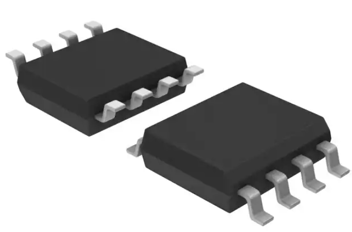


 工商网监
湘ICP备2023018690号
工商网监
湘ICP备2023018690号

