DATA SHEET
Product Name High-Power Thick Film Chip Resistors
Part Name HP Series
File No. SMD-SP-003
Uniroyal Electronics Global Co., Ltd.
88#, Longteng Road, Economic & Technical Development Zone, Kunshan, Jiangsu, China
Tel
Email
Manufacture Plant
+86 512 5763 1411 / 22 /33
marketing@uni-royal.cn
Uniroyal Electronics Industry Co., Ltd.
Aeon Technology Corporation
Royal Electronic Factory (Thailand) Co., Ltd.
Royal Technology (Thailand) Co., Ltd.
�High-Power Thick Film Chip Resistors
1. Scope
1.1 This datasheet is the characteristics of High Power Thick Film Chip Resistors manufactured by UNI-ROYAL.
1.2 High power standard size
1.3 Suitable for both wave & re-flow soldering
1.4 AEC-Q200 qualified
1.5Application:AV adapters,LCD back-light,camera strobe ect.
2. Part No. System
Part No. includes 14 codes shown as below:
2.1 1st~4th codes: Part name. E.g.: HP02、HP03、HP05、HP06、HP07、HP10、HP11、HP12
2.2 5th~6th codes: Power rating.
E.g.: W=Normal Size
“1~G” = “1~16”
Wattage
1/32
3/4
1/2
1/3
1/4
1/8
1/10
1/16
1/20
1
Normal Size
WH
07
W2
W3
W4
W8
WA
WG
WM
1W
If power rating is equal or lower than 1 watt, 5th code would be “W” and 6th code would be a number or letter.
E.g.: WA=1/10W
W4=1/4W
2.3 7th code: Tolerance. E.g.: F=±1%
J=±5%
2.4 8th~11th codes: Resistance Value.
2.4.1 If value belongs to standard value of E-24 series, the 8th code is zero, 9th~10th codes are the significant figures of resistance value, and the
11th code is the power of ten.
2.4.2 If value belongs to standard value of E-96 series, the 8th~10th codes are the significant figures of resistance value, and the 11th code is
the power of ten.
2.4.3 11th codes listed as following:
0=100 1=101
2=102
3=103
4=104
5=105
6=106
J=10-1 K=10-2 L=10-3 M=10-4
th
th
2.5 12 ~14 codes.
2.5.1 12th code: Packaging Type. E.g.: B = Bulk / Box
T=Tape/Reel
2.5.2 13th code: Standard Packing Quantity.
4=4,000pcs
5=5,000pcs
C=10,000pcs
D=20,000pcs
E=15,000pcs
Chip Product: BD=B/B-20000pcs
TC=T/R-10000pcs
2.5.3 14th code: Special features.
E = Environmental Protection, Lead Free, or Standard type.
3. Ordering Procedure
(Example: HP12 2W ±5% 10KΩ T/R-4000)
H
P
1 2
Product Type:
Fill-in 4 digits with
the chip resistor
type as follows:
HP02
HP03
HP05
HP06
HP07
HP10
HP11
HP12
2
W
Wattage:
WA=1/10W
W5=1/5W
W3=1/3W
W2=1/2W
07=3/4W
1W=1W
1Q=1.25W
2W=2W
J
0
1
0
3
T
Resistance Value:
5% (E-24 series):
1st code is zero, 2nd~3rd codes are
the significant figures of
resistance value, and the rest
code is the power of ten.
1% (E-96 series):
1st~3rd codes are the significant
figures of resistance value and
the rest code is the power of ten.
J=10-1; K=10-2; L=10-3
4
E
Packing quantity:
HP02:
C=10000PCS
HP03,HP05,HP06,
HP07:
5=5000PCS
HP10,HP11,HP12:
4=4000PCS
Special Feature
E= Lead-Free
Tolerance:
F=±1% J=±5%
Sep.19,2022 V.2
www. uni-royal.cn
Packing Type:
T=Tape/Reel
Page 2/9
�High-Power Thick Film Chip Resistors
4. Marking
4.1 For HP02 size. Due to the very
small size of the resistor’sbody,
there is no marking on the body.
4.2 Normally, the making of 0Ω HP03, 0Ω HP05,
0Ω HP06,0Ω HP07, 0Ω HP10,0Ω HP11,
0Ω HP12 resistors as following
0 → 0Ω
4.3 ±5% tolerance products (E-24 series):
3 codes.
1st~2nd codes are the significant figures of resistance value,
333 → 33KΩ
and the rest code is the power of ten.
4.4 ±1% tolerance products (E-96 series):
4 codes.
1st~3rd codes are the significant figures of resistance value,
and the rest code is the power of ten.
Letter "R" in mark means decimal point.
4.5 More than HP05 specifications (including) 4 digits,
Product below 1Ω, show as following, the first digit
Is “R” which as decimal point.
2701 → 2.7KΩ
R300 → 0.3Ω
4.6 Standard E-96 series values of 0603 ≤1% : due to the small size of the resistor’s body, 3 digits marking will be used to indicate the accurate
resistance value by using the following multiplier & resistance code.
Multiplier Code (for 0603 ≤±1% marking)
Code
Multiplier
A
10
B
0
10
C
1
10
2
D
10
E
3
10
F
4
10
G
5
10
H
6
10
7
X
-1
10
Y
Z
-2
10-3
10
Standard E-96 series Resistance Value code (for 0603≤±1% marking)
Value
100
Code
01
Value
178
Code
25
Value
316
Code
49
Value
562
Code
73
102
105
02
03
182
187
26
27
324
332
50
51
576
590
74
75
107
110
04
05
191
196
28
29
340
348
52
53
604
619
76
77
113
115
06
07
200
205
30
31
357
365
54
55
634
649
78
79
118
121
08
09
210
215
32
33
374
383
56
57
665
681
80
81
124
127
10
11
221
226
34
35
392
402
58
59
698
715
82
83
130
133
12
13
232
237
36
37
412
422
60
61
732
750
84
85
137
140
14
15
243
249
38
39
432
442
62
63
768
787
86
87
143
147
16
17
255
261
40
41
453
464
64
65
806
825
88
89
150
154
18
19
267
274
42
43
475
487
66
67
845
866
90
91
158
162
20
21
280
287
44
45
499
511
68
69
887
909
92
93
165
169
22
23
294
301
46
47
523
536
70
71
931
953
94
95
174
24
309
48
549
72
976
96
Sep.19,2022 V.2
www. uni-royal.cn
Page 3/9
�High-Power Thick Film Chip Resistors
So the resistance value are marked as the following examples
1.96KΩ=196×101Ω=29B
12.4Ω=124×10-1Ω=10X
4.7 Standard E-24 and not belong to E-96 series values (≤±1%) of 0603 size: the marking is the same as 5% tolerance but marking as underline.
333=33KΩ
680=68Ω
5. Dimension
Type
Dimension(mm)
L
W
H
A
B
HP02(0402)
1.00±0.10
0.50±0.05
0.35±0.05
0.20±0.10
0.25±0.10
HP03(0603)
1.60±0.10
0.80±0.10
0.45±0.10
0.30±0.20
0.30±0.20
HP05(0805)
2.00±0.15
1.25+0.15/ -0.10
0.55±0.10
0.40±0.20
0.40±0.20
HP06(1206)
3.10±0.15
1.55+0.15/-0.10
0.55±0.10
0.45±0.20
0.45±0.20
HP07(1210)
3.10±0.10
2.60±0.20
0.55±0.10
0.50±0.25
0.50±0.20
HP10(2010)
5.00±0.10
2.50±0.20
0.55±0.10
0.60±0.25
0.50±0.20
HP11(1812)
4.50±0.20
3.20±0.20
0.55±0.20
0.50±0.20
0.50±0.20
HP12(2512)
6.35±0.10
3.20±0.20
0.55±0.10
0.60±0.25
0.50±0.20
6. Resistance Range
Type
Size
Power
Rating
HP02
0402
1/10W
HP03
0603
1/5W
HP05
0805
1/3W
HP06
1206
1/2W
HP07
1210
3/4W
HP10
2010
1W
HP11
1812
1.25W
HP12
2512
2W
Sep.19,2022 V.2
Resistance
Range of
1% & 5%
1Ω~10M
0Ω:≤10mΩ
0.1Ω~10M
0Ω:≤8mΩ
0.01Ω~10M
0Ω:≤5mΩ
0.01Ω~10M
0Ω:≤5mΩ
0.1Ω~10M
0Ω:≤4mΩ
0.01Ω~10M
0Ω:≤5mΩ
0.1Ω~10M
0Ω:≤5mΩ
0.01Ω~10M
0Ω:≤5mΩ
Max.
Working
Voltage/Current
50V
3A
75V
5A
150V
6A
200V
10A
200V
12A
200V
12A
200V
12A
300V
16A
www. uni-royal.cn
Max.
Overload
Voltage/ Current
100V
6A
150V
10A
300V
12A
400V
20A
500V
24A
500V
24A
500V
24A
500V
32A
Dielectric
withstanding
Voltage
Operating
Temperature
100V
-55℃~155℃
300V
-55℃~155℃
500V
-55℃~155℃
500V
-55℃~155℃
500V
-55℃~155℃
500V
-55℃~155℃
500V
-55℃~155℃
500V
-55℃~155℃
Page 4/9
�High-Power Thick Film Chip Resistors
7. Soldering pad size recommended
HP02
A
0.5±0.05
Dimension(mm)
B
C
0.5±0.05
0.6±0.05
HP03
HP05
HP06
HP07
HP10
HP11
HP12
0.8±0.05
1.0±0.1
2.0±0.1
2.0±0.1
3.6±0.1
3.0±0.1
4.9±0.1
0.8±0.05
1±0.1
1.1±0.1
1.1±0.1
1.4±0.1
1.4±0.1
1.35±0.1
Type
0.9±0.05
1.4±0.1
1.8±0.1
2.9±0.1
3±0.1
3.7±0.1
3.7±0.1
D
1.5±0.05
2.4±0.05
3±0.1
4.2±0.1
4.2±0.1
6.4±0.1
5.8±0.1
7.6±0.1
8. Derating Curve
Power rating will change based on continuous load at ambient temperature from -55 to 155℃.
It is constant between -55 to 70℃, and derate to zero when temperature rise from 70 to 155℃.
Voltage rating:
Resistors shall have a rated direct-current (DC) continuous working voltage or an approximate sine-wave
root-mean-square (RMS) alternating-current (AC) continuous working voltage at commercial-line
frequency and waveform corresponding to the power rating, as determined from the following formula:
RCWV = √𝑃 × R
Remark: RCWV: Rating Continuous Working Voltage (Volt.) P: power rating (Watt)
R: nominal resistance (Ω)
In no case shall the rated DC or RMS AC continuous working voltage be greater than the applicable maximum value.
The overload voltage is 2.5 times RCWV or Max. Overload voltage whichever is lower.
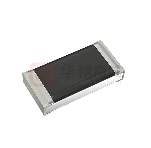
9. Structure
10. Performance Specification
Characteristic
Limits
Ref. Standards
±5%: ±(3.0%+0.1Ω)
±1%: ±(1.0%+0.1Ω)
Operational life
Electrical
Characterization
Sep.19,2022 V.2
Test Methods
125℃, at 36% of operating power, 1000H(1.5 hours
“ON”, 0.5 hour “OFF”).
HP02:


 工商网监
湘ICP备2023018690号
工商网监
湘ICP备2023018690号
