2N3819
Vishay Siliconix
N-Channel JFET
PRODUCT SUMMARY
VGS(off) (V)
v –8
V(BR)GSS Min (V)
–25
gfs Min (mS)
2
IDSS Min (mA)
2
FEATURES
D Excellent High-Frequency Gain: Gps 11 dB @ 400 MHz D Very Low Noise: 3 dB @ 400 MHz D Very Low Distortion D High ac/dc Switch Off-Isolation D High Gain: AV = 60 @ 100 mA
BENEFITS
D D D D D Wideband High Gain Very High System Sensitivity High Quality of Amplification High-Speed Switching Capability High Low-Level Signal Amplification
APPLICATIONS
D D D D High-Frequency Amplifier/Mixer Oscillator Sample-and-Hold Very Low Capacitance Switches
DESCRIPTION
The 2N3819 is a low-cost, all-purpose JFET which offers good performance at mid-to-high frequencies. It features low noise and leakage and guarantees high gain at 100 MHz. Its TO-226AA (TO-92) package is compatible with various tape-and-reel options for automated assembly (see Packaging Information). For similar products in TO-206AF (TO-72) and TO-236 (SOT-23) packages, see the 2N4416/2N4416A/SST4416 data sheet.
TO-226AA (TO-92)
S 1
G
2
D
3
Top View
ABSOLUTE MAXIMUM RATINGS
Gate-Source/Gate-Drain Voltage . . . . . . . . . . . . . . . . . . . . . . . . . . . . . . . –25 V Forward Gate Current . . . . . . . . . . . . . . . . . . . . . . . . . . . . . . . . . . . . . . . . . 10 mA Storage Temperature . . . . . . . . . . . . . . . . . . . . . . . . . . . . . . . . . . . –55 to 150_C Operating Junction Temperature . . . . . . . . . . . . . . . . . . . . . . . . . . –55 to 150_C Document Number: 70238 S–04028—Rev. D ,04-Jun-01 Lead Temperature (1/16” from case for 10 sec.) . . . . . . . . . . . . . . . . . . . 300_C Power Dissipationa . . . . . . . . . . . . . . . . . . . . . . . . . . . . . . . . . . . . . . . . . . . . . . . . . . . 350 mW Notes a. Derate 2.8 mW/_C above 25_C www.vishay.com
7-1
�2N3819
Vishay Siliconix
SPECIFICATIONS (TA = 25_C UNLESS OTHERWISE NOTED)
Limits Parameter Static
Gate-Source Breakdown Voltage Gate-Source Cutoff Voltage Saturation Drain Currentb Gate Reverse Current Gate Operating Currentc Drain Cutoff Current Drain-Source On-Resistance Gate-Source Voltage Gate-Source Forward Voltage V(BR)GSS VGS(off) IDSS IGSS IG ID(off) rDS(on) VGS VGS(F) IG = –1 mA , VDS = 0 V VDS = 15 V, ID = 2 nA VDS = 15 V, VGS = 0 V VGS = –15 V, VDS = 0 V TA = 100_C VDG = 10 V, ID = 1 mA VDS = 10 V, VGS = –8 V VGS = 0 V, ID = 1 mA VDS = 15 V, ID = 200 mA IG = 1 mA , VDS = 0 V –0.5 2 –25 –35 –3 10 –0.002 –0.002 –20 2 150 –2.5 0.7 –7.5 V pA W V –8 20 –2 –2 mA nA mA
Symbol
Test Conditions
Min
Typa
Max
Unit
Dynamic
Common-Source Forward Transconductancec Common-Source Output Conductancec Common-Source Input Capacitance Common-Source Reverse Transfer Capacitance Equivalent Input Noise Voltagec f = 1 kHz gfs gos Ciss Crss en VDS = 15 V VGS = 0 V f = 100 MHz f = 1 kHz VDS = 15 V, VGS = 0 V, f = 1 MHz VDS = 10 V, VGS = 0 V, f = 100 Hz 2 1.6 5.5 5.5 25 2.2 0.7 6 50 8 4 pF nV⁄ √Hz NH 6.5 mS mS
Notes a. Typical values are for DESIGN AID ONLY, not guaranteed nor subject to production testing. b. Pulse test: PW v300 ms, duty cycle v2%. c. This parameter not registered with JEDEC.
TYPICAL CHARACTERISTICS (TA = 25_C UNLESS OTHERWISE NOTED)
Drain Current and Transconductance vs. Gate-Source Cutoff Voltage
20 10 rDS(on) – Drain-Source On-Resistance ( Ω ) gfs – Forward Transconductance (mS) 500 rDS @ ID = 1 mA, VGS = 0 V gos @ VDS = 10 V, VGS = 0 V f = 1 kHz
On-Resistance and Output Conductance vs. Gate-Source Cutoff Voltage
100
IDSS – Saturation Drain Current (mA)
16
IDSS
8
400
80
gos – Output Conductance (mS)
12
gfs
6
300
rDS gos
60
8
4
200
40
4
IDSS @ VDS = 15 V, VGS = 0 V gfs @ VDS = 15 V, VGS = 0 V f = 1 kHz
2
100
20
0 0 –2 –4 –6 –8 –10
0 VGS(off) – Gate-Source Cutoff Voltage (V)
0 0 –2 –4 –6 –8 –10 VGS(off) – Gate-Source Cutoff Voltage (V)
0
www.vishay.com
7-2
Document Number: 70238 S–04028—Rev. D ,04-Jun-01
�2N3819
Vishay Siliconix
TYPICAL CHARACTERISTICS (TA = 25_C UNLESS OTHERWISE NOTED)
100 nA
Gate Leakage Current
10 5 mA
Common-Source Forward Transconductance vs. Drain Current
VGS(off) = –3 V VDS = 10 V f = 1 kHz
10 nA TA = 125_C
gfs – Forward Transconductance (mS)
1 mA 0.1 mA
8 TA = –55_C 6 25_C 4 125_C 2
IG – Gate Leakage
1 nA
100 pA 5 mA 10 pA TA = 25_C 1 mA 0.1 mA
IGSS @ 125_C
1 pA
IGSS @ 25_C
0.1 pA 0 10 VDG – Drain-Gate Voltage (V) 20
0 0.1 1 ID – Drain Current (mA) 10
Output Characteristics
10 VGS(off) = –2 V 8 ID – Drain Current (mA) ID – Drain Current (mA) VGS = 0 V 6 –0.2 V –0.4 V 4 –0.6 V –0.8 V 2 –1.0 V –1.2 V –1.4 V 0 2 4 6 8 10 12 15
Output Characteristics
VGS(off) = –3 V
VGS = 0 V 9 –0.3 V –0.6 V 6 –0.9 V –1.2 V 3 –1.5 V –1.8 V
0
0 0 2 4 6 8 10 VDS – Drain-Source Voltage (V)
VDS – Drain-Source Voltage (V)
Transfer Characteristics
10 VGS(off) = –2 V 8 ID – Drain Current (mA) ID – Drain Current (mA) TA = –55_C 6 25_C VDS = 10 V 8 10
Transfer Characteristics
VGS(off) = –3 V VDS = 10 V
TA = –55_C 6 125_C 4 25_C
4
125_C
2
2
0 0 –0.4 –0.8 –1.2 –1.6 –2 VGS – Gate-Source Voltage (V)
0 0 –0.6 –1.2 –1.8 –2.4 –3 VGS – Gate-Source Voltage (V)
Document Number: 70238 S–04028—Rev. D ,04-Jun-01
www.vishay.com
7-3
�2N3819
Vishay Siliconix
TYPICAL CHARACTERISTICS (TA = 25_C UNLESS OTHERWISE NOTED)
Transconductance vs. Gate-Source Voltage
10 VGS(off) = –2 V gfs – Forward Transconductance (mS) 8 TA = –55_C 6 25_C VDS = 10 V f = 1 kHz gfs – Forward Transconductance (mS) 8 TA = –55_C 6 25_C 10 VGS(off) = –3 V VDS = 10 V f = 1 kHz
Transconductance vs. Gate-Source Voltgage
4
125_C
4
125_C
2
2
0 0 –0.4 –0.8 –1.2 –1.6 –2 VGS – Gate-Source Voltage (V)
0 0 –0.6 –1.2 –1.8 –2.4 –3 VGS – Gate-Source Voltage (V)
On-Resistance vs. Drain Current
300 rDS(on) – Drain-Source On-Resistance ( Ω ) TA = –55_C 240 AV – Voltage Gain VGS(off) = –2 V 180 –3 V 120 80 100
Circuit Voltage Gain vs. Drain Current
g fs R L AV + 1 ) R g L os Assume VDD = 15 V, VDS = 5 V RL + 10 V ID
60
VGS(off) = –2 V 40
60
20 –3 V
0 0.1 1 ID – Drain Current (mA) 10
0 0.1 1 ID – Drain Current (mA) 10
Common-Source Input Capacitance vs. Gate-Source Voltage
5 Crss – Reverse Feedback Capacitance (pF) f = 1 MHz 4 Ciss – Input Capacitance (pF) 3.0
Common-Source Reverse Feedback Capacitance vs. Gate-Source Voltage
f = 1 MHz 2.4
3
VDS = 0 V
1.8
2
1.2
VDS = 0 V
1
VDS = 10 V
0.6
VDS = 10 V
0 0 –4 –8 –12 –16 –20 VGS – Gate-Source Voltage (V)
0 0 –4 –8 –12 –16 –20 VGS – Gate-Source Voltage (V)
www.vishay.com
7-4
Document Number: 70238 S–04028—Rev. D ,04-Jun-01
�2N3819
Vishay Siliconix
TYPICAL CHARACTERISTICS (TA = 25_C UNLESS OTHERWISE NOTED)
Input Admittance
100 TA = 25_C VDS = 15 V VGS = 0 V Common Source 100
Forward Admittance
TA = 25_C VDS = 15 V VGS = 0 V Common Source
bis 10 gis
10 (mS) (mS)
gfs
–bis 1
1
0.1 100
200
500
1000
0.1 100
200
500
1000
f – Frequency (MHz)
f – Frequency (MHz)
Reverse Admittance
10 TA = 25_C VDS = 15 V VGS = 0 V Common Source 10
Output Admittance
TA = 25_C VDS = 15 V VGS = 0 V Common Source
–brs
bos
1 (mS) (mS)
1 gos
–grs 0.1 0.1
0.01 100
200
500
1000
0.01 100
200
500
1000
f – Frequency (MHz)
f – Frequency (MHz)
Equivalent Input Noise Voltage vs. Frequency
20 VGS(off) = –3 V Hz 16 VDS = 10 V gos – Output Conductance (mS) 16 20
Output Conductance vs. Drain Current
VGS(off) = –3 V VDS = 10 V f = 1 kHz
en – Noise Voltage nV /
TA = –55_C 12 25_C 8 125_C 4
12
8 ID = 5 mA 4 ID = IDSS 0 10 100 1k f – Frequency (Hz) 10 k 100 k
0 0.1
1 ID – Drain Current (mA)
10
Document Number: 70238 S–04028—Rev. D ,04-Jun-01
www.vishay.com
7-5
�
很抱歉,暂时无法提供与“2N3819”相匹配的价格&库存,您可以联系我们找货
免费人工找货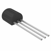


 工商网监
湘ICP备2023018690号
工商网监
湘ICP备2023018690号
