R
UMW
Typ
UMW IRLML6401
P-Channel Enhancement MOSFET
■ Features
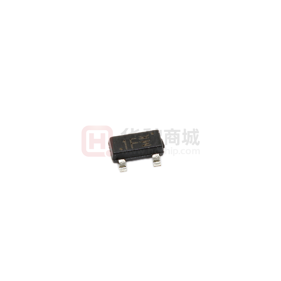
SOT–23
● Ultra low on-resistance.
● P-Channel MOSFET.
● Fast switching.
1. BASE
2. EMITTER
MARKING
3. COLLECTOR
1F MK
■ Absolute Maximum Ratings Ta = 25℃
Parameter
Symbol
Rating
Drain-Source Voltage
VDS
-12
Gate-Source Voltage
VGS
±8
Continuous Drain Current VGS=4.5V @ TA=25℃
Continuous Drain Current
Pulsed Drain Current
VGS=4.5V@ TA=70℃
a
ID
IDM
Power Dissipation
@ TA=25℃
Power Dissipation
@ TA=70℃
PD
Single Pulse Avalanche Energy b
EAS
Thermal Resistance.Junction- to-Ambient
RthJA
Linera Derating Factor
Unit
V
-4.3
-3.4
A
-34
1.3
0.8
W
33
mJ
100
℃/W
0.01
W/℃
Junction Temperature
TJ
150
Junction and Storage Temperature Range
Tstg
-55 to 150
℃
Notes:
a.Repetitive Rating :Pulse width limited by maximum junction temperature
b.Starting TJ=25℃, L=3.5mH, RG=25Ω, IAS=-4.3A
www.umw-ic.com
1
友台半导体有限公司
�R
UMW
Typ
UMW IRLML6401
P-Channel Enhancement MOSFET
■ Electrical Characteristics Ta = 25℃
Parameter
Symbol
Drain-Source Breakdown Voltage
VDSS
Zero Gate Voltage Drain Current
IDSS
Gate-Body leakage current
IGSS
Gate Threshold Voltage
Static Drain-Source On-Resistance
VGS(th)
RDS(On)
Test Conditions
ID=-250μA, VGS=0V
Min
Typ
Max
-12
V
VDS=-12V, VGS=0V
-1
VDS=-9.6V, VGS=0V, TJ= 55℃
-25
-0.4
nA
-0.55 -0.95
V
VGS=-4.5V, ID=-4.3A
50
VGS=-2.5V, ID=-2.5A
85
VGS=-1.8V, ID=-2A
125
VDS=-10V, ID=-4.3A
μA
±100
VDS=0V, VGS=±8V
VDS=VGS ID=-250μA
Unit
8.6
mΩ
S
Forward Transconductance
gFS
Input Capacitance
Ciss
Output Capacitance
Coss
Reverse Transfer Capacitance
Crss
125
Total Gate Charge
Qg
10
15
Gate Source Charge
Qgs
1.4
2.1
Gate Drain Charge
Qgd
2.6
3.9
Turn-On DelayTime
td(on)
11
Turn-On Rise Time
tr
Turn-Off DelayTime
td(off)
Turn-Off Fall Time
tf
Body Diode Reverse Recovery Time
trr
IF=-1.3A, dI/dt=-100A/μs
22
33
Body Diode Reverse Recovery Charge
Qrr
IF=-1.3A, dI/dt=-100A/μs
8
12
Nc
Maximum Body-Diode Continuous Current
IS
1.3
A
-1.2
V
Diode Forward Voltage
www.umw-ic.com
VSD
830
VGS=0V, VDS=-10V, f=1MHz
VGS=-5.0V, VDS=-10V, ID=-4.3A
ID=-1.0A, VDS=-6.0V, RL=6Ω,RGEN=89Ω
pF
180
nC
32
ns
250
210
IS=-1.3A,VGS=0V
2
友台半导体有限公司
�R
UMW
Typ
UMW IRLML6401
P-Channel Enhancement MOSFET
■ Typical Characterisitics
100
VGS
-7.0V
-5.0V
-4.5V
-3.0V
-2.5V
- 1.8V
-1.5V
BOTTOM -1.0V
100
VGS
-7.0V
-5.0V
-4.5V
-3.0V
-2.5V
-1.8V
-1.5V
BOTTOM -1.0V
10
1
-1.0V
0.1
20µs PULSE WIDTH
Tj = 25°C
TOP
-I D, Drain-to-Source Current (A)
-I D, Drain-to-Source Current (A)
TOP
10
1
-1.0V
0.1
20µs PULSE WIDTH
Tj = 150°C
0.01
0.01
0.1
1
10
0.1
100
Fig 1. Typical Output Characteristics
2.0
RDS(on) , Drain-to-Source On Resistance
(Normalized)
-I D , Drain-to-Source Current (Α)
T J = 25°C
T J = 150°C
1.0
VDS = -12V
20µs PULSE WIDTH
1.0
1.5
2.0
2.5
3.0
3.5
4.0
ID = -4.3A
1.5
1.0
0.5
0.0
-60 -40 -20
VGS = -4.5V
0
20
40
60
80 100 120 140 160
TJ , Junction Temperature ( °C)
-V GS, Gate-to-Source Voltage (V)
Fig 3. Typical Transfer Characteristics
www.umw-ic.com
100
Fig 2. Typical Output Characteristics
100.0
0.1
10
-VDS, Drain-to-Source Voltage (V)
-V DS , Drain-to-Source Voltage (V)
10.0
1
Fig 4. Normalized On-Resistance
Vs. Temperature
3
友台半导体有限公司
�R
UMW
Typ
UMW IRLML6401
P-Channel Enhancement MOSFET
■ Typical Characterisitics
1200
Coss = Cds + Cgd
Ciss
800
600
400
Coss
Crss
200
8
6
4
2
0
1
10
ID = -4.3A
VDS =-10V
-VGS , Gate-to-Source Voltage (V)
1000
C, Capacitance(pF)
10
VGS = 0V,
f = 1 MHZ
Ciss = Cgs + Cgd, Cds SHORTED
Crss = Cgd
0
100
0
4
VDS, Drain-to-Source Voltage (V)
16
1000
100
OPERATION IN THIS AREA LIMITED
BY RDS(on)
100
.
-IID , Drain Current (A)
-ISD , Reverse Drain Current (A)
12
Fig 6. Typical Gate Charge Vs.
Gate-to-Source Voltage
Fig 5. Typical Capacitance Vs.
Drain-to-Source Voltage
10
8
QG , Total Gate Charge (nC)
TJ = 150 ° C
TJ = 25 ° C
1
0.6
1.0
1.4
100us
1ms
1
10ms
0.1
0.1
1.8
-VSD ,Source-to-Drain Voltage (V)
Fig 7. Typical Source-Drain Diode
Forward Voltage
www.umw-ic.com
10
TC = 25 ° C
TJ = 150 ° C
Single Pulse
V GS = 0 V
0.1
0.2
10us
1
10
-VDS , Drain-to-Source Voltage (V)
100
Fig 8. Maximum Safe Operating Area
4
友台半导体有限公司
�R
UMW
Typ
UMW IRLML6401
P-Channel Enhancement MOSFET
■ Typical Characterisitics
EAS , Single Pulse Avalanche Energy (mJ)
5.0
-ID , Drain Current (A)
4.0
3.0
2.0
1.0
0.0
25
50
75
100
125
TC , Case Temperature ( ° C)
150
Fig 9. Maximum Drain Current Vs.
Case Temperature
80
ID
-1.9A
-3.4A
BOTTOM -4.3A
TOP
60
40
20
0
25
50
75
100
125
Starting TJ , Junction Temperature ( °C)
150
Fig 10. Maximum Avalanche Energy
Vs. Drain Current
Thermal Response (Z thJA )
1000
100
D = 0.50
0.20
0.10
10
0.05
PDM
0.02
0.01
1
t1
SINGLE PULSE
(THERMAL RESPONSE)
0.1
0.00001
0.0001
t2
Notes:
1. Duty factor D = t 1 / t 2
2. Peak T J = P DM x Z thJA + TA
0.001
0.01
0.1
t1 , Rectangular Pulse Duration (sec)
1
10
Fig 11. Maximum Effective Transient Thermal Impedance, Junction-to-Ambient
www.umw-ic.com
5
友台半导体有限公司
�R
UMW
Typ
UMW IRLML6401
P-Channel Enhancement MOSFET
RDS(on) , Drain-to -Source Voltage ( Ω )
0.10
0.09
0.08
0.07
0.06
0.05
Id = -4.3A
0.04
0.03
0.02
1.0
2.0
3.0
4.0
5.0
6.0
7.0
RDS ( on ) , Drain-to-Source On Resistance ( Ω )
■ Typical Characterisitics
0.20
VGS = -1.8V
VGS = -2.5V
0.15
0.10
VGS = -4.5V
0.05
0.00
0
-VGS, Gate -to -Source Voltage ( V )
10
20
30
40
-I D , Drain Current ( A )
Fig 12. Typical On-Resistance Vs.
Gate Voltage
Fig 13. Typical On-Resistance Vs.
Drain Current
-VGS(th) Gate threshold Voltage (V)
0.8
0.7
ID = -250µA
0.6
0.5
0.4
0.3
-75
-50
-25
0
25
50
75
100
125
150
T J , Temperature ( °C )
Fig 14. Typical Threshold Voltage Vs.
Junction Temperature
www.umw-ic.com
6
友台半导体有限公司
�


 工商网监
湘ICP备2023018690号
工商网监
湘ICP备2023018690号
