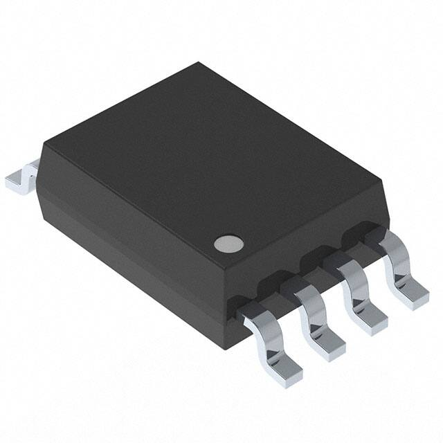
NJM2904C / NJM2904CA
SINGLE-SUPPLY DUAL OPERATIONAL AMPLIFIER
■ GENERAL DESCRIPTION
The NJM2904C / NJM2904CA consists of two independent, high gain,
internally frequency compensated operation amplifiers, which were
designed specifically to operate from a single power supply over a wide
range of voltages. Operation from split power supplies is also possible and
the low power supply current drain is independent of the magnitude of the
power supply voltage.
Application areas include transducer amplifiers, DC gain blocks, and all
the conventional op amp circuits, which now can be more easily
implemented in single power supply systems. For example, the NJM2904C
can be directly operated off of the standard +5V power supply voltage,
which is used in digital systems and will easily provide the required interface
electronics without requiring the additional ±15V power supplies.
■ FEATURES
● Single Supply
● Operating Voltage
● Low Operating Current
● Slew Rate
● Bipolar Technology
● Package Outline
● Internal ESD protection
● Wide temperature range
● Input Offset Voltage Grade
NJM2904CG
NJM2904CAG
(SOP8)
NJM2904CM
NJM2904CAM
(DMP8)
NJM2904CRB1
NJM2904CARB1
(MSOP8(TVSP8))
NJM2904CV
NJM2904CAV
(SSOP8)
NJM2904CME2
(EQFN12-E2)
+3V to +32V
0.7mA typ.
0.6V/μs typ.
SOP8, DMP8 ,SSOP8, EQFN12-E2,
MSOP8 (TVSP8) **MEET JEDEC MO-187-DA / THIN TYPE
Human body model (HBM) ±2000V typ.
-40℃ to +125℃
NJM2904C(Normal-Grade)
7mV max.
NJM2904CA(A-Grade)
2mV max.
■ PIN CONFIGURATION
* NJM2904CME2 don’t have a A version.
(Top
View)
(Top View)
(Top View)
PIN FUNCTION
1.A OUTPUT
2.A - INPUT
A
2
7
3.A + INPUT
4.V
B
3
6
5.B + INPUT
6.B - INPUT
4
5
7.B OUTPUT
+
8.V
NJM2904CG/2904CAG
NJM2904CM/2904CAM
NJM2904CRB1/2904CARB1
NJM2904CV/2904CAV
1
■ PACKAGE OUTLINE
12
11
(Bottom
View)
(Bottom View)
10
10
11
12
8
1
9
9
2
8
8
3
7
7
4
5
6
1
2
PAD
3
6
5
4
PIN FUNCTION
1. A OUTPUT
2. A –INPUT
3. A +INPUT
4. NC
5. V
6. NC
7. B +INPUT
8. B –INPUT
9. B OUTPUT
10. NC
+
11. V
12. NC
NJM2904CME2 (Note1, 2, 3)
(Note1) The PAD have to be wired as short as possible to connect with a V− terminal.
(Note2) The PAD is electronically connected to the backside of the die. But, there cannot be used as V- pin.
(Note3) The NC pin is not internally connected.
■ EQUIVALENT CIRCUIT ( 1/2 Shown )
V+
-INPUT
+INPUT
OUTPUT
V-
Ver.12
-1-
�NJM2904C / NJM2904CA
■ ABSOLUTE MAXIMUM RATINGS
( Ta=25˚C )
PARAMETER
SYMBOL
+
Supply Voltage
RATINGS
-
UNIT
V -V
+32
V
Differential Input Voltage (Note4)
VID
±32
V
Input Voltage
VIN
(Note5)
Output Terminal Input Voltage
Vo
Power Dissipation
PD
Operating Temperature Range
Topr
Storage Temperature Range
Tstg
-
-
V
-
+
V
V - 0.3 to V + 32
SOP
DMP
MSOP
SSOP
EQFN
V - 0.3 to V +0.3
: 690 (Note6) 1000(Note7)
: 470 (Note6) 600 (Note7)
: 510 (Note6) 680 (Note7)
: 430 (Note6) 540(Note7)
: 440 (Note8) 680(Note9)
-40 to +125
mW
˚C
-65 to +150
˚C
(Note4)Differential voltage is the voltage difference between +INPUT and -INPUT.
(Note5) Input voltage is the voltage should be allowed to apply to the input terminal independent of the magnitude of V+.
The normal operation will establish when any input is within the Common Mode Input Voltage Range of electrical characteristics.
(Note6) EIA/JEDEC STANDARD Test board (76.2 x 114.3 x 1.6mm, 2layers, FR-4) mounting
(Note7) EIA/JEDEC STANDARD Test board (76.2 x 114.3 x 1.6mm, 4layers, FR-4) mounting
(Note8) EIA/JEDEC STANDARD Test board (101.5 x 114.3 x 1.6mm, 2layers, FR-4) mounting
(Note9) EIA/JEDEC STANDARD Test board (101.5 x 114.3 x 1.6mm, 4layers, FR-4) mounting
■ELECTRICAL CARACTERISTICS
+
-
(V =5V, V =0V, Ta=25ºC, unless otherwise noted.)
PARAMETER
Supply Current (All amplifiers)
Input Offset Voltage
SYMBOL
ISUPPLY
VIO
TEST CONDITION
MIN.
TYP.
MAX.
+
-
0.7
1.2
V =30V, no signal
+
-
-
2
RS=0Ω
-
0.5
7
RS=0Ω , NJM2904CA
-
0.5
2
V =5V, no signal
UNIT
mA
mV
Input Bias Current
IB
-
20
150
nA
Input Offset Current
IIO
-
2
30
nA
Open-Loop Voltage Gain
Supply Voltage Rejection Ratio
Common Mode Input
Voltage Range
Common Mode Rejection Ratio
Output Source Current
Output Sink Current
AV
RL≥2kΩ
94
100
-
dB
+
65
100
-
dB
V =30V, CMR>70dB
+
0
-
V -1.5
V
Rs
很抱歉,暂时无法提供与“NJM2904CG-TE2”相匹配的价格&库存,您可以联系我们找货
免费人工找货