Freescale Semiconductor
Data Sheet: Technical Data
Document Number: SCF5250EC
Rev. 1.3, 07/2006
SCF5250
Package Information
MAPBGA–196
LQFP-144
SCF5250
Integrated ColdFire®
Microprocessor
Data Sheet
1
Introduction
This document provides an overview of the SCF5250
ColdFire® processor and general descriptions of
SCF5250 features and its various modules.
The SCF5250 was designed as a system
controller/decoder for compressed audio music players,
especially portable and automotive CD and hard disk
drive players. The 32-bit ColdFire core with Enhanced
Multiply Accumulate (EMAC) unit provides optimum
performance and code density for the combination of
control code and signal processing required for audio
decoding and post processing, file management, and
system control.
Ordering Information: See Table 1 on page 2
Contents
1
2
3
4
5
6
Introduction . . . . . . . . . . . . . . . . . . . . . . . . . . 1
SCF5250 Block Diagram . . . . . . . . . . . . . . . . 8
Signal Descriptions . . . . . . . . . . . . . . . . . . . . 8
Electrical Characteristics . . . . . . . . . . . . . . 21
Pin-Out and Package Information . . . . . . . . 36
Product Documentation . . . . . . . . . . . . . . . . 55
Low power features include a hardwired CD ROM
decoder, advanced 0.13um CMOS process technology,
1.2V core power supply, and on-chip 128KByte SRAM
that enables Windows Media Audio (WMA) decoding
without the need for external DRAM in CD applications.
The SCF5250 is also an excellent general purpose
system controller with over 110 Dhrystone 2.1 MIPS @
120MHz performance at a very competitive price. The
This document contains information on a product under development. Freescale reserves the right to change or discontinue this
product without notice.
© Freescale Semiconductor, Inc., 2006. All rights reserved.
�integrated peripherals and enhanced MAC unit allow the SCF5250 to replace both the microcontroller and
the DSP in certain applications. Most peripheral pins can also be remapped as General Purpose I/O pins.
1.1
Orderable Part Numbers
Table 1 lists the orderable part numbers for the SCF5250 processor.
Table 1. Orderable Part Numbers
Orderable Part
Number
Maximum Clock
Frequency
Package Type
Operating Temperature
Range
Part Status
SCF5250LPV100
100 MHz
144 pin QFP
-20°C to 70°C
Leaded
SCF5250LAG100
100 MHz
144 pin QFP
-20°C to 70°C
Lead Free
SCF5250PV120
120 MHz
144 pin QFP
-20°C to 70°C
Leaded
SCF5250AG120
120 MHz
144 pin QFP
-20°C to 70°C
Lead Free
SCF5250DAG1201
120 MHz
144 pin QFP
-20°C to 70°C
Lead Free
SCF5250EAG1202
120 MHz
144 pin QFP
-20°C to 70°C
Lead Free
SCF5250CPV120
120 MHz
144 pin QFP
-40°C to 85°C
Leaded
SCF5250CAG120
120 MHz
144 pin QFP
-40°C to 85°C
Lead Free
SCF5250VM120
120 MHz
196 ball MAPBGA
-20°C to 70°C
Lead Free
1
SCF5250DAG120—This device has the same feature set, pin assignment and specification as SCF5250AG120 with the
addition of including the cost of the MP3 decoder royalty to be paid to Thomson Licensing S.A. for use of the MP3 patent rights
described at http://mp3licensing.com/patents/index.html.
2 SCF5250EAG120—This device has the same feature set, pin assignment and specification as SCF5250AG120 with the
addition of including the cost of the MP3 encoder and decoder royalty to be paid to Thomson Licensing S.A. for use of the MP3
patent rights described at http://mp3licensing.com/patents/index.html.
1.2
SCF5250 Features
This section provides brief descriptions of the features of the SCF5250 processor.
1.2.1
ColdFire V2 Core
The ColdFire processor Version 2 core consists of two independent, decoupled pipeline structures to
maximize performance while minimizing core size.The instruction fetch pipeline (IFP) is a two-stage
pipeline for prefetching instructions. The prefetched instruction stream is then gated into the two-stage
operand execution pipeline (OEP), which decodes the instruction, fetches the required operands, and then
executes the required function. Because the IFP and OEP pipelines are decoupled by an instruction buffer
that serves as a FIFO queue, the IFP can prefetch instructions in advance of their actual use by the OEP,
which minimizes time stalled waiting for instructions. The OEP is implemented in a two-stage pipeline
featuring a traditional RISC data path with a dual-read-ported register file feeding an arithmetic/logic unit
(ALU).
SCF5250 Data Sheet: Technical Data, Rev. 1.3
2
Freescale Semiconductor
�1.2.2
DMA Controller
The SCF5250 provides four fully programmable DMA channels for quick data transfer. Single and dual
address mode is supported with the ability to program bursting and cycle stealing. Data transfer is
selectable as 8, 16, 32, or 128-bits. Packing and unpacking is supported.
Two internal audio channels and the dual UART can be used with the DMA channels. All channels can
perform memory to memory transfers. The DMA controller has a user-selectable, 24- or 16-bit counter and
a programmable DMA exception handler.
External requests are not supported.
1.2.3
Enhanced Multiply and Accumulate Module (EMAC)
The integrated EMAC unit provides a common set of DSP operations and enhances the integer multiply
instructions in the ColdFire architecture. The EMAC provides functionality in three related areas:
1. Faster signed and unsigned integer multiplies
2. New multiply-accumulate operations supporting signed and unsigned operands
3. New miscellaneous register operations
Multiplies of 16x16 and 32x32 with 48-bit accumulates are supported in addition to a full set of extensions
for signed and unsigned integers plus signed, fixed-point fractional input operands. The EMAC has a
single-clock issue for 32x32-bit multiplication instructions and implements a four-stage execution
pipeline.
1.2.4
Instruction Cache
The instruction cache improves system performance by providing cached instructions to the execution unit
in a single clock. The SCF5250 processor uses a 8K-byte, direct-mapped instruction cache to achieve 107
MIPS at 120 MHz. The cache is accessed by physical addresses, where each 16-byte line consists of an
address tag and a valid bit. The instruction cache also includes a bursting interface for 16-bit and 8-bit port
sizes to quickly fill cache lines.
1.2.5
Internal 128-KByte SRAM
The 128-KByte on-chip SRAM is available in two banks, SRAM0 (64K) and SRAM1 (64K). It provides
one clock-cycle access for the ColdFire core. This SRAM can store processor stack and critical code or
data segments to maximize performance. Memory in SRAM1 can be accessed under DMA.
1.2.6
SDRAM Controller
The SCF5250 SDRAM controller provides a glueless interface for one bank of SDRAM up to 32 MB
(256 Mbits). The controller supports a 16-bit data bus. A unique addressing scheme allows for increases
in system memory size without rerouting address lines and rewiring boards. The controller operates in
page mode, non-page mode, and burst-page mode and supports SDRAMS.
SCF5250 Data Sheet: Technical Data, Rev. 1.3
Freescale Semiconductor
3
�1.2.7
System Interface
The SCF5250 provides a glueless interface to 16-bit port size SRAM, ROM, and peripheral devices with
independent programmable control of the assertion and negation of chip-select and write-enable signals.
The SCF5250 also supports bursting ROMs.
1.2.8
External Bus Interface
The bus interface controller transfers information between the ColdFire core or DMA and memory,
peripherals, or other devices on the external bus. The external bus interface provides 23 bits of address bus
space, a 16-bit data bus, Output Enable, and Read/Write signals. This interface implements an extended
synchronous protocol that supports bursting operations.
1.2.9
Serial Audio Interfaces
The SC5250 digital audio interface provides three serial Philips IIS/Sony EIAJ interfaces. One interface
is a 4-pin (1 bit clock, 1 word clock, 1 data in, 1 data out), the other two interfaces are 3-pin (1 bit clock,
1 word clock, 1 data in or out). The serial interfaces have no limit on minimum sampling frequency.
Maximum sampling frequency is determined by maximum frequency on bit clock input. This is 1/3 the
frequency of the internal system clock.
1.2.10
IEC958 Digital Audio Interfaces
The SCF5250 has one digital audio input interface, and one digital audio output interface. The single
output carries the consumer “c” channel.
1.2.11
Audio Bus
The audio interfaces connect to an internal bus that carries all audio data. Each receiver places its received
data on the audio bus and each transmitter takes data from the audio bus for transmission. Each transmitter
has a source select register.
In addition to the audio interfaces, there are six CPU accessible registers connected to the audio bus. Three
of these registers allow data reads from the audio bus and allow selection of the audio source. The other
three register provide a write path to the audio bus and can be selected by transmitters as the audio source.
Through these registers, the CPU has access to the audio samples for processing.
Audio can be routed from a receiver to a transmitter without the data being processed by the core so the
audio bus can be used as a digital audio data switch. The audio bus can also be used for audio format
conversion.
1.2.12
CD-ROM Encoder/Decoder
The SCF5250 is capable of processing CD-ROM sectors in hardware. Processing is compliant with
CD-ROM and CD-ROM XA standards.
SCF5250 Data Sheet: Technical Data, Rev. 1.3
4
Freescale Semiconductor
�The CD-ROM decoder performs following functions in hardware:
• Sector sync recognition
• Descrambling of sectors
• Verification of the CRC checksum for Mode 1, Mode 2 Form 1, and Mode 2 Form 2 sectors
• Third-layer error correction is not performed
The CD-ROM encoder performs following functions in hardware:
• Sector sync recognition
• Scrambling of sectors
• Insertion of the CRC checksum for Mode 1, Mode 2 Form 1, and Mode 2 Form 2 sectors.
• Third-layer error encoding needs to be done in software. This can use approximately 5–10 MHz of
performance for single-speed.
1.2.13
Dual UART Module
Two full-duplex UARTs with independent receive and transmit buffers are in this module. Data formats
can be 5, 6, 7, or 8 bits with even, odd, or no parity, and up to 2 stop bits in 1/16 increments. Four-byte
receive buffers and two-byte transmit buffers minimize CPU service calls. The Dual UART module also
provides several error-detection and maskable-interrupt capabilities. Modem support includes
request-to-send (RTS) and clear-to-send (CTS) lines.
The system clock provides the clocking function from a programmable prescaler. You can select full
duplex, auto-echo loopback, local loopback, and remote loopback modes. The programmable Dual UARTs
can interrupt the CPU on various normal or error-condition events.
1.2.14
Queued Serial Peripheral Interface QSPI
The QSPI module provides a serial peripheral interface with queued transfer capability. It supports up to
16 stacked transfers at a time, making CPU intervention between transfers unnecessary. Transfers of up to
15 Mbits/second are possible at a CPU clock of 120 MHz. The QSPI supports master mode operation only.
1.2.15
Timer Module
The timer module includes two general-purpose timers, each of which contains a free-running 16-bit timer.
Timer0 has an external pin TOUT0, which can be used in Output Compare mode. This mode triggers an
external signal or interrupts the CPU when the timer reaches a set value, and can also generate waveforms
on TOUT0.
The timer unit has an 8-bit prescaler that allows programming of the clock input frequency, which is
derived from the system clock. In addition to the ÷1 and ÷16 clock derived from the bus clock (CPU clock
/ 2), the programmable timer-output pins either generate an active-low pulse or toggle the outputs.
SCF5250 Data Sheet: Technical Data, Rev. 1.3
Freescale Semiconductor
5
�1.2.16
IDE and SmartMedia Interfaces
The SCF5250 system bus allows connection of an IDE hard disk drive or SmartMedia flash card with a
minimum of external hardware. The external hardware consists of bus buffers for address and data and are
intended to reduce the load on the bus and prevent SDRAM and Flash accesses to propagate to the IDE
bus. The control signals for the buffers are generated in the SCF5250.
Low cost version SCF5250LPV100 and SCF5250LAG100 does not run production test for the
IDE/CF/SD/MMC interfaces. Freescale does not guarantee these interfaces will work on these two
devices.
1.2.17
Analog/Digital Converter (ADC)
The six channel ADC is a based on the Sigma-Delta concept with 12-bit resolution. Both the analogue
comparator and digital sections of the ADC are provided internally. An external integrator circuit
(resistor/capacitor) is required, which is driven by the ADC output. A software interrupt is provided when
the ADC measurement cycle is complete.
1.2.18
I2C Module
The two-wire I2C bus interface, which is compliant with the Philips I2C bus standard, is a bidirectional
serial bus that exchanges data between devices. The I2C bus minimizes the interconnection between
devices in the end system and is best suited for applications that need occasional bursts of rapid
communication over short distances among several devices. Bus capacitance and the number of unique
addresses limit the maximum communication length and the number of devices that can be connected.
1.2.19
Chip-Selects
Up to four programmable chip-select outputs provide signals that enable glueless connection to external
memory and peripheral circuits. The base address, access permissions and automatic wait-state insertion
are programmable with configuration registers. These signals also interface to 16-bit ports.
CS0 is active after reset to provide boot-up from external FLASH/ROM.
1.2.20
GPIO Interface
A total of 60 General Purpose inputs and 57 General Purpose outputs are available. These are multiplexed
with various other signals. Seven of the GPIO inputs have edge sensitive interrupt capability.
1.2.21
Interrupt Controller
The interrupt controller provides user-programmable control of a total of 57 interrupts. There are 49
internal interrupt sources. In addition, there are 7 GPIOs where interrupts can be generated on the rising
or falling edge of the pin. All interrupts are autovectored and interrupt levels are programmable.
SCF5250 Data Sheet: Technical Data, Rev. 1.3
6
Freescale Semiconductor
�1.2.22
JTAG
To help with system diagnostics and manufacturing testing, the SCF5250 includes dedicated
user-accessible test logic that complies with the IEEE 1149.1A standard for boundary scan testability,
often referred to as Joint Test Action Group, or JTAG. For more information, refer to the IEEE 1149.1A
standard. Freescale provides BSDL files for JTAG testing.
1.2.23
System Debug Interface
The ColdFire processor core debug interface supports real-time instruction trace and debug, plus
background-debug mode. A background-debug mode (BDM) interface provides system debug.
In real-time instruction trace, four status lines provide information on processor activity in real time (PST
pins). A four-bit wide debug data bus (DDATA) displays operand data and change-of-flow addresses,
which helps track the machine’s dynamic execution path.
1.2.24
Crystal and On-Chip PLL
Typically, an external 16.92 MHz or 33.86 MHz clock input is used for CD R/W applications, while an
11.2896 MHz clock is more practical for Portable CD player applications. However, the on-chip
programmable PLL, which generates the processor clock, allows the use of almost any low frequency
external clock (5-35 MHz).
Two clock outputs (MCLK1 and MCLK2) are provided for use as Audio Master Clock. The output
frequencies of both outputs are programmable to Fxtal, Fxtal/2, Fxtal/3, and Fxtal/4. The Fxtal/3 option is
only available when the 33.86 MHz crystal is connected.
The SCF5250 supports VCO operation of the oscillator by means of a 16-bit pulse density modulation
output. Using this mode, it is possible to lock the oscillator to the frequency of an incoming IEC958 or IIS
signal. The maximum trim depends on the type and design of the oscillator. Typically a trim of +/- 100 ppm
can be achieved with a crystal oscillator and over +/- 1000 ppm with an LC oscillator.
1.2.25
Boot ROM
The boot ROM on the SCF5250 serves to boot the CPU in designs which do not have external Flash
memory or ROM. Typically this occurs in systems which have a separate MCU to control the system,
and/or the SCF5250 is used as a stand-alone decoder.
The SCF5250 can be booted in one of three modes:
• External ROM
• Internal ROM Master mode – boots from I2C, SPI, or IDE
• Internal ROM Slave mode – boots from I2C or UART
1.2.26
Voltage Regulator
The SCF5250 contains an on-chip linear regulator that generates 1.2V from a 3.3V input. The regulator is
self-contained and drives the 1.2V core voltage out on one pin that can be used to power the core supply
SCF5250 Data Sheet: Technical Data, Rev. 1.3
Freescale Semiconductor
7
�pins at the board level. In battery powered portable applications, it is recommended that an external dc-dc
converter be used to generate the 1.2V core voltage to minimize power consumption.
2
SCF5250 Block Diagram
Figure 1 illustrates the functional block diagram of the SCF5250 processor.
Flash
Media Int
CD ROM
block encode
& decode
I2S Rx
x3
I2S Tx
x2
IDE
Interface
12-bit
ADC
UART x2
SPDIF
Tx
QSPI
I2C x2
DMAs /
Timers
SPDIF
Rx
BDM
PLL
GPI/O
1.2V
Regulator
JTAG
Boot
ROM
128K
SRAM
8K
Oscillator
EMAC
I-Cache
V2
ColdFire®
Core
System
Bus
Controller
SDRAM Ctr
&
Chip Selects
Figure 1. SCF5250 Block Diagram
3
Signal Descriptions
This section describes the SCF5250 processor’s input and output signals. The signal descriptions shown
in Table 2 are grouped according to relevant functionality.
SCF5250 Data Sheet: Technical Data, Rev. 1.3
8
Freescale Semiconductor
�Table 2. SCF5250 Signal Index
Signal Name
Mnemonic
Function
Input/ Reset
Output State
Address
A[24:1]
A[23]/GPO54
24 address lines, address line 23
multiplexed with GPO54 and address 24
is multiplexed with A20 (SDRAM access
only).
Out
X
Read-write control
R/W
Bus write enable - indicates if read or
write cycle in progress
Out
H
Output enable
OE
Output enable for asynchronous
memories connected to chip selects
Out
negated
Data
D[31:16]
Data bus used to transfer word data
In/Out
Hi-Z
Synchronous row address SDRAS/GPIO59
strobe
Row address strobe for external SDRAM.
Out
negated
Synchronous column
address strobe
SDCAS/GPIO39
Column address strobe for external
SDRAM
Out
negated
SDRAM write enable
SDWE/GPIO38
Write enable for external SDRAM
Out
negated
SDRAM upper byte
enable
SDUDQM/GPO53
Indicates during write cycle if high byte is
written
Out
–
SDRAM lower byte enable SDLDQM/GPO52
Indicates during write cycle if low byte is
written
Out
–
SDRAM chip selects
SD_CS0/GPIO60
SDRAM chip select
SDRAM clock enable
BCLKE/GPIO63
SDRAM clock enable
Out
–
System clock
BCLK/GPIO40
SDRAM clock output
In/Out
–
ISA bus read strobe
IDE-DIOR/GPIO31
(CS2)
–
ISA bus write strobe
IDE-DIOW/GPIO32
(CS2)
There is 1 ISA bus read strobe and 1 ISA In/Out
bus write strobe. They allow connection
of one independent ISA bus peripherals,
In/Out
e.g. an IDE slave device.
ISA bus wait signal
IDE-IORDY/GPIO33
ISA bus wait line - available for both
busses
In/Out
Chip Selects[2:0]
CS0/CS4
CS1/QSPI_CS3/GPIO28
Enables peripherals at programmed
addresses.
CS[0] provides boot ROM selection
Out negated
In/Out
Buffer enable 1
BUFENB1/GPIO29
In/Out
–
Buffer enable 2
BUFENB2/GPIO30
Two programmable buffer enables allow
seamless steering of external buffers to
split data and address bus in sections.
In/Out
–
Transfer acknowledge
TA/GPIO12
Transfer Acknowledge signal
In/Out
–
Wake Up
WAKE_UP/GPIO21
Wake-up signal input
In
–
In/Out negated
2
–
–
Serial Clock Line
SCL0/SDATA1_BS1/GPIO41
SCL1/TXD1/GPIO10
Clock signal for Dual I C module
operation
In/Out
–
Serial Data Line
SDA0/SDATA3/GPIO42
SDA1/RXD1/GPIO44
Serial data port for second I2C module
operation
In/Out
–
Receive Data
SDA1/RXD1/GPIO44
RXD0/GPIO46
Signal is receive serial data input for
DUART
In
–
SCF5250 Data Sheet: Technical Data, Rev. 1.3
Freescale Semiconductor
9
�Table 2. SCF5250 Signal Index (continued)
Signal Name
Mnemonic
Input/ Reset
Output State
Function
Transmit Data
SCL1/TXD1/GPIO10
TXD0/GPIO45
Signal is transmit serial data output for
DUART
Out
–
Request-To-Send
DDATA3/RTS0/GPIO4
DDATA1/RTS1/SDATA2_BS2/GPIO2
DUART signals a ready to receive data
query
Out
–
Clear-To-Send
DDATA2/CTSO/GPIO3
Signals to DUART that data can be
DDATA0/CTS1/SDATA0_SDIO1/GPIO1 transmitted to peripheral
In
–
Timer Output
SDATAO1/TOUT0/GPIO18
Capable of output waveform or pulse
generation
Out
–
IEC958 inputs
EBUIN1/GPIO36
EBUIN2/SCLK_OUT/GPIO13
EBUIN3/CMD_SDIO2/GPIO14
QSPI_CS0/EBUIN4/GPIO15
audio interfaces IEC958 inputs
In
–
IEC958 outputs
EBUOUT1/GPIO37
QSPI_CS1/EBUOUT2/GPIO16
audio interfaces IEC958 outputs
Out
–
Serial data in
SDATAI1/GPIO17
SDATAI3/GPIO8
audio interfaces serial data inputs
In
–
Serial data out
SDATAO1/TOUT0/GPIO18
SDATAO2/GPIO34
audio interfaces serial data outputs
In/Out
Out
–
Word clock
LRCK1/GPIO19
LRCK2/GPIO23
LRCK3/GPIO43/AUDIO_CLOCK
audio interfaces serial word clocks
In/Out
–
Bit clock
SCLK1/GPIO20
SCLK2/GPIO22
SCLK3/GPIO35
audio interfaces serial bit clocks
In/Out
–
Serial input
EF/GPIO6
error flag serial in
In/Out
–
Serial input
CFLG/GPIO5
C-flag serial in
In/Out
–
Subcode clock
RCK/QSPI_DIN/QSPI_DOUT/
GPIO26
audio interfaces subcode clock
In/Out
–
Subcode sync
QSPI_DOUT/SFSY/GPIO27
audio interfaces subcode sync
In/Out
–
Subcode data
QSPI_CLK/SUBR/GPIO25
audio interfaces subcode data
In/Out
–
Clock frequency trim
XTRIM/GPIO0
clock trim control
Out
–
Audio clocks out
MCLK1/GPIO11
QSPI_CS2/MCLK2/GPIO24
DAC output clocks
Out
–
Audio clock in
LRCK3/GPIO43/AUDIO_CLOCK
Optional Audio clock Input
–
–
SCF5250 Data Sheet: Technical Data, Rev. 1.3
10
Freescale Semiconductor
�Table 2. SCF5250 Signal Index (continued)
Signal Name
Memory Stick/
Secure Digital interface
Mnemonic
Function
Input/ Reset
Output State
EBUIN3/CMD_SDIO2/GPIO14
Secure Digital command lane
Memory Stick interface 2 data I/O
In/Out
–
EBUIN2/SCLK_OUT/GPIO13
Clock out for both Memory Stick
interfaces and for Secure Digital
In/Out
–
DDATA0/CTS1/SDATA0_SDIO1/GPIO1 Secure Digital serial data bit 0
Memory Stick interface 1 data I/O
In/Out
–
SCL0/SDATA1_BS1/GPIO41
Secure Digital serial data bit 1
Memory Stick interface 1 strobe
In/Out
–
DDATA1/RTS1/SDATA2_BS2/GPIO2
Secure Digital serial data bit 2
Memory Stick interface 2 strobe
Reset output signal
In/Out
–
SDA0/SDATA3/GPIO42
Secure Digital serial data bit 3
In/Out
–
ADC IN
ADIN0/GPI52
ADIN1/GPI53
ADIN2/GPI54
ADIN3/GPI55
ADIN4/GPI56
ADIN5/GPI57
Analog to Digital converter input signals
In
–
ADC OUT
ADREF
ADOUT/SCLK4/GPIO58
Analog to digital convertor output signal.
Connect to ADREF via integrator
network.
In/Out
–
QSPI clock
QSPI_CLK/SUBR/GPIO25
QSPI clock signal
In/Out
–
QSPI data in
RCK/QSPI_DIN/QSPI_DOUT/GPIO26
QSPI data input
In/Out
–
QSPI data out
RCK/QSPI_DIN/QSPI_DOUT/GPIO26
QSPI_DOUT/SFSY/GPIO27
QSPI data out
In/Out
–
QSPI chip selects
QSPI_CS0/EBUIN4/GPIO15
QSPI_CS1/EBUOUT2/GPIO16
QSPI_CS2/MCLK2/GPIO24
CS1/QSPI_CS3/GPIO28
QSPI chip selects
In/Out
–
Crystal in
CRIN
Crystal input
In
–
Crystal out
CROUT
Crystal Out
Out
–
Reset In
RSTI
Processor Reset Input
In
–
Freescale Test Mode
TEST[2:0]
TEST pins.
In
–
Linear regulator output
LINOUT
outputs 1.2 V to supply core
Out
–
Linear regulator input
LININ
Input, typically I/O supply (3.3V)
In
–
Linear regulator ground
LINGND
–
–
–
High Impedance
HI-Z
Assertion Tri-states all output signal pins.
In
–
Debug Data
DDATA0/CTS1/SDATA0_SDIO1/GPIO1 Displays captured processor data and
break-point status.
DDATA1/RTS1/SDATA2_BS2/GPIO2
DDATA2/CTS0/GPIO3
DDATA3/RTS0/GPIO4
In/Out
Hi-Z
SCF5250 Data Sheet: Technical Data, Rev. 1.3
Freescale Semiconductor
11
�Table 2. SCF5250 Signal Index (continued)
Signal Name
Mnemonic
Input/ Reset
Output State
Function
Processor Status
PST0/GPIO50
PST1/GPIO49
PST2/INTMON2/GPIO48
PST3/INTMON1/GPIO47
Indicates internal processor status.
In/Out
Hi-Z
Processor Clock
PSTCLK/GPIO51
processor clock output
Out
–
Test Clock
TCK
Clock signal for IEEE 1149.1A JTAG.
In
–
Test Reset/Development
Serial Clock
TRST/DSCLK
Multiplexed signal that is asynchronous
reset for JTAG controller. Clock input for
debug module.
In
–
Test Mode Select/ Break
Point
TMS/BKPT
Multiplexed signal that is test mode select
in JTAG mode and a hardware
break-point in debug mode.
In
–
Test Data Input /
TDI/DSI
Development Serial Input
Multiplexed serial input for the JTAG or
background debug module.
In
–
Test Data
Output/Development
Serial Output
Multiplexed serial output for the JTAG or
background debug module.
Out
–
3.1
TDO/DSO
GPIO
Many pins have an optional GPIO function.
• General purpose input is always active, regardless of state of pin.
• General purpose output or primary output is determined by the appropriate setting of the Pin
Multiplex Control Registers, GPIO-FUNCTION, GPIO1-FUNCTION and PIN-CONFIG.
• At Power-on reset, all pins are set to their primary function.
3.2
SCF5250 Bus Signals
These signals provide the external bus interface to the SCF5250 processor.
3.2.1
•
•
Address Bus
The address bus provides the address of the byte or most significant byte of the word or longword
being transferred. The address lines also serve as the DRAM address pins, providing multiplexed
row and column address signals.
Bits 23 down to 1 and 24 of the address are available. A24 is intended to be used with 256 Mbit
DRAM’s. Signals are named:
— A[23:1]
— A20/24
SCF5250 Data Sheet: Technical Data, Rev. 1.3
12
Freescale Semiconductor
�3.2.2
Read-Write Control
This signal indicates during any bus cycle whether a read or write is in progress. A low is write cycle and
a high is a read cycle.
3.2.3
Output Enable
The OE signal is intended to be connected to the output enable of asynchronous memories connected to
chip selects. During bus read cycles, the ColdFire processor will drive OE low.
3.2.4
Data Bus
The data bus (D[31:16]) is bi-directional and non-multiplexed. Data is registered by the SCF5250 on the
rising clock edge. The data bus uses a default configuration if none of the chip-selects or DRAM bank
match the address decode. All 16 bits of the data bus are driven during writes, regardless of port width or
operand size.
3.2.5
Transfer Acknowledge
The TA/GPIO12 pin is the transfer acknowledge signal.
3.3
SDRAM Controller Signals
The following SDRAM signals provide a glueless interface to external SDRAM. An SDRAM width of 16
bits is supported and can access as much as 32MB of memory. ADRAMs are not supported.
Table 3. SDRAM Controller Signals
SDRAM Signal
Description
Synchronous DRAM row address strobe
The SDRAS/GPIO59 active low pin provides a seamless interface to the RAS input
on synchronous DRAM
Synchronous DRAM Column Address
Strobe
The SDCAS/GPIO39 active low pin provides a seamless interface to CAS input on
synchronous DRAM.
Synchronous DRAM Write
The SDWE/GPIO38 active-low pin is asserted to signify that a SDRAM write cycle
is underway. This pin outputs logic ‘1’ during read bus cycles.
Synchronous DRAM Chip Enable
The SD_CS0/GPIO60 active-low output signal is used during synchronous mode
to route directly to the chip select of a SDRAM device.
Synchronous DRAM UDQM and LQDM
signals
The DRAM byte enables UDMQ and LDQM are driven by the SDUDQM/GPO53
and SDLDQM/GPO52 byte enable outputs.
Synchronous DRAM clock
The DRAM clock is driven by the BCLK/GPIO40 signal
Synchronous DRAM Clock Enable
The BCLKE active high output signal is used during synchronous mode to route
directly to the SCKE signal of external SDRAMs. This signal provides the clock
enable to the SDRAM.
SCF5250 Data Sheet: Technical Data, Rev. 1.3
Freescale Semiconductor
13
�3.4
Chip Selects
There are three chip select outputs on the SCF5250 device. CS0/CS4 and CS1/QSPI_CS3/GPIO28 and
CS2 which is associated with the IDE interface read and write strobes - IDE-DIOR and IDE-DIOW.
CS0 and CS4 are multiplexed. The SCF5250 has the option to boot from an internal Boot ROM.
The function of the CS0/CS4 pin is determined by the boot mode. When the device is booted from internal
ROM, the internal ROM is accessed with CS0 (required for boot) and the CS0/CS4 pin is driven by CS4.
When the device is booted from external ROM / Flash, the CS0/CS4 pin is driven by CS0 and the internal
ROM is disabled.
The active low chip selects can be used to access asynchronous memories. The interface is glueless.
3.5
ISA Bus
The SCF5250 supports an ISA bus. Using the ISA bus protocol, reads and writes for one ISA bus
peripheral is possible. IDE-DIOR/GPIO31 and IDE-DIOW/GPIO32 are the read and write strobe. The
peripheral can insert wait states by pulling IDE-IORDY/GPIO33.
CS2 is associated with the IDE-DIOR and IDE-DIOW.
3.6
Bus Buffer Signals
As the SCF5250 has a complicated slave bus, which allows SDRAM, asynchronous memories, and ISA
peripherals on the bus, it may become necessary to introduce a buffer on the bus in certain applications.
The SCF5250 has a glueless interface to steer these bus buffers with two bus buffer output signals
BUFENB1/GPIO29 and BUFENB2/GPIO30.
3.7
I2C Module Signals
There are two I2C interfaces on this device as described in Table 4.
The I2C module acts as a two-wire, bidirectional serial interface between the SCF5250 processor and
peripherals with an I2C interface (e.g., LED controller, A-to-D converter, D-to-A converter). When
devices connected to the I2C bus drive the bus, they will either drive logic-0 or high-impedance. This can
be accomplished with an open-drain output.
Table 4. I2C Module Signals
I2c Module Signal
Description
I2C Serial Clock
The SCL0/SDATA1_BS1/GPIO41 and SCL1/TXD1/GPIO10 bidirectional signals are the clock signal for
first and second I2C module operation. The I2C module controls this signal when the bus is in master
mode; all I2C devices drive this signal to synchronize I2C timing.
Signals are multiplexed
I2C Serial Data
The SDA0/SDATA3/GPIO42 and SDA1/RXD1/GPIO44 bidirectional signals are the data input/output for
the first and second serial I2C interface.
Signals are multiplexed
SCF5250 Data Sheet: Technical Data, Rev. 1.3
14
Freescale Semiconductor
�3.8
Serial Module Signals
The signals described in Table 5 transfer serial data between the two UART modules and the external
peripherals.
Table 5. Serial Module Signals
Serial Module Signal
Description
Receive Data
The RXD0/GPIO46 and SDA1/RXD1/GPIO44 are the inputs on which serial data is received by the
DUART. Data is sampled on RxD[1:0] on the rising edge of the serial clock source, with the least
significant bit received first.
Transmit Data
The DUART transmits serial data on the TXD0/GPIO45 and SCL1/TXD1/GPIO10 output signals. Data
is transmitted on the falling edge of the serial clock source, with the least significant bit transmitted (LSB)
first. When no data is being transmitted or the transmitter is disabled, these two signals are held high.
TxD[1:0] are also held high in local loopback mode.
Request To Send
The DDATA3/RTS0/GP104 and DDATA1/RTS1/SDATA2_BS2/GPIO2 request-to-send outputs indicate
to the peripheral device that the DUART is ready to send data and requires a clear-to-send signal to
initiate transfer.
Clear To Send
3.9
Peripherals drive the DDATA2/CTS0/GPIO3 and DDATA0/CTS1/SDATA0_SDIO1/GPIO1 inputs to
indicate to the SCF5250 serial module that it can begin data transmission.
Timer Module Signals
Table 6 describes the Timer module signal which provides an external interface to Timer0.
Table 6. Timer Module Signals
Serial Module Signal
Timer Output
Description
The SDATAO1/TOUT0/GPIO18 programmable output pulse or toggle on various timer events.
SCF5250 Data Sheet: Technical Data, Rev. 1.3
Freescale Semiconductor
15
�3.10
Serial Audio Interface Signals
Table 7 describes the signals that provide the external audio interface.
Table 7. Serial Audio Interface Signals
Serial Module Signal
Description
Serial Audio Bit Clock
The SCLK1/GPIO20, SCLK2/GPIO22 and SCLK3/GPIO35,
multiplexed pins can serve as general purpose I/Os or serial audio bit clocks. As bit clocks, these
bidirectional pins can be programmed as outputs to drive their associated serial audio (IIS) bit clocks.
Alternately, these pins can be programmed as inputs when the serial audio bit clocks are driven
internally. The functionality is programmed within the Audio module. During reset, these pins are
configured as input serial audio bit clocks.
Serial Audio Word Clock The LRCK1/GPIO19, LRCK2/GPIO23 and LRCK3/GPIO43/AUDIO_CLOCK multiplexed pins can
serve as general purpose I/Os or serial audio word clocks. As word clocks, the bidirectional pins can
be programmed as inputs to drive their associated serial audio word clock. Alternately, these pins can
be programmed as outputs when the serial audio word clocks are derived internally. The functionality
is programmed within the Audio module. During reset, these pins are configured as input serial audio
word clocks.
LRCK3/GPIO43/AUDIO_CLOCK can be used as the external audio clock input. If the core clock
chosen to be non-audio specific.
Serial Audio Data In
The SDATAI1/GPIO17 and SDATAI3/GPIO8 multiplexed pins can serve as general purpose I/Os or
serial audio inputs. As serial audio inputs the data is sent to interfaces 1and 3 respectively. During
reset, the pins are configured as serial data inputs.
Serial Audio Data Out
SDATO1/TOUT0/GPIO18 AND SDATAO2/GPIO34 multiplexed pins can serve as general purpose I/Os
or serial audio outputs. During reset, the pins are configured as serial data outputs.
Serial audio error flag
The EF/GPIO6 multiplexed pin can serve as general purpose I/Os or error flag input. As error flag
input, this pin will input the error flag delivered by the CD-DSP. EF/GPIO6 is only relevant for serial
interface SDATAI1.
Serial audio CFLG
The CFLG/GPIO5 multiplexed pin can serve as general purpose I/O or CFLG input. As CFLG input,
the pin will input the CFLG flag delivered by the CD-DSP. CFLG/GPIO5 is only relevant for serial
interface SDATAI1.
3.11
Digital Audio Interface Signals
Table 8 describes the signals for the digital audio interface.
Table 8. Digital Audio Interface Signals
Serial Module Signal
Description
Digital Audio In
The EBUIN1/GPIO36, EBUIN2/SCLK_OUT/GPIO13, EBUIN3/CMD_SDIO2/GPIO14, and
QSPI_CS0/EBUIN4/GPIO15 multiplexed signals can serve as general purpose input or can be driven
by various digital audio (IEC958) input sources. Both functions are always active. Input chosen for
IEC958 receiver is programmed within the audio module. Input value on the 4 pins can always be read
from the appropriate GPIO register.
Digital Audio Out
The EBUOUT1/GPIO37 and QSPI_CS1/EBUOUT2/GPIO16 multiplexed pins can serve as general
purpose I/O or as digital audio (IEC958) output. EBUOUT1 is digital audio out for consumer mode,
EBUOUT2 is digital audio out for professional mode. During reset, the pin is configured as a digital audio
output.
SCF5250 Data Sheet: Technical Data, Rev. 1.3
16
Freescale Semiconductor
�3.12
Subcode Interface
There is a 3-line subcode interface on the SCF5250 processor. This 3-line subcode interface allows the
device to format and transmit subcode in EIAJ format to a CD channel encoder device. The three signals
are described in Table 9.
Table 9. Subcode Interface Signal
Signal name
Description
RCK/QSPI_DIN/QSPI_DOUT/GPIO26 Subcode clock input. When pin is used as subcode clock, this pin is driven by the CD
channel encoder.
QSPI_DOUT/SFSY/GPIO27
QSPI_CLK/SUBR/GPIO25
3.13
Subcode sync output
This signal is driven high if a subcode sync needs to be inserted in the EFM stream.
Subcode data output
This signal is a subcode data out pin.
Analog to Digital Converter (ADC)
The ADOUT signal on the ADOUT/SCLK4/GPIO58 pin provides the reference voltage in PWM format.
This output requires an external integrator circuit (resistor/capacitor) to convert it to a DC level to be input
to the ADREF pin.
The six AD inputs are each fed to their own comparator. The reference input to each (ADREF) is then
multiplexed as only one AD comparison can be made at any one time.
NOTE
To use the ADINx as General Purpose inputs (rather than there analogue function) it is
necessary to generate a fixed comparator voltage level of VDD/2. This can be
accomplished by a potential divider network connected to the ADREF pin. However in
portable applications where stand-by power consumption is important the current taken
by the divider network (in stand-by mode) could be excessive. Therefore it is possible to
generate a VDD/2 voltage by selecting SCLK4 output mode and feeding this clock signal
(which is 50% duty cycle) through an external integration circuit. This would generate a
voltage level equal to VDD/2 but would be disabled when stand-by mode was selected.
3.14
Secure Digital/Memory Stick Card Interface
The device has a versatile flash card interface that supports both Secure Digital and Memory Stick cards.
The interface can either support one Secure Digital or two Memory Stick cards. No mixing of card types
is possible. Table 10 gives the pin descriptions.
Table 10. Flash Memory Card Signals
Flash Memory Signal
EBUIN2/SCLKOUT/GPIO13
EBUIN3/CMD_SDIO2/GPIO14
Description
Clock out for both Memory Stick interfaces and for Secure Digital
Secure Digital command line
Memory Stick interface 2 data I/O
SCF5250 Data Sheet: Technical Data, Rev. 1.3
Freescale Semiconductor
17
�Table 10. Flash Memory Card Signals (continued)
Flash Memory Signal
Description
DDATAO/CTS1/SDATA0_SDIO1/GPIO1 Secure Digital serial data bit 0
Memory Stick interface 1 data I/O
SCL0/SDATA1_BS1/GPIO41
DDATA1/RTS1/SDATA2_BS2/GPIO2
SDA0/SDATA3/GPIO42
3.15
Secure Digital serial data bit 1
Memory Stick interface 1 strobe
Secure Digital serial data bit 2
Memory Stick interface 2 strobe
Reset output signal
Selection between Reset function and SDATA2_BS2 is done by programming PLLCR
register.
Secure Digital serial data bit 3
Queued Serial Peripheral Interface (QSPI)
The QSPI interface is a high-speed serial interface allowing transmit and receive of serial data. Pin
descriptions are given in Table 11.
Table 11. Queued Serial Peripheral Interface (QSPI) Signals
Serial Module Signal
Description
QSPICLK/SUBR/GPIO25
Multiplexed signal IIC interface clock or QSPI clock output Function select is done via
PLLCR register.
RCK/QSPIDIN/QSPI_DOUT/GPIO26 Multiplexed signal IIC interface data or QSPI data input. Function select is done via
PLLCR register.
RCK/QSPI_DIN/QSPI_DOUT/GPIO26
QSPI data output.
QSPI_DOUT/SFSY/GPIO27
QSPICS0/EBUIN4GPIO15
QSPICS1/EBUOUT2/GPIO16
4 different QSPI chip selects.
QSPICS2/MCLK2/GPIO24
CS1/QSPICS3/GPIO28
3.16
Crystal Trim
The XTRIM/GPIO0 output produces a pulse-density modulated phase/frequency difference signal to be
used after low-pass filtering to control varicap-voltage to control crystal oscillation frequency. This will
lock the crystal to the incoming digital audio signal.
3.17
Clock Out
The MCLK1/GPIO11 and QSPI_CS2/MCLK2/GPIO24 can serve as DAC clock outputs. When
programmed as DAC clock outputs, these signals are directly derived from the crystal oscillator or clock
Input (CRIN).
SCF5250 Data Sheet: Technical Data, Rev. 1.3
18
Freescale Semiconductor
�3.18
Debug and Test Signals
These signals interface with external I/O to provide processor debug and status signals.
3.18.1
Test Mode
The TEST[2:0] inputs are used for various manufacturing and debug tests. For normal mode TEST [2:1]
should be ways be tied low. TEST0 should be set high for BDM debug mode and set low for JTAG mode.
3.18.2
High Impedance
The assertion of HI_Z will force all output drivers to a high-impedance state. The timing on HI_Z is
independent of the clock.
NOTE
JTAG operation will override the HI_Z pin.
3.18.3
Processor Clock Output
The internal PLL generates this PSTCLK/GPIO51 and output signal, and is the processor clock output that
is used as the timing reference for the Debug bus timing (DDATA[3:0] and PST[3:0]). The
PSTCLK/GPIO51 is at the same frequency as the core processor.
3.18.4
Debug Data
The debug data pins, DDATA0/CTS1/SDATA0_SDIO1/GPIO1, DDATA1/RTS1/SDATA2_BS2/GPIO2,
DDATA2/CTS0/GPIO3, and DDATA3/RTS0/GPIO4, are four bits wide. This nibble-wide bus displays
captured processor data and break-point status.
3.18.5
Processor Status
The processor status pins, PST0/GPIO50, PST1/GPIO49, PST2/INTMON/GPIO48, and
PST3/INTMON/GPIO47, indicate the SCF5250 processor status. During debug mode, the timing is
synchronous with the processor clock (PSTCLK) and the status is not related to the current bus transfer.
Table 12 shows the encodings of these signals.
SCF5250 Data Sheet: Technical Data, Rev. 1.3
Freescale Semiconductor
19
�.
Table 12. Processor Status Signal Encodings
PST[3:0]
Definition
1
2
3.19
(HEX)
(BINARY)
$0
0000
Continue execution
$1
0001
Begin execution of an instruction
$2
0010
Reserved
$3
0011
Entry into user-mode
$4
0100
Begin execution of PULSE and WDDATA instructions
$5
0101
Begin execution of taken branch or Synch_PC1
$6
0110
Reserved
$7
0111
Begin execution of RTE instruction
$8
1000
Begin 1-byte data transfer on DDATA
$9
1001
Begin 2-byte data transfer on DDATA
$A
1010
Begin 3-byte data transfer on DDATA
$B
1011
Begin 4-byte data transfer on DDATA
$C
1100
Exception processing2
$D
1101
Emulator mode entry exception processing2
$E
1110
Processor is stopped, waiting for interrupt2
$F
1111
Processor is halted2
Rev. B enhancement.
These encodings are asserted for multiple cycles.
BDM/JTAG Signals
The SCF5250 complies with the IEEE 1149.1A JTAG testing standard. The JTAG test pins are multiplexed
with background debug pins.
3.20
Clock and Reset Signals
The clock and reset signals configure the SCF5250 processor and provide interface signals to the external
system.
3.20.1
Reset In
Asserting RSTI causes the SCF5250SCF5250 to enter reset exception processing. When RSTI is
recognized, the data bus is tri-stated.
SCF5250 Data Sheet: Technical Data, Rev. 1.3
20
Freescale Semiconductor
�3.20.2
Clock Input
SCF5250 includes an on-chip crystal oscillator. The crystal should be connected between CRIN and
CROUT. An externally generated clock signal can also be used and should be connected directly to the
CRIN pin.
3.21
Wake-Up Signal
To exit power down mode, apply a LOW level to the WAKE_UP/GPIO21 input pin.
3.22
On-Chip Linear Regulator
The SCF5250 includes an on-chip linear regulator. This regulator provides an 1.2 V output which is
intended to be used to power the SCF5250 core. Three pins are associated with this function.
LININ, LINOUT and LINGND. Typically LININ would be fed by the I/O (PAD) supply (3.3 V) with
separate filtering recommended to provide some isolation between the I/O and the core.
In portable solutions this linear regulator may not be efficient enough and in this case we would expect the
1.2 V supply to be generated externally, possibly by a highly efficient DC-DC convertor.
If not used leave pins not connected.
4
Electrical Characteristics
Table 14 through Table 19 provide the electrical characteristics for the SCF5250 processor. The remaining
figures and tables in this section provide the timing diagrams and the timing parameters for the SCF5250
processor.
Table 13. Quick Reference for Electrical Characteristics
For
See
Maximum Ratings
Table 14 on page 22
Operating Temperature
Table 15 on page 22
Recommended
Operating Supply
Voltages
Table 16 on page 22
Linear Regulator
Operating Specification
Table 17 on page 23
DC Electrical
Specifications
Table 18 on page 23
Operating Parameters
for ADC DC Electrical
Characteristics
Table 19 on page 24
SCF5250 Data Sheet: Technical Data, Rev. 1.3
Freescale Semiconductor
21
�Table 14. Maximum Ratings
Rating
Symbol
Value
Units
Supply Core Voltage
Vcc
-0.5 to +2.5
V
Maximum Core Operating Voltage
Vcc
+1.32
V
Minimum Core Operating Voltage
Vcc
+1.08
V
Supply I/O Voltage
Vcc
-0.5 to +4.6
V
Maximum I/O Operating Voltage
Vcc
+3.6
V
Minimum I/O Operating Voltage
Vcc
+3.0
V
Input Voltage
Vin
-0.5 to +6.0
V
Storage Temperature Range
Tstg
-65 to150
o
C
Table 15 provides the recommended operating temperatures for the SCF5250 processor.
Table 15. Operating Temperature
Characteristic
Symbol
Value
Units
Maximum Operating Ambient Temperature
TAmax
851
οC
Minimum Operating Ambient Temperature
TAmin
-40
oC
1 This published maximum operating ambient temperature should be used only as a system design guideline. All device operating
parameters are guaranteed only when the junction temperature does not exceed 105°C.
Table 16 provides the recommended operating supply voltages for the SCF5250 processor.
Table 16. Recommended Operating Supply Voltages
Pin Name
Min
Typ
Max
CORE-VDD
1.08V
1.2V
1.32V
CORE-VSS
–
gnd
–
PAD-VDD
3.0V
3.3v
3.6V
PAD-VSS
–
gnd
–
ADVDD
3.0V
3.3v
3.6V
ADGND
–
gnd
–
OSCPAD-VDD
3.0V
3.3v
3.6V
OSCPAD-GND
–
gnd
–
PLLCORE1VDD
1.08V
1.2V
1.32V
PLLCORE1GND
–
gnd
–
PLLCORE2VDD
1.08V
1.2v
1.32V
PLLCORE2GND
–
gnd
–
3.0v
3.3V
3.6V
LIN
SCF5250 Data Sheet: Technical Data, Rev. 1.3
22
Freescale Semiconductor
�Table 17 provides the linear regulator operating specifications for the SCF5250 processor.
Table 17. Linear Regulator1 Operating Specification
Characteristic
Symbol
Min
Typ
Max
Input Voltage
Vin
3.0V
3.3V
3.6
Output Voltage (LINOUT)
Vout
1.14V
1.2V
1.26V
Output Current
Iout
–
100mA
150mA
Power Dissipation
Pd
–
–
436uW
–
40mV
50mV
60mV
PSRR
–
40dB
–
Load Regulation (10% Iout ≥ 90% Iout)
Power Supply Rejection
1
A pmos regulator is employed as a current source in this Linear regulator, so a 10µF capacitor (ESR 0 ... 5 Ohm) is needed on the output pin
(LINOUT) to integrate the current. Typically this will require the use of a Tantalum type capacitor.
Table 18 provides the DC electrical specifications.
Table 18. DC Electrical Specifications (I/O Vcc = 3.3 Vdc + 0.3 Vdc)
Characteristic
Symbol
Min
Max
Units
Operation Voltage Range for I/O
Vcc
3.0
3.6
V
Input High Voltage
VIH
2
5.5
V
Input Low Voltage
VIL
-0.3
0.8
V
Input Leakage Current @ 0.0 V /3.3 V During Normal Operation
Iin
–
±1
µµA
Hi-Impedance (Three-State) Leakage Current
@ 0.0 V/3.3 V During Normal Operation
ITSI
–
±1
µµA
Output High Voltage IOH = 8mA1, 4mA2, 2mA3
VOH
2.4
–
V
2mA3
VOL
–
0.4
V
Schmitt Trigger Low to High Threshold Point6
VT+
1.47
–
V
Point6
VT-
–
.95
V
Load Capacitance (DATA[31:16], SCLK[4:1], SCLKOUT, EBUOUT[2:1],
LRCK[3:1], SDATAO[2:1], CFLG, EF, DDATA[3:0], PST[3:0], PSTCLK,
IDE-DIOR, IDE-DIOW, IORDY)
CL
–
50
pF
Load Capacitance (ADDR[24:9], BCLK)
CL
–
40
pF
Load Capacitance (BCLKE, SDCAS, SDRAS, SDLDQM, SD_CS0, SDUDQM,
SDWE, BUFENB[2:1])
CL
–
30
pF
Load Capacitance (SDA0, SDA1, SCL0, SCL1, CMD_SDIO2, SDATA2_BS2,
SDATA1_BS1, SDATA0_SDIO1, CS0/CS4, CS1, OE, R/W, TA, TXD[1:0], XTRIM,
TDO/DSO, RCK, SFSY, SUBR, SDATA3, TOUT0, QSPID_OUT, QSPICS[3:0],
GP[6:5])
CL
–
20
pF
Output Low Voltage IOL =
8mA1,
4mA2,
Schmitt Trigger High to Low Threshold
SCF5250 Data Sheet: Technical Data, Rev. 1.3
Freescale Semiconductor
23
�Table 18. DC Electrical Specifications (I/O Vcc = 3.3 Vdc + 0.3 Vdc) (continued)
Characteristic
Symbol
Min
Max
Units
CIN
–
6
pF
Capacitance5, Vin = 0 V, f = 1 MHz
DATA[31:16], ADDR[24:9], PSTCLK, BCLK
SCL, SDA, PST[3:0], DDATA[3:0], TDSO, SDRAS, SDCAS, SDWE, SD_CS0, SDLDQM, SDUDQM, R/W
TOUT0, RTS[1:0], TXD[1:0], SCLK[4:1]
BKPT/TMS, DSI/TDI, DSCLK/TRST
Capacitance CIN is periodically sampled rather than 100% tested.
SCLK[4:1], SCL0, SCL1, SDA0, SDA1, CRIN, RSTI
Table 19 provides the operating parameters for the ADC DC electrical characteristics.
Table 19. Operating Parameters for ADC DC Electrical Characteristics
Characteristic
Symbol
Min
Typ
Max
Units
Operation Voltage Range for ADC
ADVDD
3
–
3.6
V
Common Mode Rejection
CMR
0
–
ADVDD–1.1
v
Reference Voltage (external)
ADREF
0
–
ADVDD–1.1
v
Input offset voltage
Voffset
–
10
–
mV
Input Hysteresis (ADINx = ADVDD/2)
Vhyst
0.73
0.78
0.85
mV
ADC Input Linear Operating Range
ADINx
0
–
ADVDD–1.1
V
Figure 2 and Table 20 provide the clock timing diagram and timing parameters.
CRIN
C5
PSTCLK
C6
C6
C7
BCLK
C8
C8
Figure 2. Clock Timing Definition
SCF5250 Data Sheet: Technical Data, Rev. 1.3
24
Freescale Semiconductor
�NOTE
The signals shown in Figure 2 are in relation to the clock. No relationship
between signals is implied or intended.
Table 20. Clock Timing Specification
Num
Min
Max
Units
CRIN Frequency1
5.00
33.86
MHz
C5
PSTCLK cycle time
7.1
–
ns
C6
PSTCLK duty cycle
40
60
%
C7
BCLK cycle time
14.2
–
ns
C8
BCLK duty cycle
45
55
%
–
1
Characteristic
There are only three choices for the valid Audio frequencies 11.29 MHz, 16.93 MHz, or 33.86 MHz; no other
values are allowed. The System Clock is derived from one of these crystals via an internal PLL.
SCF5250 Data Sheet: Technical Data, Rev. 1.3
Freescale Semiconductor
25
�B5
DATA[31:16]
R/W
ADDR[24:0]
BCLK
S0
B10
S1
S2
S3
B2
S4
S5
S0
S1
B10
S2
S3
S4
S5
B12
B11
Figure 3 and Figure 4 provide the input and output AC timing definition diagrams and Table 21 and
Table 22 provide the input and output AC timing parameters.
Figure 3. Input/Output Timing Definition-I
SCF5250 Data Sheet: Technical Data, Rev. 1.3
26
Freescale Semiconductor
�BCLK
B3
B4
INPUTS
B13
BCLK
B14
OUTPUTS
H1
HIZ
H2
OUTPUTS
Figure 4. Input/Output AC Timing Definition-III
Table 21. Input AC Timing Specification
Num
Characteristic
Min
Max
Units
B11,2
Signal Valid to BCLK Rising (setup)
3
–
ns
B21
BCLK Rising to signal Invalid (hold)
2
–
ns
B31
BCLK to Input High Impedance
–
5
BCLK cycle
1 Inputs (rising): DATA[31:16]
2 AC timing specs assume 40pF load capacitance on BCLK and 50pF load capacitance on output pins. If this value is different,
the input and output timing specifications would need to be adjusted to match the clock load.
Table 22. Output AC Timing Specification
Characteristic1
Num
Min
Max
Units
–
10
ns
3.5
–
ns
B102
BCLK (8mA) Rising to signal Valid
B112
BCLK (8mA) Rising to signal Invalid (hold)
B103
BCLK (4mA) Rising to signal Valid
–
11
ns
B113
BCLK (4mA) Rising to signal Invalid (hold)
4
–
ns
B124
BCLK to High Impedance (Three-State)
–
14
ns
SCF5250 Data Sheet: Technical Data, Rev. 1.3
Freescale Semiconductor
27
�Table 22. Output AC Timing Specification (continued)
Characteristic1
Num
Min
Max
Units
H1
HIZ to High Impedance
–
tbd
ns
H2
HIZ to Low Impedance
–
tbd
ns
1
AC timing specs assume 40pF load capacitance on BCLK and a 50pF load capacitance on output pins. If this value is different,
the input and output timing specifications would need to be adjusted to match the clock load.
2
Outputs (8mA): DATA[31:16], ADDR[25,23:9]
3
Outputs (4mA): SDRAS, SDCAS, SDWE, SD_CS0, SDUDQM, SDLDQM, BCLKE
4
High Impedance (Three-State): DATA[31:16]
Figure 5 and Table 23 provide the timing diagram and timing parameters for the Debug AC.
PSTCLK
D4
D3
DSCLK
D4
D3
D1
DSI
PST[3:0]
DDATA[3:0]
DSO
D2
Figure 5. Debug AC Timing Definition Diagram
Table 23. Debug AC Timing Specification1
Num
Min
Max
Units
D1
PSTCLK to signal Valid (Output valid)
–
6
ns
D2
PSTCLK to signal Invalid (Output hold)
1.8
–
ns
2
Signal Valid to PSTCLK (Input setup)
3
–
ns
D4
PSTCLK to signal Invalid (Input hold)
5
–
ns
D3
1
Characteristic
AC timing specs assume 50pF load capacitance on PSTCLK and output pins. If this value is different, the input and
output timing specifications would need to be adjusted to match the clock load.
2 DSCLK and DSI are internally synchronized. This setup time must be met only if recognition on a particular clock is
required.
SCF5250 Data Sheet: Technical Data, Rev. 1.3
28
Freescale Semiconductor
�Figure 6 and Table 24 provide the timing diagram and timing parameters for the Timer module.
BCLK
TIN
T6
T2
T3
TIN
T1
T7
TOUT
T4
T5
Figure 6. Timer Module AC Timing Definition Diagram
Table 24. Timer Module AC Timing Specification
Num
Characteristic
Min
Max
Units
3T
–
bus clocks
T1
TIN Cycle time
T2
TIN Valid to BCLK (input setup)
6
–
ns
T3
BCLK to TIN Invalid (input hold)
0
–
ns
T4
BCLK to TOUT Valid (output valid)
–
10
ns
T5
BCLK to TOUT Invalid (output hold)
tbd
–
ns
T6
TIN Pulse Width
1T
–
bus clocks
T7
TOUT Pulse Width
1T
–
bus clocks
SCF5250 Data Sheet: Technical Data, Rev. 1.3
Freescale Semiconductor
29
�Figure 7 and Table 25 provide the timing diagram and timing parameters for the UART module.
BCLK
U1
RXD
U2
U3
CTS
U4
U5
TXD
U6
U7
RTS
U8
Figure 7. UART Module AC Timing Definition Diagram
Table 25. UART Module AC Timing Specifications
Num
Characteristic
Min
Max
Units
U1
RXD Valid to BCLK (input setup)
6
–
ns
U2
BCLK to RXD Invalid (input hold)
0
–
ns
U3
CTS Valid to BCLK (input setup)
6
–
ns
U4
BCLK to CTS Invalid (input hold)
0
–
ns
U5
BCLK to TXD Valid (output valid)
–
tbd
ns
U6
BCLK to TXD Invalid (output hold)
3
–
ns
U7
BCLK to RTS Valid (output valid)
–
tbd
ns
U8
BCLK to RTS Invalid (output hold)
3
–
ns
SCF5250 Data Sheet: Technical Data, Rev. 1.3
30
Freescale Semiconductor
�Figure 8 provides the I2C-bus input and output timing diagram and Table 26 and Table 27 provide the
I2C-bus input and output timing parameters.
M2
SCL
M6
M1
M4
M5
M7
M3
M8
M9
SDA
Figure 8. I2C-Bus Input/Output Timing Definition Diagram
Table 26. I2C-Bus Input Timing Specifications Between SCL and SDA
Num
Characteristic
Min
Max
Units
M1
Start Condition Hold Time
2
–
bus clocks
M2
Clock Low Period
8
–
bus clocks
M3
SCL/SDA Rise Time (VIL= 0.5 V to VIH = 2.4 V)
–
1
mSec
M4
Data Hold Time
0
–
ns
M5
SCL/SDA Fall Time (VIH= 2.4 V to VIL = 0.5 V)
–
1
ms
M6
Clock High time
4
–
bus clocks
M7
Data Setup Time
0
–
ns
M8
Start Condition Setup Time (for repeated start condition only)
2
–
bus clocks
M9
Stop Condition Setup Time
2
–
bus clocks
Table 27. I2C-Bus Output Timing Specifications Between SCL and SDA
Num
M11
M21
M3
2
M41
3
Characteristic
Min
Max
Units
Start Condition Hold Time
6
–
bus clocks
Clock Low Period
10
–
bus clocks
note 2
note 2
mSec
Data Hold Time
7
–
bus clocks
SCL/SDA Rise Time (VIL= 0.5 V to VIH = 2.4 V)
SCL/SDA Fall Time (VIH= 2.4 V to VIL = 0.5 V)
–
3
ns
M61
Clock High time
10
–
bus clocks
M71
Data Setup Time
2
–
bus clocks
M81
Start Condition Setup Time (for repeated start condition only)
20
–
bus clocks
M91
Stop Condition Setup Time
10
–
bus clocks
M5
1 Output numbers are dependent on the value programmed into the MFDR; an MFDR programmed with the maximum frequency (MFDR =
0x20) will result in minimum output timings as shown. The MBUS interface is designed to scale the actual data transition time to move it to
the middle of the SCL low period. The actual position is affected by the prescale and division values programmed into the MFDR; however,
numbers given are the minimum values.
2
Since SCL and SDA are open-collector-type outputs, which the processor can only actively drive low, the time required for SCL or SDA to
reach a high level depends on external signal capacitance and pull-up resistor values.
3
Specified at a nominal 20 pF load.
SCF5250 Data Sheet: Technical Data, Rev. 1.3
Freescale Semiconductor
31
�Figure 9 provides the I2C-bus and system clock timing diagram and Table 28 provides the I2C-bus output
timing parameters.
BCLK
SCL, SDA IN
SCL, SDA OUT
M10
M11
M12
SCL, SDA OUT
M13
Figure 9. I2C and System Clock Timing Relationship
Table 28. I2C Output Bus Timings
96 MHz
Num
Characteristic
Units
Min
Max
M101
SCL, SDA Valid to BCLK (input setup)
2
–
ns
M11
BCLK to SCL, SDA Invalid (input hold)
4.5
–
ns
M122
BCLK to SCL, SDA Low (output valid)
–
10
ns
M133
BCLK to SCL, SDA Invalid (output hold)
3
–
ns
1 SCL and SDA are internally synchronized. This setup time must be met only if recognition on a particular clock is required.
2
Since SCL and SDA are open-collector-type outputs, which the processor can only actively drive low, this specification applies only when SCL
or SDA are driven low by the processor. The time required for SCL or SDA to reach a high level depends on external signal capacitance and
pull-up resistor values.
3 Since SCL and SDA are open-collector-type outputs, which the processor can only actively drive low, this specification applies only when SCL
or SDA are actively being driven or held low by the processor.
SCF5250 Data Sheet: Technical Data, Rev. 1.3
32
Freescale Semiconductor
�Figure 10 provides the general-purpose parallel port timing diagram and Table 29 provides the timing
parameters.
BCLK
P1
GPIO IN
P2
P3
GPIO OUT
P4
Figure 10. General-Purpose I/O Port AC Timing Definition Diagram
Table 29. General-Purpose I/O Port AC Timing Specifications
Num
Characteristic
Min
Max
Units
P1
GPIO Valid to BCLK (input setup)
6
–
ns
P2
BCLK to GPIO Invalid (input hold)
0
–
ns
P3
BCLK to GPIO Valid (output valid)
–
tbd
ns
P4
BCLK to GPIO Invalid (output hold)
1
–
ns
SCF5250 Data Sheet: Technical Data, Rev. 1.3
Freescale Semiconductor
33
�Figure 11 provides the IEEE 1149.1 JTAG timing diagram and Table 30 provides the timing parameters.
J1
TCK
J3A
J2A
J2B
J3B
J4
TDI, TMS
J5
J6
BOUNDARY
SCAN DATA
INPUT
J7
TRST
J8
J9
TDO
J10
J11
BOUNDARY
SCAN DATA
OUTPUT
J12
Figure 11. JTAG AC Timing Diagram
Table 30. JTAG AC Timing Specifications
Num
Characteristic
Min
Max
Units
0
10
MHz
–
TCK Frequency of Operation
J1
TCK Cycle Time
100
–
ns
J2a
TCK Clock Pulse High Width
25
–
ns
J2b
TCK Clock Pulse Low Width
25
–
ns
J3a
TCK Fall Time (VIH=2.4 V to VIL=0.5 V)
–
5
ns
J3b
TCK Rise Time (VIL=0.5 v to VIH=2.4 V)
–
5
ns
J4
TDI, TMS to TCK rising (Input Setup)
8
–
ns
J5
TCK rising to TDI, TMS Invalid (Hold)
10
–
ns
J6
Boundary Scan Data Valid to TCK (Setup)
tbd
–
ns
J7
TCK to Boundary Scan Data Invalid to rising edge (Hold)
tbd
–
ns
J8
TRST Pulse Width (asynchronous to clock edges)
12
–
ns
J9
TCK falling to TDO Valid (signal from driven or three-state)
–
15
ns
J10
TCK falling to TDO High Impedance
–
15
ns
SCF5250 Data Sheet: Technical Data, Rev. 1.3
34
Freescale Semiconductor
�Table 30. JTAG AC Timing Specifications (continued)
Num
Characteristic
Min
Max
Units
J11
TCK falling to Boundary Scan Data Valid (signal from driven or three-state)
–
tbd
ns
J12
TCK falling to Boundary Scan. Data High Impedance
–
tbd
ns
Figure 12 provides the SCLK input, SDATA output timing diagram for the IIS module and Table 31
provides the timing parameters.
SCLK
(INPUT)
SDATAO1, 2 (OUTPUT)
TU
TD
Figure 12. SCLK Input, SDATA Output Timing Diagram
Table 31. SCLK Input, SDATA Output Timing Specifications
Num
Characteristic
Min
Max
Units
TU
SCLK fall to SDATAO rise
–
25
ns
TD
SCLK fall to SDATAO fall
–
25
ns
Figure 13 provides the SCLK output, SDATA output timing diagram for the IIS module and Table 32
provides the timing parameters.
SCLK
(OUTPUT)
SDATAO1, 2 (OUTPUT)
TU
TD
Figure 13. SCLK Output, SDATA Output Timing Diagram
Table 32. SCLK Output, SDATA Output Timing Specifications
Num
Characteristic
Min
Max
Units
TU
SCLK fall to SDATAO rise
–
3
ns
TD
SCLK fall to SDATAO fall
–
3
ns
SCF5250 Data Sheet: Technical Data, Rev. 1.3
Freescale Semiconductor
35
�Figure 14 provides the SCLK input/output, SDATA input timing diagram and Table 33 provides the timing
parameters.
SCLK
(INPUT OR OUTPUT)
SDATA1, 3, 4 (INPUT)
TH
TSU
Figure 14. SCLK Input/Output, SDATA Input Timing Diagram
Table 33. SCLK Input/Output, SDATA Input Timing Specifications
Num
5
Characteristic
Min
Max
Units
TSU
SDATAI IN to SCLKn
-5
–
ns
TH
SCLK rise to SDATAI
3
–
ns
Pin-Out and Package Information
Visit the URL [http://www.freescale.com/coldfire] and choose the documentation library to obtain
information on the mechanical characteristics of the SCF5250 integrated microprocessor. Thermal
characteristics are not available at this time.
The SCF5250 is available in a 144 pin QFP and a 196 pin MAPBGA package. Use Table 34 to find the
information desired.
Table 34. Section Quick Reference
For Chip
Package
See
Pin assignments
Table 35 on page 37
Package drawings
Figure 15 on page 42
Figure 16 on page 43
Figure 17 on page 44
Pin assignments
Table 36 on page 45
Package drawings
Figure 18 on page 52
Figure 19 on page 53
Ball map
Figure 20 on page 54
144 pin QFP
196 MAPBGA
5.1
144 QFP Pin Assignments
The SCF5250 can be assembled in 144-pin QFP package. Table 35 provides the pin assignments for the
package.
SCF5250 Data Sheet: Technical Data, Rev. 1.3
36
Freescale Semiconductor
�Table 35. 144 QFP Pin Assignments
144 QFP
Pin Number
Name
Type
01
DATA16
I/O
Data
02
A23/GPO54
I/O
SDRAM address / static adr
03
PAD-VDD
–
04
A22
O
SDRAM address / static adr
Out
05
A21
O
SDRAM address / static adr
Out
06
A20/A24
O
SDRAM address / static adr
Out
07
A19
O
SDRAM address / static adr
Out
08
A18
O
SDRAM address / static adr
Out
09
PAD-GND
–
10
A17
O
SDRAM address / static adr
Out
11
A16
O
SDRAM address / static adr
Out
12
A15
O
SDRAM address / static adr
Out
13
A14
O
SDRAM address / static adr
Out
14
A13
O
SDRAM address / static adr
Out
15
PAD-VDD
–
16
A12
O
SDRAM address / static adr
Out
17
A11
O
SDRAM address / static adr
Out
18
CORE-VDD
–
–
–
19
CORE-GND
–
–
–
20
A10
O
SDRAM address / static adr
Out
21
A9
O
SDRAM address / static adr
Out
22
A8
O
SDRAM address / static adr
Out
23
A7
O
SDRAM address / static adr
Out
24
A6
O
SDRAM address / static adr
Out
25
A5
O
SDRAM address / static adr
Out
26
PAD-GND
–
PAD-GND
27
A4
O
SDRAM address / static adr
Out
28
A3
O
SDRAM address / static adr
Out
29
A2
O
SDRAM address / static adr
Out
30
A1
O
SDRAM address / static adr
Out
31
CS0/CS4
O
Static chip select 0 / static chip select 4
Out
Description
Pin State
After Reset
X
–
–
–
Out (requires pull up /down for
boot-up selection)
–
–
–
–
SCF5250 Data Sheet: Technical Data, Rev. 1.3
Freescale Semiconductor
37
�Table 35. 144 QFP Pin Assignments (continued)
144 QFP
Pin Number
Name
Type
32
RW
O
33
OSC PAD VDD
–
34
CRIN
I
Crystal / external clock input
X
35
CROUT
O
Crystal clock output
X
36
OSC PAD GND
–
OSC_PAD_GND
–
37
PLL CORE1 VDD
–
–
–
38
PLL CORE2 VDD
–
–
–
39
PLL CORE2 GND
–
–
–
40
PLL CORE1 GND
–
–
–
41
OE
O
Output Enable
42
IDE-DIOW/GPIO32
I/O
IDE DIOW
43
IDE-IORDY/GPIO33
I/O
IDE interface IORDY
In / LOW
44
IDE-DIOR/GPIO31
I/O
IDE interface DIOR
Out / HIGH
45
BUFENB2/GPIO30
I/O
External buffer 2 enable
Out / HIGH
46
BUFENB1/GPIO29
I/O
External buffer 1 enable
Out / HIGH
47
TA/GPIO12
I/O
Transfer acknowledge
In (requires pull-up for normal
operation)
48
WAKE_UP/GPIO21
I/O
Wake-up input
In (requires pull-up for normal
operation)
49
EBUIN2/SCLK_OUT/
GPIO13
I/O
Audio interfaces EBU in 2 /
FlashMedia Clock
In / LOW
50
EBUIN3/CMD_SDIO2/
GPIO14
I/O
Audio interfaces EBU in 3 /
FlashMedia Command interface
In / LOW
51
PAD VDD
–
52
EBUIN1/GPIO36
I/O
Audio interfaces EBU in 1
53
EBUOUT1/GPIO37
I/O
Audio interfaces EBU out 1
Out / LOW
54
XTRIM/GPIO0
I/O
Audio interfaces X-tal trim
Out / clock out
55
CS1/QSPI_CS3/GPIO28
I/O
Chip select 1/ QSPI Chip Select 3
Out / HIGH
56
RCK/
QSPI_DIN/QSPI_DOUT/
GPIO26
I/O
Subcode RCK interface /
QSPI Data In / Data Out
Out / LOW
57
QSPI_CLK/SUBR/GPIO25
I/O
QSPI clock pin / subcode interface
Out / LOW
58
QSPI_DOUT/SFSY/
GPIO27
I/O
QSPI Data Output / subcode
interface SFSY
Out / LOW
Description
Bus write enable
Pin State
After Reset
Out
–
–
Out
Out / HIGH
–
–
In / LOW
SCF5250 Data Sheet: Technical Data, Rev. 1.3
38
Freescale Semiconductor
�Table 35. 144 QFP Pin Assignments (continued)
144 QFP
Pin Number
Description
Pin State
After Reset
Name
Type
59
QSPI_CS1/EBUOUT2/
GPIO16
I/O
QSPI Chip select 1 output /
audio interface EBU output 2
Out / LOW
60
QSPI_CS0/EBUIN4/
GPIO15
I/O
QSPI chip select 0 /
audio interface EBUIN 4
Out / LOW
61
PAD GND
–
62
SCLK1/GPIO20
I/O
Audio interfaces serial clock 1
In / LOW
63
LRCK1/GPIO19
I/O
Audio interfaces word clock 1
In / LOW
64
SDATAO1/TOUT0/
GPIO18
I/O
Audio interfaces serial data
output 1 / Timer output 0
65
SDATAI1/GPIO17
I
66
CFLG/GPIO5
67
–
–
Out / LOW
Audio interfaces serial data in 1
In / LOW
I/O
CFLG input
In / LOW
EF/GPIO6
I/O
Error flag input
In / LOW
68
QSPI_CS2/MCLK2/
GPIO24
I/O
QSPI Chip Select output 2 /
audio master clock output 2
69
SDATAI3/GPIO8
I/O
Audio interfaces serial data input 3
70
ADIN0/GPI52
A
AD input 0
In only
71
ADIN1/GPI53
A
AD input 1
In only
72
ADIN2/GPI54
A
AD input 2
In only
73
ADVDD
–
–
–
74
ADGND
–
–
–
75
ADIN3/GPI55
A
AD input 3
In only
76
ADIN4/GPI56
A
AD input 4
In only
77
ADIN5/GPI57
A
AD input 5
In only
78
ADREF
A
ADC reference input
79
ADOUT/SCLK4/
GPIO58
I/O
AD output / SCLK4 (for GPI function in
low power applications)
80
LRCK3/GPIO43/
AUDIO_CLOCK
I/O
Audio interface LRCK3 /
Audio master clock input
In / LOW
81
SCLK3/GPIO35
I/O
Audio interface SCLK3
In / LOW
82
SCL0/SDATA1_BS1/
GPIO41
I/O
I2C0 clock line / FlashMedia
Data interface
83
SDA0/SDATA3/GPIO42
I/O
I2C0 data / FlashMedia data interface
Hi-Z
84
DDATA0/CTS1/
SDATA0_SDIO1/GPIO1
I/O
Debug / UART1 CTS / FlashMedia data
interface
Out / HIGH
85
DDATA1/RTS1/
SDATA2_BS2/GPIO2
I/O
Debug / UART1 RTS / FlashMedia data
interface
Out / HIGH
Out / LOW
In / LOW
In
Out / clock output
Out / LOW
SCF5250 Data Sheet: Technical Data, Rev. 1.3
Freescale Semiconductor
39
�Table 35. 144 QFP Pin Assignments (continued)
144 QFP
Pin Number
Name
Type
86
DDATA2/CTS0/GPIO3
I/O
Debug / UART0 CTS
Out / HIGH
87
DDATA3/RTS0/GPIO4
I/O
Debug / UART0 RTS
Out / HIGH
88
SCL1/TXD1/GPIO10
I/O
I2C1 clock line / second UART transmit
data output
Out / LOW
89
CORE VDD
–
–
–
90
CORE GND
–
–
–
91
SDA1/RXD1/GPIO44
I/O
92
PAD VDD
–
93
TXD0/GPIO45
I/O
First UART transmit data output
94
RXD0/GPIO46
I/O
First UART receive data input
95
PST3/INTMON1/
GPIO47
I/O
Debug / interrupt monitor output 1
Out / HIGH
96
PST2/INTMON2/GPIO48
I/O
Debug / interrupt monitor output 2
Out / HIGH
97
PAD GND
–
98
PST1/GPIO49
I/O
Debug
Out / HIGH
99
PST0/GPIO50
I/O
Debug
Out / HIGH
100
PSTCLK/GPIO51
I/O
Debug
Out / clock output
101
TDO/DSO
O
JTAG/debug
BDM
102
TDI/DSI
I
JTAG/debug
BDM
103
TCK
I
JTAG
BDM
104
TMS/BKPT
I
JTAG/debug
BDM
105
TRST/DSCLK
I
JTAG/Debug
BDM
106
RSTI
I
Reset
107
SCLK2/GPIO22
I/O
Audio interfaces serial clock 2
In / LOW
108
LRCK2/GPIO23
I/O
Audio interfaces EBU out 1
In /LOW
109
LINOUT
A
Linear regulator output
X
110
LININ
A
Linear regulator input
X
111
LINGND
–
Linear regulator ground
X
112
SDATAO2/GPIO34
I/O
Audio interfaces serial data output 2
113
MCLK1/GPIO11
I/O
Audio master clock output 1
114
HI-Z
I
JTAG
X
115
TEST2
I
Test
X
Description
I2C1 data line / second UART receive
data input
–
–
Pin State
After Reset
Hi-Z
–
Out / HIGH
In / LOW
–
X
Out / LOW
Out / clock output
SCF5250 Data Sheet: Technical Data, Rev. 1.3
40
Freescale Semiconductor
�Table 35. 144 QFP Pin Assignments (continued)
144 QFP
Pin Number
Name
Type
116
TEST1
I
Test
X
117
TEST0
I
Test
X
118
SDWE/GPIO38
I/O
SDRAM write enable
Out / HIGH
119
SDCAS/GPIO39
I/O
SDRAM CAS
Out / HIGH
120
PAD VDD
–
121
SDRAS/GPIO59
I/O
SDRAM RAS
Out / HIGH
122
SD_CS0/GPIO60
I/O
SDRAM chip select out 0
Out / HIGH
123
SDLDQM/GPO52
O
SDRAM LDQM
Out / HIGH
124
SDUDQM/GPO53
O
SDRAM UDQM
Out / HIGH
125
BCLKE/GPIO63
I/O
SDRAM clock enable output
Out / HIGH
126
BCLK/GPIO40
I/O
SDRAM clock output
Out / HIGH
127
DATA31
I/O
Data
X
128
DATA30
I/O
Data
X
129
PAD GND
–
130
DATA29
I/O
Data
X
131
DATA28
I/O
Data
X
132
DATA27
I/O
Data
X
133
DATA26
I/O
Data
X
134
DATA25
I/O
Data
X
135
PAD-VDD
–
136
DATA24
I/O
Data
X
137
DATA23
I/O
Data
X
138
DATA22
I/O
Data
X
139
DATA21
I/O
Data
X
140
DATA20
I/O
Data
X
141
PAD GND
–
142
DATA19
I/O
Data
X
143
DATA18
I/O
Data
X
144
DATA17
I/O
Data
X
Description
–
–
–
–
Pin State
After Reset
–
–
–
–
SCF5250 Data Sheet: Technical Data, Rev. 1.3
Freescale Semiconductor
41
�5.2
144 QFP Package
The SCF5250 is available in a 144-pin QFP package. For the 144 QFP package drawings, refer to Figure
15 on page 42, Figure 16 on page 43, and Figure 17 on page 44.
Figure 15. 144 QFP Package (1 of 3)
SCF5250 Data Sheet: Technical Data, Rev. 1.3
42
Freescale Semiconductor
�Figure 16. 144 QFP Package (2 of 3)
SCF5250 Data Sheet: Technical Data, Rev. 1.3
Freescale Semiconductor
43
�Figure 17. 144 QFP Package (3 of 3)
SCF5250 Data Sheet: Technical Data, Rev. 1.3
44
Freescale Semiconductor
�5.3
196 MAPBGA Pin Assignments
The SCF5250 can be assembled in a 196-pin MAPBGA package. Table 36 lists the 196 MAPBGA pin
assignments.
Table 36. 196 MAPBGA Pin Assignments
MAPBGA
Pin
Name
Type
Pin State
After Reset
B1
DATA16
I/O
Data
X
D3
A23_GPO54
I/O
SDRAM address / static adr
Out (requires pull
up/down for
boot-up selection
P_VDD
PST_VDD
C1
A22
O
SDRAM address / static adr
Out
D2
A21
O
SDRAM address / static adr
Out
E3
A20_A24
I/O
SDRAM address / static adr
Out (requires pull
up/down for
boot-up selection
D1
A19
O
SDRAM address / static adr
Out
E2
A18
O
SDRAM address / static adr
Out
P_GND
PST_GND
F3
A17
O
SDRAM address / static adr
Out
E1
A16
O
SDRAM address / static adr
Out
F2
A15
O
SDRAM address / static adr
Out
F1
A14
O
SDRAM address / static adr
Out
G3
A13
O
SDRAM address / static adr
Out
P_VDD
PAD_VDD
G2
A12
O
SDRAM address / static adr
Out
G1
A11
O
SDRAM address / static adr
Out
CORE_VDD
CORE_VDD
CORE_VDD
C_GND
CORE_VSS
CORE_VSS
Out
H2
A10
O
SDRAM address / static adr
Out
J1
A9
O
SDRAM address / static adr
Out
H3
A8
O
SDRAM address / static adr
Out
K1
A7
O
SDRAM address / static adr
Out
Description
PST_VDD
PST_GND
PAD_VDD
SCF5250 Data Sheet: Technical Data, Rev. 1.3
Freescale Semiconductor
45
�Table 36. 196 MAPBGA Pin Assignments (continued)
MAPBGA
Pin
Name
Type
Pin State
After Reset
J2
A6
O
SDRAM address / static adr
Out
L1
A5
O
SDRAM address / static adr
Out
P_GND
PAD_GND
J3
A4
O
SDRAM address / static adr
Out
K2
A3
O
SDRAM address / static adr
Out
L2
A2
O
SDRAM address / static adr
Out
M1
A1
O
SDRAM address / static adr
Out
K3
CS0
O
Static chip select 0
Out
L3
RWB
O
Bus write enable
Out
J5
OSCPAD_VDD
M2
CRIN
N1
CROUT
J6
OSCPAD_GND
OSCPAD_GND
K5
PLLCORE_VDD
PLLCORE_VDD
K5
PLLCORE_VDD
PLLCORE_VDD
K5
PLLCORE_VDD
PLLCORE_VDD
K6
PLLCORE_GND
PLLCORE_GND
K6
PLLCORE_GND
PLLCORE_GND
K6
PLLCORE_GND
PLLCORE_GND
M3
OE
O
Output enable
Out
M4
IDEDIOW_GP32
I/O
IDE DIOW
Out / High
M5
IDEIORDY_GP33
I/O
IDE interface IORDY
Out / Low
N3
IDEDIOR_GP31
I/O
IDE interface DIOR
Out / High
M6
BUFENB2_GP30
I/O
External Buffer 2 enable
Out / High
P2
BUFENB1_GP29
I/O
External Buffer 1 enable
Out / High
N4
TA_GP12
I/O
Transfer acknowledge
In (requires
pull-up for normal
operation)
Description
PAD_GND
OSCPAD_VDD
Crystal / external clock input
X
Crystal clock output
X
SCF5250 Data Sheet: Technical Data, Rev. 1.3
46
Freescale Semiconductor
�Table 36. 196 MAPBGA Pin Assignments (continued)
MAPBGA
Pin
Name
Type
N5
WAKEUP_GP21
I/O
Wake-up input
In (requires
pull-up for normal
operation)
P3
EBUIN2_SCLKOUT_GP1
3
I/O
Audio interfaces EBUIN2 /
FlashMedia Clock
In / Low
P4
EBUIN3_CMDSDIO2_GP
14
I/O
Audio interfaces EBUIN3 /
FlashMedia Clock
In / Low
P_VDD
PAD_VDD
I/O
PAD_VDD
N6
EBUIN1_GP36
I/O
Audio interfaces EBUIN1
In / Low
P5
EBUOUT1_GP37
I/O
Audio interfaces EBUOUT1
Out / Low
M7
XTRIM_GP0
I/O
Audio interfaces X-tal trim
Out / clock out
P6
QSPICS3_CS1_GP28
I/O
QSPI Chip select 3
Out / High
N7
RCK_QSPIDIN_QSPIDO
UT_GP26
I/O
Subcode RCK interface / QSPI Data
In / Data out
Out / Low
P7
QSPICLK_SUBR_GP25
I/O
QSPI clockpin / subcode interface
Out / Low
P8
QSPIDOUT_SFSY_GP27
I/O
QSPI Data Output / subcode
interface SFSY
Out / Low
M8
QSPICS1_EBUOUT2_GP
16
I/O
QSPI Chip select 1 output / audio
interface EBU output 2
Out / Low
N8
QSPICS0_EBUIN4_GP15
I/O
QSPI Chip select 0 output / audio
interface EBUIN4
Out / Low
P_GND
PAD_GND
I/O
PAD_GND
P9
SCLK1_GP20
I/O
Audio interfaces serial clock 1
In / Low
M9
LRCK1_GP19
I/O
Audio interfaces word clock 1
In / Low
N9
SDATAO1_TOUT1_GP18
I/O
Audio interfaces serial data output 1
/ Timer output 1
Out / Low
P10
SDATAI1_GP17
I/O
Audio interfaces serial data input 1
In / Low
N10
CFLG_GP5
I/O
CFLG input
In / Low
M10
EF_GP6
I/O
Error flag input
In / Low
P11
QSPICS2_MCLK2_GP24
I/O
QSPI Chip select output 2 / audio
master clock output 2
Out / Low
N11
SDATAI3_GP8
I/O
Audio interfaces serial data input 3
In / Low
Description
Pin State
After Reset
SCF5250 Data Sheet: Technical Data, Rev. 1.3
Freescale Semiconductor
47
�Table 36. 196 MAPBGA Pin Assignments (continued)
MAPBGA
Pin
Name
Type
Pin State
After Reset
M11
ADIN0_GPI52
A
AD input 0
In only
P12
ADIN1_GPI53
A
AD input 1
In only
P13
ADIN2_GPI54
A
AD input 2
In only
N12
AD_VDD
AD_VDD
M13
AD_GND
AD_GND
M12
ADIN3_GPI55
A
AD input 3
In only
L12
ADIN4_GPI56
A
AD input 4
In only
K12
ADIN5_GPI57
A
AD input 5
In only
N13
ADREF
A
ADC reference input
In
N14
ADOUT_SCLK4_GP58
I/O
AD output / SCLK4 (for GPI function
in low power applications
Out / clock output
L13
LRCK3_GP43
I/O
Audio interface LRCK3
In
M14
SCLK3_GP35
I/O
Audio interface SCLK3
In
J12
SCL_SDATA1BS1_GP41
I/O
I2C clock line / FlashMedia data
interface
In / Low
L14
SDA_SDATA3_GP42
I/O
I2C data line / FlashMedia data
interface
Hi-Z
J13
DDATA0_CTS2B_SDATA
0SDIO1_GP1
I/O
Debug / UART2 CTS / FlashMedia
data interface
Out / High
K14
DDATA1_RTS2B_SDATA
2BS2_GP2
I/O
Debug / UART2 RTS / FlashMedia
data interface
Out / High
H12
DDATA2_CTS1B_GP3
I/O
Debug / UART1 CTS
Out / High
J14
DDATA3_RTS1B_GP4
I/O
Debug / UART1 RTS
Out / High
H13
SCL2_TXD2_GP10
I/O
I2C2 clock line / second UART
transmit data output
Out / Low
CORE_VDD
CORE_VDD
I/O
CORE_VDD
C_GND
CORE_GND
I/O
CORE_GND
H14
SDA2_RXD2_GP44
I/O
I2C2 data line / second UART2
receive data input
P_VDD
PAD_VDD
I/O
PAD_VDD
G14
TXD1_GP45
I/O
UART1 transmit data output
Description
Hi-Z
Out / High
SCF5250 Data Sheet: Technical Data, Rev. 1.3
48
Freescale Semiconductor
�Table 36. 196 MAPBGA Pin Assignments (continued)
MAPBGA
Pin
Name
Type
Pin State
After Reset
G13
RXD1_GP46
I/O
UART1 receive data input
Out / Low
G12
PST3_INTMON1_GP47
I/O
Debug / interrupt monitor output 1
Out / High
F12
PST2_INTMON2_GP48
I/O
Debug / interrupt monitor output 2
Out / High
P_GND
PAD_GND
I/O
PAD_GND
F14
PST1_GP49
I/O
Debug
Out / High
F13
PST0_GP50
I/O
Debug
Out / High
E14
PSTCLK_GP51
I/O
Debug
Out / clock output
E13
TDO_DSO
O
JTAG / Debug
BDM
D13
TDI_DSI
I
JTAG / Debug
BDM
E12
TCK
I
JTAG
BDM
C13
TMS_BKPT
I
JTAG / Debug
BDM
D12
TRST_DSCLK
I
JTAG / Debug
BDM
D14
RSTI
I
Reset
X
C14
SCLK2_GP22
I/O
Audio interfaces serial clock 2
In / Low
B14
LRCK2_GP23
I/O
Audio interfaces word clock 2
In / Low
C11
LINOUT
A
Linear regulator output
X
C11
LINOUT
A
Linear regulator output
X
B12
LININ
A
Linear regulator input
X
B12
LININ
A
Linear regulator input
X
P_GND
LIN_GND
Linear regulator ground
X
C10
SDATAO2_GP34
I/O
Audio interfaces serial data output 2 Out / Low
A12
MCLK1_GP11
I/O
Audio master clock output 1
Out / clock output
---
VBGT
B11
HIZ_B
I
JTAG
X
B10
TEST2
I
Test
X
C9
TEST1
I
Test
X
A11
TEST0
I
Test
X
Description
SCF5250 Data Sheet: Technical Data, Rev. 1.3
Freescale Semiconductor
49
�Table 36. 196 MAPBGA Pin Assignments (continued)
MAPBGA
Pin
Name
Type
Pin State
After Reset
B9
SDWE_GP38
I/O
SDRAM write enable
Out / High
A10
SDCAS_GP39
I/O
SDRA CAS
Out / High
P_VDD
PAD_VDD
PAD_VDD
Out / High
C8
SDRAS_GP59
I/O
SDRAM RAS
Out / High
A9
SDCS0_GP60
I/O
SDRAM chip select out 0
Out / High
B8
SDLDQM_GPO52
O
SDRAM LDQM
Out / High
A8
SDUDQM_GPO53
O
SDRAM UDQM
Out / High
A7
BCLKE_GPO63
O
SDRAM clock enable output
Out / High
A6
BCLK_GP40
I/O
SDRAM clock output
Out / High
B7
DATA31
I/O
Data
X
A5
DATA30
I/O
Data
X
P_GND
PAD_GND
I/O
PAD_GND
C7
DATA29
I/O
Data
X
B6
DATA28
I/O
Data
X
A4
DATA27
I/O
Data
X
B5
DATA26
I/O
Data
X
C6
DATA25
I/O
Data
X
P_VDD
PAD_VDD
I/O
PAD_VDD
B4
DATA24
I/O
Data
X
B3
DATA23
I/O
Data
X
C5
DATA22
I/O
Data
X
A2
DATA21
I/O
Data
X
B2
DATA20
I/O
Data
X
P_GND
PAD_GND
I/O
PAD_GND
C4
DATA19
I/O
Data
X
C3
DATA18
I/O
Data
X
C2
DATA17
I/O
Data
X
Description
SCF5250 Data Sheet: Technical Data, Rev. 1.3
50
Freescale Semiconductor
�Table 36. 196 MAPBGA Pin Assignments (continued)
5.4
MAPBGA
Pin
Name
Type
A1
BGA1_NC_A1
NC
A14
BGA1_NC_A14
NC
P1
BGA1_NC_P1
NC
P14
BGA1_NC_P14
NC
Description
Pin State
After Reset
196 MAPBGA Package and Ball Map
The SCF5250 is available in a 196-pin MAPBGA package. For the 196 MAPBGA package drawings,
refer to Figure 18 on page 52 and Figure 19 on page 53.
For the 196 MAPBGA ball map, refer to Figure 20 on page 54.
SCF5250 Data Sheet: Technical Data, Rev. 1.3
Freescale Semiconductor
51
�Figure 18. 196 MAPBGA Package (1 of 2)
SCF5250 Data Sheet: Technical Data, Rev. 1.3
52
Freescale Semiconductor
�Figure 19. 196 MAPBGA Package (2 of 2)
SCF5250 Data Sheet: Technical Data, Rev. 1.3
Freescale Semiconductor
53
�Figure 20. 196 MAPBGA Ball Map
SCF5250 Data Sheet: Technical Data, Rev. 1.3
54
Freescale Semiconductor
BGA1_NC_P1
A5
L
P
A7
K
CROUT
A9
J
N
CORE_VDD
H
A1
A11
G
M
A14
A19
D
F
A22
C
A16
DATA16
B
E
BGA1_NC_A1
A
1
IDEDIOR_GP3
1
OE
RWB
CS0
A4
A8
A13
A17
A20_A24
A23_GPO54
DATA18
DATA23
P_VDD
3
P_GND
P_GND
TA_GP12
P_GND
P_GND
P_GND
C_GND
P_GND
P_GND
P_GND
P_VDD
QSPICS1_EBU
LRCK1_GP19
OUT2_GP16
P_VDD
P_GND
P_GND
C_GND
P_GND
P_GND
P_GND
P_VDD
SCLK1_GP20
RCK_QSPIDIN
WAKEUP_GP2
QSPICS0_EBU SDATAO1_TO
EBUIN1_GP36 _QSPIDOUT_
1
IN4_GP15
UT1_GP18
GP26
XTRIM_GP0
P_VDD
P_GND
PLLCORE_VD PLLCORE_GN
D
D
C_GND
P_VDD
P_GND
P_GND
P_VDD
TEST1
SDATAI3_GP8
ADIN0_GPI52
P_GND
P_GND
P_GND
CORE_VDD
P_VDD
P_VDD
P_VDD
P_VDD
TXD1_GP45
PST3_INTMON
RXD1_GP46
1_GP47
AD_VDD
ADIN3_GPI55
ADIN4_GPI56
ADIN5_GPI57
ADOUT_SCLK
4_GP58
SCLK3_GP35
SDA_SDATA3
_GP42
DDATA1_RTS2
B_SDATA2BS2
_GP2
ADIN2_GPI54 BGA1_NC_P14
ADREF
AD_GND
LRCK3_GP43
P_GND
DDATA0_CTS2
DDATA3_RTS1
SCL_SDATA1
B_SDATA0SDI
B_GP4
BS1_GP41
O1_GP1
DDATA2_CTS1 SCL2_TXD2_G SDA2_RXD2_
B_GP3
P10
GP44
PST1_GP49
PST0_GP50
PST2_INTMON
2_GP48
PSTCLK_GP51
RSTI
SCLK2_GP22
LRCK2_GP23
BGA1_NC_A14
14
TDO_DSO
TDI_DSI
TMS_BKPT
P_VDD
P_VDD
13
TCK
TRST_DSCLK
P_VDD
LININ
MCLK1_GP11
12
SDATAI1_GP1 QSPICS2_MCL
ADIN1_GPI53
7
K2_GP24
CFLG_GP5
EF_GP6
P_GND
P_GND
P_GND
CORE_VDD
CORE_VDD
P_VDD
P_VDD
P_GND
LINOUT
SDRAS_GP59
SDATAO2_GP
34
DATA29
DATA31
HIZ_B
11
TEST2
10
SDLDQM_GPO
SDWE_GP38
52
9
TEST0
8
BCLKE_GPO6 SDUDQM_GP
SDCS0_GP60 SDCAS_GP39
3
O53
7
P_GND
P_GND
P_VDD
P_GND
P_GND
P_VDD
DATA25
DATA28
BCLK_GP40
6
OSCPAD_VDD OSCPAD_GND
CORE_VDD
P_VDD
P_GND
P_VDD
P_VDD
DATA22
DATA26
DATA30
5
IDEDIOW_GP3 IDEIORDY_GP BUFENB2_GP
2
33
30
P_GND
P_GND
CORE_VDD
CORE_VDD
P_VDD
P_VDD
P_VDD
P_VDD
DATA19
DATA24
DATA27
4
BUFENB1_GP EBUIN2_SCLK EBUIN3_CMD EBUOUT1_GP QSPICS3_CS1 QSPICLK_SUB QSPIDOUT_S
29
OUT_GP13
SDIO2_GP14
37
_GP28
R_GP25
FSY_GP27
P_GND
CRIN
A2
A3
A6
A10
A12
A15
A18
A21
DATA17
DATA20
DATA21
2
�6
Product Documentation
This section contains this document’s revision history and the reference documents that are available to
provide more information about the SCF5250 processor.
6.1
Reference Documents
The following list contains the documents that provide a complete description of the SCF5250 and are
required to design properly with the part. The documents are available at: http://www.freescale.com.
ColdFire Family Programmer’s Reference Manual (order number CFPRM)
Version 2/2M ColdFire Core Processor User’s Manual (order number ColdFire2UM)
Version 2/2M ColdFire Core Processor User’s Manual Addendum (order number ColdFire2UMAD)
SCF5250 User’s Manual (order number SCF5250UM)
6.2
Revision History
Table 37 list the revision history for this data sheet.
Table 37. Revision History
Revision
Description
1.3
Added 144 LQFP package drawings.
Added 196 MAPBGA package drawings, pin assignments, and ball map.
1.2
Added SCF5250DAG120 and SCF5250EAG120 parts in Table 1.
Content has been reorganized, however there are no other content removal
or additions.
SCF5250 Data Sheet: Technical Data, Rev. 1.3
Freescale Semiconductor
55
�How to Reach Us:
Home Page:
www.freescale.com
E-mail:
support@freescale.com
USA/Europe or Locations Not Listed:
Freescale Semiconductor
Technical Information Center, CH370
1300 N. Alma School Road
Chandler, Arizona 85224
+1-800-521-6274 or +1-480-768-2130
support@freescale.com
Europe, Middle East, and Africa:
Freescale Halbleiter Deutschland GmbH
Technical Information Center
Schatzbogen 7
81829 Muenchen, Germany
+44 1296 380 456 (English)
+46 8 52200080 (English)
+49 89 92103 559 (German)
+33 1 69 35 48 48 (French)
support@freescale.com
Japan:
Freescale Semiconductor Japan Ltd.
Headquarters
ARCO Tower 15F
1-8-1, Shimo-Meguro, Meguro-ku,
Tokyo 153-0064, Japan
0120 191014 or +81 3 5437 9125
support.japan@freescale.com
Asia/Pacific:
Freescale Semiconductor Hong Kong Ltd.
Technical Information Center
2 Dai King Street
Tai Po Industrial Estate
Tai Po, N.T., Hong Kong
+800 2666 8080
support.asia@freescale.com
For Literature Requests Only:
Freescale Semiconductor Literature Distribution Center
P.O. Box 5405
Denver, Colorado 80217
1-800-521-6274 or 303-675-2140
Fax: 303-675-2150
LDCForFreescaleSemiconductor@hibbertgroup.com
Document Number: SCF5250EC
Rev. 1.3
07/2006
Information in this document is provided solely to enable system and software implementers to use
Freescale Semiconductor products. There are no express or implied copyright licenses granted
hereunder to design or fabricate any integrated circuits or integrated circuits based on the information
in this document.
Freescale Semiconductor reserves the right to make changes without further notice to any products
herein. Freescale Semiconductor makes no warranty, representation or guarantee regarding the
suitability of its products for any particular purpose, nor does Freescale Semiconductor assume any
liability arising out of the application or use of any product or circuit, and specifically disclaims any
and all liability, including without limitation consequential or incidental damages. “Typical” parameters
that may be provided in Freescale Semiconductor data sheets and/or specifications can and do vary
in different applications and actual performance may vary over time. All operating parameters,
including “Typicals”, must be validated for each customer application by customer’s technical experts.
Freescale Semiconductor does not convey any license under its patent rights nor the rights of others.
Freescale Semiconductor products are not designed, intended, or authorized for use as components
in systems intended for surgical implant into the body, or other applications intended to support or
sustain life, or for any other application in which the failure of the Freescale Semiconductor product
could create a situation where personal injury or death may occur. Should Buyer purchase or use
Freescale Semiconductor products for any such unintended or unauthorized application, Buyer shall
indemnify and hold Freescale Semiconductor and its officers, employees, subsidiaries, affiliates, and
distributors harmless against all claims, costs, damages, and expenses, and reasonable attorney
fees arising out of, directly or indirectly, any claim of personal injury or death associated with such
unintended or unauthorized use, even if such claim alleges that Freescale Semiconductor was
negligent regarding the design or manufacture of the part.
Freescale™ and the Freescale logo are trademarks of Freescale Semiconductor, Inc. All other
product or service names are the property of their respective owners.
© Freescale Semiconductor, Inc. 2006. All rights reserved.
�
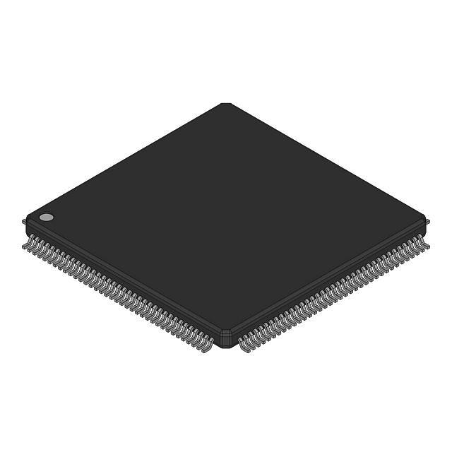


 工商网监
湘ICP备2023018690号
工商网监
湘ICP备2023018690号
