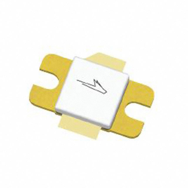
PTVA030121EA
Thermally-Enhanced High Power RF LDMOS FET
12 W, 50 V, 390 – 450 MHz
Description
The PTVA030121EA is an LDMOS FET characterized for use in
power amplifier applications in the 390 MHz to 450 MHz frequency
band. Features include high gain and a thermally-enhanced package.
Manufactured with Wolfspeed's advanced LDMOS process, this device
provides excellent thermal performance and superior reliability.
PTVA030121EA
Package H-36265-2
Features
CW Power Sweep
•
Unmatched input and output
•
Integrated ESD protection
•
Human Body Model Class 1C (per ANSI/ESDA/
JEDEC JS-001)
90
•
High gain, low thermal resistance
80
•
Excellent ruggedness
•
Capable of withstanding a 13:1 load mismatch at
50 V, 12 W, CW conditions
•
Pb-free and RoHS compliant
28
Gain (dB)
26
Gain
24
70
22
60
20
50
18
40
16
14
30
Efficiency
31
33
35
37
39
41
3-1
43
Drain Effficiency (%)
VDD = 50 V, IDQ = 30 mA, ƒ = 450 MHz
20
Output Power (dBm)
RF Characteristics
CW Measurements
VDD = 50 V, IDQ = 50 mA, POUT = 12 W, ƒ = 450 MHz
Characteristic
Symbol
Min
Typ
Max
Unit
Gain
Gps
23
25
—
dB
Drain Efficiency
hD
66
69
—
%
All published data at TCASE = 25°C unless otherwise indicated
ESD: Electrostatic discharge sensitive device—observe handling precautions!
Rev. 06, 2018-06-13
4600 Silicon Drive | Durham, NC 27703 | www.wolfspeed.com
�PTVA030121EA
2
DC Characteristics
Characteristic
Conditions
Symbol
Min
Typ
Max
Unit
Drain-Source Breakdown Voltage
VGS = 0 V, IDS = 1 mA
V(BR)DSS
105
—
—
V
Drain Leakage Current
VDS = 50 V, VGS = 0 V
IDSS
—
—
1.0
µA
VDS = 105 V, VGS = 0 V
IDSS
—
—
10.0
µA
On-State Resistance
VGS = 10 V, VDS = 0.1 V
RDS(on)
—
2.8
—
W
Operating Gate Voltage
VDS = 50 V, IDQ = 50 mA
VGS
—
3.6
—
V
Gate Leakage Current
VGS = 10 V, VDS = 0 V
IGSS
—
—
1.0
µA
Maximum Ratings
Parameter
Symbol
Value
Unit
Drain-Source Voltage
VDSS
105
V
Gate-Source Voltage
VGS
–6 to +12
V
Operating Voltage
VDD
0 to +55
V
Junction Temperature
TJ
225
°C
Storage Temperature Range
TSTG
–65 to +150
°C
Thermal Resistance (TCASE 70°C, 12 W CW)
RqJC
6.5
°C/W
Ordering Information
Type and Version
Order Code
Package and Description
Shipping
PTVA030121EA V1 R0
PTVA030121EA-V1-R0
H-36265-2, bolt-down
Tape & Reel, 50pcs
PTVA030121EA V1 R250
PTVA030121EA-V1-R250
H-36265-2, bolt-down
Tape & Reel, 250pcs
Rev. 06, 2018-06-13
4600 Silicon Drive | Durham, NC 27703 | www.wolfspeed.com
�3
PTVA030121EA
Typical Performance (data taken in a production test circuit)
CW Performance
CW Power Sweep
VDD = 50 V, IDQ = 30 mA
30
Gain
22
50
40
18
14
30
Efficiency
31
33
35
37
39
41
43
20
VDD = 50 V
VDD = 40 V
VDD = 30 V
60
22
50
18
40
14
10
30
Efficiency
30
32
34
36
38
40
42
a030121 3.3
44
20
Output Power (W)
CW Performance, Efficiency
CW Performance, Gain
VDD = 50 V, ƒ = 450 MHz, series show IDQ
VDD = 50 V, ƒ = 450 MHz, series show IDQ
30
80
Efficie
ency (%)
30 mA
22
IDQ = 0.5 mA
18
IDQ = 60 mA
IDQ = 30 mA
IDQ = 0.5 mA
70
60 mA
26
Ga
ain (dB)
70
Gain
26
Output Power (dBm)
14
80
Drain Efficiency (%)
70
60
26
10
34
Gain (dB)
30
80
Drain Effficiency (%)
450 MHz
420 MHz
390 MHz
34
Gain (dB)
IDQ = 30 mA, ƒ = 450 MHz, series show VDD
60
50
40
30
32
34
36
38
Output Power (dBm)
Rev. 06, 2018-06-13
40
42
20
32
34
36
38
40
42
Output Power (dBm)
4600 Silicon Drive | Durham, NC 27703 | www.wolfspeed.com
�PTVA030121EA
4
Broadband Circuit Impedance
Z Source Ω
Frequency
MHz
390
R
Z Load Ω
jX
R
jX
22.20
34.88
4.26
15.04
405
21.95
34.74
4.46
15.82
420
21.39
34.99
4.66
16.62
435
20.61
35.80
4.88
17.42
450
19.77
37.03
5.11
18.23
Reference Circuit
R808
2000 Ohm
S2
8
4
R802
6200 Ohm
In
NC
2
Out
NC
3
6
1
C802
1000 pF
7 5
R804
2000 Ohm
R801
1200 Ohm
R807
1200 Ohm
S3
S1
2
C
4
1
R806
1300 Ohm
R803
10 Ohm
3
S
B
3
E
TL115
R102
1000 Ohm
TL116
TL111
TL113 TL114
R805
2000 Ohm
TL101
εr=3.48
H=30 mil
RO/RO4350 B1
RF_IN
PORT
1
1
TL103
2
3
TL112
TL106
- v 1 _
BD
R101
2.2 Ohm
1 e a
C101
300 pF
TL107
TL102
0 1 2
TL104
a 0 3
TL105
- i n _ 1
0 - 1 3
- 2 0
1 1
C801
1000 pF
PORT
3
3
2
1
TL109
TL108
TL110
PORT
GATE DUT
2
L1
"5nH_D"
Reference circuit input schematic for ƒ = 450 MHz
Rev. 06, 2018-06-13
4600 Silicon Drive | Durham, NC 27703 | www.wolfspeed.com
�5
PTVA030121EA
Reference Circuit (cont.)
C204
1000000 pF
C205
300 pF
TL239
2
TL241
C203
10000000 pF
TL238
3
2
3
TL234
3
1
2
TL237
TL240
TL236
TL235
PORT
3
1
1
L3
"43nH_M"
TL215
TL224
TL222
TL204
TL203
TL223
TL233
TL242
DRAINPORT
DUT
1
TL216
TL213
TL214
TL206
TL207
TL210
L1
8 nH TL211
2
TL212
3
C202
300 pF TL209
TL225
TL208
1
2
TL205
TL202
C201
9.1 pF
L2
8 nH
TL201
TL230
TL227
1
3
a
0 3 0 1 2 1
TL218
e a - v
1 _ B
D- o u t
_ 1 0
- 1 3
- 2 0 1 1
TL228
PORT
RF_OUT
2
2
3
TL226
1
TL217
ε r=3.48
TL232
H=30 mil
RO/RO4350B1
TL229 TL231
TL221
TL219
TL220
Reference circuit output schematic for ƒ = 450 MHz
Reference Circuit Assembly
DUT
PTFA030121EA
Test Fixture Part No.
LTN/PTFA030121EA
Rogers RO4350, 0.508 mm [0.020”] thick, 1 oz. copper, εr = 3.48
Find Gerber files for this test fixture on the Wolfspeed Web site at (www.wolfspeed.com/RF
PCB
Electrical Characteristics at 450 MHz
Transmission
Electrical
Line
Characteristics
Dimensions: mm
Dimensions: mils
Input
TL101
0.009 l, 92.76 W
W = 0.51, L = 3.81
W = 20, L = 150
TL102
0.001 l, 45.29 W
W1 = 2.03, W2 = 2.03, W3 = 0.51
W1 = 80, W2 = 80, W3 = 20
TL103
0.001 l, 52.21 W
W = 1.63, L = 0.43
W = 64, L = 17
TL105
0.025 l, 52.21 W
W = 1.63, L = 10.13
W = 64, L = 39
TL106, TL109
0.003 l, 45.29 W
W = 2.03, L = 1.27
W = 80, L = 50
TL107
0.002 l, 45.29 W
W = 2.03, L = 0.76
W = 80, L = 30
TL110
0.013 l, 16.51 W
W = 7.62, L = 5.08
W = 300, L = 200
TL113
0.002 l, 92.76 W
W = 0.51, L = 1.02
W = 20, L = 40
TL115
0.013 l, 54.31 W
W = 1.52, L = 5.08
W = 60, L = 200
TL116
0.003 l, 54.31 W
W = 1.52, L = 1.02
W = 60, L = 40
table continued next page
Rev. 06, 2018-06-13
4600 Silicon Drive | Durham, NC 27703 | www.wolfspeed.com
�PTVA030121EA
6
Reference Circuit (cont.)
Electrical Characteristics at 450 MHz
Transmission
Electrical
Line
Characteristics
Dimensions: mm
Dimensions: mils
Output
TL201, TL202
0.005 l, 45.29 W
W = 2.03, L = 2.04
W = 80, L = 81
TL203
0.006 l, 38.92 W
W = 2.54, L = 2.54
W = 100, L = 100
TL206, TL207
0.029 l, 38.92 W
W = 2.54, L = 11.43
W = 100, L = 450
TL209
0.009 l, 38.92 W
W = 2.54, L = 3.56
W = 100, L = 140
TL210
0.018 l, 78.46 W
W = 0.76, L = 7.62
W = 30, L = 300
TL211
0.002 l, 25.11 W
W1 = 4.57, W2 = 4.57, W3 = 0.76
W1 = 180, W2 = 180, W3 = 30
TL212
0.003 l, 25.11 W
W = 4.57, L = 1.27
W = 180, L = 50
TL214
0.004 l, 25.11 W
W = 4.57, L = 1.52
W = 180, L = 60
TL215
0.010 l, 23.09 W
W = 5.08, L = 3.81
W = 200, L = 150
TL216
0.013 l, 16.51 W
W = 7.62, L = 5.08
W = 300, L = 200
TL217
0.018 l, 52.21 W
W = 1.63, L = 7.29
W = 64, L = 287
TL219
0.006 l, 52.21 W
W = 1.63, L = 2.41
W = 64, L = 95
TL222
0.006 l, 38.92 W
W = 2.54, L = 2.54
W = 100, L = 100
TL226
0.018 l, 52.21 W
W = 1.63, L = 7.34
W = 64, L = 289
TL227
0.002 l, 52.21 W
W = 1.63, L = 0.84
W = 64, L = 33
TL228
0.006 l, 52.21 W
W = 1.63, L = 2.30
W = 64, L = 91
TL229
0.006 l, 52.21 W
W = 1.63, L = 2.41
W = 64, L = 95
TL234
0.005 l, 27.14 W
W = 4.14, L = 2.12
W = 163, L = 84
TL235
0.014 l, 34.38 W
W = 3.02, L = 5.51
W = 119, L = 2 17
TL240
0.026 l, 61.53 W
W = 1.23, L = 10.63
W = 48, L = 419
TL241
0.010 l, 38.92 W
W1 = 2.54, W2 2.54, W3 = 4.14
W1 = 100, W2 = 100, W3 = 163
Rev. 06, 2018-06-13
4600 Silicon Drive | Durham, NC 27703 | www.wolfspeed.com
�PTVA030121EA
Production and Customer Circuit
PTVA030121EA
Reference Circuit (cont.)
RO4350, .030 (60)
RO4350, .030
C205
C204
R804
R808
PTFA 210452EF/LF
REFERENCE ON GRAPHIC:
a030121ea-v1_CD 10-13-2
(61)
C203
PCB
C801
R802 R807
R806
VDD
Heat SInk
C802
S1
R803
R805
L3
S3
S2
7
Metal
R801
R102
PCB
RF_OUT
RF_IN
L1
C101
C201
R101
L1 C202
Leads & Flange
L2
MWO Grey
PTVA030121_OUT
PTVA030121_IN
a 0 30 12 1e a- v 1 _ C D 0 6- 1 9- 2 01 8
Reference circuit assembly diagram (not to scale)
Component ID
Description
Suggested Supplier
P/N
C101
Chip capacitor, 300 pF
ATC
ATC100B301JW200XB
C801, C802
Capacitor, 1000 pF
Panasonic Electronic Components
ECJ-1VB1H102K
L1
Inductor, 5 nH
Coilcraft
A02TGLB
R101
Resistor, 2.2 W
Panasonic Electronic Components
ERJ-8GEYJ2R2V
R102
Resistor, 1000 W
Panasonic Electronic Components
ERJ-8GEYJ102V
R801, R807
Resistor, 1200 W
Panasonic Electronic Components
ERJ-3GEYJ122V
R802
Resistor, 6200 W
Panasonic Electronic Components
ERJ-8GEYJ622V
R803
Resistor, 10 W
Panasonic Electronic Components
ERJ-8GEYJ100V
R804, R805, R808
Resistor, 2000 W
Panasonic Electronic Components
ERJ-8GEYJ202V
R806
Resistor, 1300 W
Panasonic Electronic Components
ERJ-3GEYJ132V
S1
Transistor
Infineon Technologies
BCP56
S2
Voltage regulator
Fairchild Semiconductor
LM7805CT
S3
Potentiometer, 2K W
Bourns Inc.
3224W-1-202E
Input
table continued next page
Rev. 06, 2018-06-13
4600 Silicon Drive | Durham, NC 27703 | www.wolfspeed.com
�PTVA030121EA
8
Reference Circuit (cont.)
Component ID
Description
Suggested Supplier
P/N
C201
Chip capacitor, 9.1 pF
ATC
ATC100B9R1BW500XB
C202
Chip capacitor, 300 pF
ATC
ATC100B301JW200XB
C203
Chip capacitor, 10 µF
TDK Corporation
C5750X7S2A106M230KB
C204
Capacitor, 1 µF
TDK Corporation
C4532X7R2A105K230KA
C205
Chip capacitor, 300 pF
ATC
ATC100B301JW200XB
L1, L2
Inductor, 8 nH
Coilcraft
A03TGLB
L3
Inductor, 43 nH
Coilcraft
B10TGLB
Output
See next page for package mechanical specifications
Rev. 06, 2018-06-13
4600 Silicon Drive | Durham, NC 27703 | www.wolfspeed.com
�9
PTVA030121EA
Package Outline Specifications
Package H-36265-2
45° X 2.03
[.080]
6. ALL FOUR
CORNERS
2X 7.11
[.280]
2.66±.51
[.105±.020]
D
S
FLANGE
9.78
[.385]
3.05
[.120]
LID
10.16±.25
[.400±.010]
C
L
G
2X R1.52
[R.060]
C
L
4X R0.63
[R.025] MAX
SPH 1.57
[.062]
15.49±.51
[.610±.020]
4X R1.52
[R.060]
15.23
[.600]
10.16±.25
[.400±.010]
3.61±.38
[.142±.015]
h - 3 6 2 6 5 - 2 _ p o _ 0 9 - 0 8 - 2 0 1 1
1.02
[.040]
20.31
[.800]
6.
Rev. 06, 2018-06-13
Diagram Notes—unless otherwise specified:
Diagram Notes—unless otherwise specified:
1. Interpret dimensions and tolerances per ASME Y14.5M-1994.
1. Interpret dimensions and tolerances per ASME Y14.5M-1994.
2. Primary dimensions are mm. Alternate dimensions are inches.
2. Primary dimensions are mm. Alternate dimensions are inches.
3. All tolerances ± 0.127 [.005] unless specified otherwise.
3. All tolerances ±0.127 [0.005] unless specified otherwise.
4. Pins: D - drain, G - gate, S - source.
4. Pins: D – drain; G – gate; S – source
5. Lead thickness: 0.10 +0.051/–0.025 [.004 +.002/–.001].
5. Lead thickness: 0.10 + 0.051/–0.025 mm [0.004 + 0.002/–0.001 inch].
6. Exposed metal plane on top and bottom of ceramic insulator.
6. Exposed metal plane on top and bottom of ceramic insulator.
7. Gold plating thickness: 1.14 ± 0.38 micron [45 ± 15 microinch].
7. Gold plating thickness: 1.14 ± 0.38 micron [45 ± 15 microinch].
4600 Silicon Drive | Durham, NC 27703 | www.wolfspeed.com
�PTVA030121EA
10
Revision History
Revision
Date
Data Sheet Type
Page
Subjects (major changes since last revision)
01
2010-10-08
Advance
All
Data Sheet reflects advance specification for product development
02
2010-12-13
Advance
All
Change part number
03
2011-05-07
Preliminary
All
Change part number, update to Preliminary, add specifications
04
2011-11-10
Production
All
Data Sheet reflects released product specification
05
2013-07-02
Production
2
7, 8
Update DC Characteristics and Max Ratings table, add order codes
Add manufacturer
05.1
2016-04-19
Production
1, 2
Added ESD rating, updated ordering information
05.2
2017-02-02
Production
2
Updated operating voltage and junction temperature
06
2018-06-13
Production
All
Converted to Wolfspeed Data Sheet
For more information, please contact:
4600 Silicon Drive
Durham, North Carolina, USA 27703
www.wolfspeed.com/RF
Sales Contact
RFSales@wolfspeed.com
RF Product Marketing Contact
RFMarketing@wolfspeed.com
919.407.7816
Notes
Disclaimer
Specifications are subject to change without notice. Cree, Inc. believes the information contained within this data sheet
to be accurate and reliable. However, no responsibility is assumed by Cree for any infringement of patents or other rights
of third parties which may result from its use. No license is granted by implication or otherwise under any patent or patent rights of Cree. Cree makes no warranty, representation or guarantee regarding the suitability of its products for any
particular purpose. “Typical” parameters are the average values expected by Cree in large quantities and are provided for
information purposes only. These values can and do vary in different applications and actual performance can vary over
time. All operating parameters should be validated by customer’s technical experts for each application. Cree products
are not designed, intended or authorized for use as components in applications intended for surgical implant into the
body or to support or sustain life, in applications in which the failure of the Cree product could result in personal injury or
death or in applications for planning, construction, maintenance or direct operation of a nuclear facility.
Copyright © 2018 Cree, Inc. All rights reserved. The information in this document is subject to change without notice. Wolfspeed™ and the Wolfspeed logo are trademarks of Cree, Inc.
Rev. 06, 2018-06-13
www.wolfspeed.com
�