CGHV60170D
170 W, 6.0 GHz, 50V GaN HEMT Die
Description
Cree’s CGHV60170D is a gallium nitride (GaN) High Electron
Mobility Transistor (HEMT). GaN has superior properties
compared to silicon or gallium arsenide, including higher
breakdown voltage, higher saturated electron drift velocity,
and higher thermal conductivity. GaN HEMTs offer greater
power density and wider bandwidths compared to Si and
GaAs transistors.
PN: CGHV60170D
Features
Applications
•
•
•
•
•
•
•
•
•
•
•
•
18 dB Typical Small Signal Gain at 4 GHz
17 dB Typical Small Signal Gain at 6 GHz
65% Typical Power Added Efficiency
170 W Typical PSAT
50 V Operation
High Breakdown Voltage
Up to 6 GHz Operation
Broadband amplifiers
Tactical communications
Satellite communications
Industrial, Scientific, and Medical amplifiers
Class A, AB, Linear amplifiers suitable for OFDM,
W-CDMA, LTE, EDGE, CDMA waveforms
Packaging Information
•
•
Bare die are shipped in Gel-Pak® containers
Non-adhesive tacky membrane immobilizes die during shipment
Large Signal Models Available for ADS and MWO
Rev 1.1 – April 2020
4600 Silicon Drive | Durham, NC 27703 | wolfspeed.com
�CGHV60170D
2
Absolute Maximum Ratings (not simultaneous)
Parameter
Symbol
Rating
Units
Conditions
Drain source Voltage
VDSS
150
VDC
25˚C
Gate source Voltage
VGS
-10, +2
VDC
25˚C
Storage Temperature
TSTG
-65, +150
˚C
Operating Junction Temperature
TJ
225
˚C
Maximum Drain Current
IDMAX
12.6
A
25˚C
IMAX
20.8
mA
25˚C
Thermal Resistance, Junction to Case (packaged)
RθJC
1.36
˚C/W
85˚C, 83.2W Dissipation
Thermal Resistance, Junction to Case (die only)
RθJC
0.83
˚C/W
85˚C, 83.2W Dissipation
Mounting Temperature
TS
320
˚C
30 seconds
1
Maximum Forward Gate Current
2
Notes:
1
Current limit for long term, reliable operation
2
Eutectic die attach using 80/20 AuSn mounted to a 10 mil thick Cu15Mo85 carrier.
Electrical Characteristics (Frequency = 6 GHz unless otherwise stated; TC = 25˚C)
Characteristics
Symbol Min.
Typ.
Max.
Units Conditions
Gate Pinch-Off Voltage
VP
-3.8
-3.0
-2.3
V
VDS = 10 V, ID = 20.8 mA
Drain Current1
IDSS
16.8
20.8
–
A
VDS = 6 V, VGS = 2.0 V
Drain-Source Breakdown Voltage
VBD
125
–
–
V
VGS = -8 V, ID = 20.8 mA
On Resistance
RON
–
0.14
–
Ω
VDS = 0.1 V
Gate Forward Voltage
VG-ON
–
1.9
–
V
IGS = 20.8 mA
GSS
–
17
–
dB
VDD = 50 V, IDQ = 260 mA
Saturated Power Output
PSAT
–
170
–
W
VDD = 50 V, IDQ = 260 mA
Drain Efficiency4
η
–
65
–
%
VDD = 50 V, IDQ = 260 mA,= PSAT = 170 W
Intermodulation Distortion
IM3
–
-30
–
dBc
VDD = 50 V, IDQ = 260 mA, POUT = 170 W PEP
Output Mismatch Stress
VSWR
–
–
10 : 1
Y
No damage at all phase angles,
VDD = 50 V, IDQ = 260 mA, POUT = 170 W CW
Input Capacitance
CGS
–
28.3
–
pF
VDS = 50 V, Vgs = -8 V, f = 1 MHz
Output Capacitance
CDS
–
6.35
–
pF
VDS = 50 V, Vgs = -8 V, f = 1 MHz
Feedback Capacitance
CGD
–
0.6
–
pF
VDS = 50 V, Vgs = -8 V, f = 1 MHz
DC Characteristics
RF Characteristics
Small Signal Gain
2,3
Dynamic Characteristics
Notes:
1
Scaled from PCM data
2
PSAT is defined as IG = 2.0 mA
3
Pulsed 100 μsec, 10%
4
Drain Efficiency = POUT / PDC
Rev 1.1 – April 2020
4600 Silicon Drive | Durham, NC 27703 | wolfspeed.com
�CGHV60170D
3
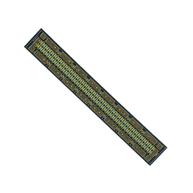
DIE Dimensions (units in microns)
Overall die size 820 x 5400 (+0/-50) microns, die thickness 100 microns.
All Gate and Drain pads must be wire bonded for electrical connection.
Assembly Notes:
•
Recommended solder is AuSn (80/20) solder. Refer to Cree’s website for the Eutectic Die Bond Procedure
application note at www.cree.com/rf/document-library
•
•
•
•
•
•
Vacuum collet is the preferred method of pick-up
The backside of the die is the Source (ground) contact
Die back side gold plating is 5 microns thick minimum
Thermosonic ball or wedge bonding are the preferred connection methods
Gold wire must be used for connections
Use the die label (XX-YY) for correct orientation
Electrostatic Discharge (ESD) Classifications
Parameter
Symbol
Class
Test Methodology
Human Body Model
HBM
1A (> 250 V)
JEDEC JESD22 A114-D
Charge Device Model
CDM
2 (125 V to 250 V)
JEDEC JESD22 C101-C
Rev 1.1 – April 2020
4600 Silicon Drive | Durham, NC 27703 | wolfspeed.com
�CGHV60170D
4
Typical Performance
Figure 1. CGHV60170D Output Power, Gain and Efficiency vs. Input Power at Tcase = 25°C
VDD = 50 V, IDQ = 260 mA, Frequency = 2.7 GHz
Gain (dB)
Power (dBm) and Eff (%)
CW Transfer
Power (dBm)
Figure 2. CGHV60170D GMAX and K Factor vs. Frequency at Tcase = 25°C
VDD = 50 V, IDQ = 260 mA
K-Factor
Gmax (dB)
Gmax & K-Factor
Frequency (MHz)
Rev 1.1 – April 2020
4600 Silicon Drive | Durham, NC 27703 | wolfspeed.com
�CGHV60170D
5
Typical Die S-Parameters (Small Signal, VDS = 50 V, IDQ = 260 mA, magnitude / angle)
Frequency
Mag S11
Ang S11
Mag S21
Ang S21
Mag S12
Ang S12
Mag S22
Ang S22
0.5
0.943
-168.72
9.039
75.28
0.009
-13.64
0.544
-156.15
0.6
0.946
-170.27
7.375
70.86
0.009
-17.83
0.571
-155.58
0.7
0.948
-171.36
6.170
66.84
0.009
-21.63
0.600
-155.23
0.8
0.951
-172.18
5.255
63.13
0.009
-25.12
0.627
-155.11
0.9
0.953
-172.81
4.538
59.69
0.008
-28.34
0.654
-155.19
1
0.956
-173.33
3.961
56.48
0.008
-31.32
0.680
-155.45
1.1
0.959
-173.76
3.488
53.50
0.008
-34.08
0.704
-155.84
1.2
0.961
-174.13
3.095
50.72
0.008
-36.64
0.726
-156.32
1.3
0.963
-174.45
2.764
48.12
0.007
-39.02
0.747
-156.87
1.4
0.966
-174.73
2.482
45.69
0.007
-41.22
0.766
-157.45
1.5
0.968
-174.99
2.239
43.42
0.007
-43.27
0.783
-158.07
1.6
0.970
-175.23
2.030
41.30
0.007
-45.17
0.799
-158.69
1.7
0.971
-175.44
1.848
39.31
0.006
-46.94
0.814
-159.31
1.8
0.973
-175.64
1.688
37.44
0.006
-48.59
0.827
-159.93
1.9
0.974
-175.83
1.548
35.68
0.006
-50.12
0.839
-160.53
2
0.976
-176.00
1.424
34.02
0.006
-51.55
0.850
-161.11
2.1
0.977
-176.17
1.314
32.47
0.005
-52.88
0.860
-161.68
2.2
0.978
-176.32
1.216
31.00
0.005
-54.13
0.869
-162.23
2.3
0.979
-176.46
1.128
29.60
0.005
-55.30
0.877
-162.76
2.4
0.980
-176.60
1.049
28.29
0.005
-56.39
0.885
-163.27
2.5
0.981
-176.73
0.977
27.04
0.005
-57.41
0.892
-163.75
2.6
0.982
-176.85
0.913
25.85
0.005
-58.37
0.898
-164.22
2.7
0.983
-176.97
0.855
24.72
0.004
-59.27
0.904
-164.67
2.8
0.984
-177.08
0.802
23.65
0.004
-60.11
0.909
-165.09
2.9
0.984
-177.18
0.753
22.63
0.004
-60.91
0.914
-165.50
3
0.985
-177.29
0.709
21.65
0.004
-61.66
0.919
-165.90
3.2
0.986
-177.47
0.631
19.82
0.004
-63.03
0.927
-166.63
3.4
0.987
-177.65
0.566
18.13
0.004
-64.25
0.934
-167.31
3.6
0.988
-177.81
0.510
16.57
0.003
-65.34
0.940
-167.93
3.8
0.989
-177.95
0.462
15.12
0.003
-66.31
0.945
-168.50
4
0.989
-178.09
0.420
13.78
0.003
-67.19
0.950
-169.02
4.2
0.990
-178.22
0.384
12.51
0.003
-67.97
0.954
-169.51
4.4
0.991
-178.34
0.352
11.32
0.003
-68.67
0.958
-169.96
4.6
0.991
-178.45
0.324
10.20
0.003
-69.30
0.961
-170.38
4.8
0.991
-178.56
0.299
9.14
0.002
-69.86
0.964
-170.77
5
0.992
-178.66
0.277
8.13
0.002
-70.36
0.966
-171.14
5.2
0.992
-178.76
0.258
7.18
0.002
-70.81
0.968
-171.48
5.4
0.992
-178.85
0.240
6.26
0.002
-71.20
0.970
-171.80
5.6
0.993
-178.94
0.224
5.38
0.002
-71.55
0.972
-172.10
5.8
0.993
-179.02
0.210
4.54
0.002
-71.85
0.974
-172.38
6
0.993
-179.10
0.197
3.73
0.002
-72.10
0.975
-172.65
To download the s-parameters in s2p format, go to the CGHV60170D Product Page and click on the documentation tab.
Rev 1.1 – April 2020
4600 Silicon Drive | Durham, NC 27703 | wolfspeed.com
�CGHV60170D
6
Part Number System
CGHV60170D
Die
Power Output (W)
Upper Frequency (GHz)
Cree GaN High Voltage
Table 1.
Parameter
Value
Units
Upper Frequency1
6.0
GHz
Power Output
170
W
Package
Bare Die
-
Note1: Alpha characters used in frequency code indicate a value
greater than 9.9 GHz. See Table 2 for value.
Table 2.
Rev 1.1 – April 2020
Character Code
Code Value
A
0
B
1
C
2
D
3
E
4
F
5
G
6
H
7
J
8
K
9
Examples:
1A = 10.0 GHz
2H = 27.0 GHz
4600 Silicon Drive | Durham, NC 27703 | wolfspeed.com
�CGHV60170D
7
Product Ordering Information
Order Number
Description
Unit of Measure
CGHV60170D
GaN HEMT Bare Die
Each
Rev 1.1 – April 2020
4600 Silicon Drive | Durham, NC 27703 | wolfspeed.com
�CGHV60170D
8
For more information, please contact:
4600 Silicon Drive
Durham, North Carolina, USA 27703
www.wolfspeed.com/RF
Sales Contact
RFSales@cree.com
Notes
Disclaimer
Specifications are subject to change without notice. “Typical” parameters are the average values expected by Cree in
large quantities and are provided for information purposes only. Cree products are not warranted or authorized for use
as critical components in medical, life-saving, or life-sustaining applications, or other applications where a failure would
reasonably be expected to cause severe personal injury or death. No responsibility is assumed by Cree for any infringement of patents or other rights of third parties which may result from use of the information contained herein. No license
is granted by implication or otherwise under any patent or patent rights of Cree.
© 2014-2020 Cree, Inc. All rights reserved. Wolfspeed® and the Wolfspeed logo are registered trademarks of Cree, Inc.
Rev 1.1 – April 2020
4600 Silicon Drive | Durham, NC 27703 | wolfspeed.com
�