TS5213
Taiwan Semiconductor
80mA Low Noise LDO Voltage Regulator
with Enable Function
GENERAL DESCRIPTION
FEATURES
TS5213 is an efficient linear voltage regulator with ultra-
●
Ultra Low Noise Output
low noise output, very low dropout voltage (typically
●
Output Current up to 80mA
50mV at light loads and 320mV at 80mA), and very low
●
Low Power Consumption
ground current (225μA at 20mA), providing high output
●
“Zero” Off-mode Consumption
current even when the application requires very low
●
Logic Controlled Electronic Enable
dropout voltage. The Chip Enable (EN) includes a
●
Current Limit & Thermal Shutdown Protection
CMOS or TTL compatible input allows the output to be
turned off to prolong battery life. When shutdown,
APPLICATION
power consumption drops nearly to zero. TS5213 is
●
Cellular Telephones
included a precision voltage reference, error correction
●
Palmtops, Notebook Computers
circuit, a current limited output driver, over temperature
●
Battery Powered Equipment
shutdown and revered battery protection.
●
SMPS Post Regulator and DC to DC Modules
●
High-efficiency Linear Power Supplies
●
Portable Application
Pin Definition:
1. Input
2. Ground
3. Enable
4. N/C
5. Output
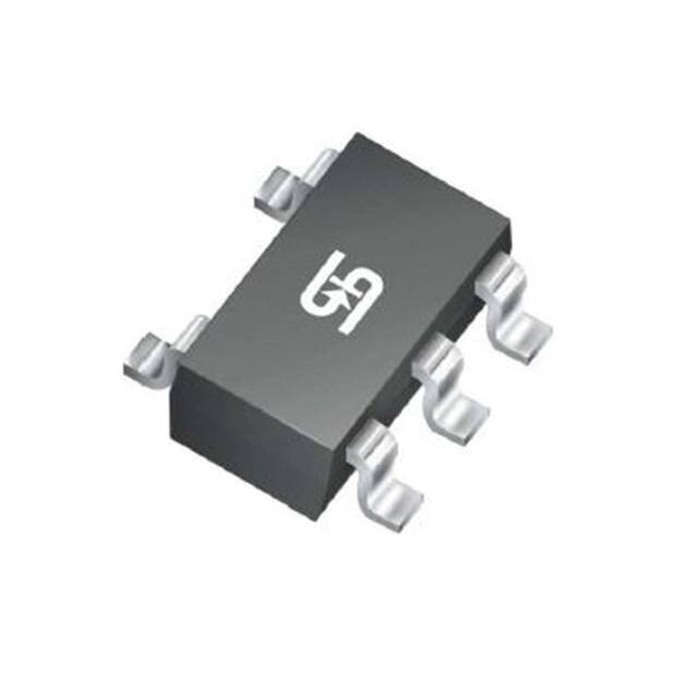
SOT-25
Notes: Moisture sensitivity level: level 3. Per J-STD-020
TYPICAL APPLICATION CIRCUIT
EN may be connected to VIN pin to regulation ON
CIN > 0.1μF in basic operating
COUT >0.47μF in low noise operating
Document Number: DS_P0000201
1
Version: G15
�TS5213
Taiwan Semiconductor
ABSOLUTE MAXIMUM RATINGS (TA = 25°C unless otherwise noted) (Note 1)
PARAMETER
SYMBOL
LIMIT
UNIT
Input Supply Voltage
VIN
-20~ +20
V
Enable Input Voltage
VCE
-20~ +20
V
Power Dissipation (Note 2)
PD
Internal limited
RθJA
220
TJ
-40 ~ +125
o
-65 ~ +150
o
Thermal Resistance
Operating Junction Temperature Range
Storage Temperature Range
TSTG
o
Lead Soldering Temperature (260 C)
o
C/W
C
C
5
S
SYMBOL
LIMIT
UNIT
Input Supply Voltage
VIN
+2.5 ~ +16
V
Enable Input Voltage
VCE
0 ~ VIN
V
RECOMMEND OPERATING RATING
(Note 2)
PARAMETER
ELECTRICAL SPECIFICATIONS
(VIN = VO+1V, IO = 100μA, COUT = 1μF, Vce≥2V, TA = 25°C unless otherwise noted)
PARAMETER
CONDITIONS
MIN
TYP
MAX
UNIT
VIN=VO + 1V
-3
--
3
%
-40ºC ≤ TJ ≤ +125ºC
-4
--
4
Output Voltage Temp. Coefficient
(Note 5)
--
50
200
ppm/ C
Line Regulation
VO+1V ≤ VIN ≤ 16V
--
0.008
0.3
%
0.1mA ≤ Io ≤ 80mA
--
0.08
0.3
%
IO=100uA
--
50
--
IO=20mA
--
230
300
IO=50mA
--
280
370
IO=80mA
--
320
420
VEN ≤0.4V (shutdown)
--
0.01
10
IO=100μA
--
80
--
VEN≥2V
IO=20mA
--
225
750
(active)
IO=50mA
--
850
--
IO=80mA
--
1800
3000
Output Voltage
Load Regulation
Dropout Voltage
(Note 6)
(Note 7)
Quiescent Current
Ground Pin Current
(Note 8)
o
mV
μA
μA
Output Current Limit
VOUT =0V
--
250
500
mA
Power Supply Rejection Ratio
At f=100Hz, IO=100μA,
--
65
--
dB
--
0.05
--
%/W
Thermal Regulation
(Note 9)
Document Number: DS_P0000201
2
Version: G15
�TS5213
Taiwan Semiconductor
ELECTRICAL SPECIFICATIONS
(VIN = VO+1V, IO = 100μA, COUT = 1μF, Vce≥2V, TA = 25°C unless otherwise noted)
Enable Function
PARAMETER
CONDITIONS
Enable Input Logic-Low Voltage
Regulation shutdown
Enable Input Logic-High Voltage
Regulation enable
Enable Input Current
VIL≤ 0.6V
VIH≥ 2.0V
MIN
TYP
MAX
UNIT
--
--
0.6
V
2.0
--
--
V
---
0.01
15
1
50
μA
V
Note:
1. Exceeding the absolute maximum rating may damage the device.
2. The maximum allowable power dissipation at any TA is PD(MAX) = [TJ(MAX) - Ta] + RθJA. Exceeding the maximum allowable
power dissipation will result in excessive die temperature, and the regulator will go into thermal shutdown.
3. Devices are ESD sensitive. Handling precautions recommended.
4. The device is not guaranteed to function outside its operating rating.
5. Output voltage temperature coefficient is defined as the worst case voltage change divided by the total temperature range.
6. Regulation is measured at constant junction temperature using low duty cycle pulse testing. Parts are tested for load
regulation in the load range from 1mA to 80mA. Changes in output voltage due to heating effects are covered by the
thermal regulation specification.
7. Dropout voltage is defined as the input to output differential at which the output voltage drops 2% below its nominal value
measured at 1V differential.
8. Ground pin current is the regulator quiescent current plus pass transistor base current. The total current drawn from the
supply is the sum of the load current plus the ground pin current.
9. Thermal regulation is defined as the change in output voltage at a time “t” after a change in power dissipation is applied,
excluding load or line regulation effects. Specifications are for a 80mA load pulse at VIH =16V for t=10ms.
Document Number: DS_P0000201
3
Version: G15
�TS5213
Taiwan Semiconductor
ORDERING INFORMATION
OUTPUT VOLTAGE
PART NO.
PACKAGE
PACKING
3,000pcs / 7” Reel
3.3V
TS5213CX533 RFG
SOT-25
5V
TS5213CX550 RFG
SOT-25
3,000pcs / 7” Reel
Note:
1. Compliant to RoHS Directive 2011/65/EU and in accordance to WEEE 2002/96/EC.
2. Halogen-free according to IEC 61249-2-21 definition.
BLOCK DIAGRAMS
APPLICATION INFORMATION
Enable Input
TS5213 series feature an active-high (>2V) enable (EN) input that allows ON/OFF control of the regulator.
Current drain reduces to “zero” when the device is shutdown, with only micro-amperes of leakage current. The
EN is compatible with CMOS logic interfacing. EN may be directly tied to VIH and pulled up to the maximum
supply voltage.
Input Capacitor Requirement
An input capacitor of 0.17μF or greater is recommended when the device is more than 10” away from the bulk
AC supply capacitance or when the supply is a battery.
Output Capacitor Requirement
The TS5213 series requires an output capacitor to maintain stability and improve transient response is necessary.
The TS5213 is ultra-stable, requiring only 0.47uF of output capacitance for stability. It is stable with all type of
capacitors, including the tiny, low-ESR ceramic chip capacitors. The output capacitor value may be increased
without limit.
No Load Stability
The TS5213 series will remain stable and in regulation with no load, unlike many other voltage regulators. This is
especially important in CMOS RAM keep alive applications.
Document Number: DS_P0000201
4
Version: G15
�TS5213
Taiwan Semiconductor
APPLICATION INFORMATION (CONTINUE)
Thermal Characteristics
TS5213 series is designed to provide 80mA of continuous current in a very small package. Maximum power
dissipation can be calculated based on the output current and the voltage drop across the part. To determine the
maximum power dissipation of the package, use the junction-ambient thermal resistance of the device and the
following basic equation:
PD(MAX) = [ TJ(MAX) – T A ] /ΘJA
o
TJ(MAX) is the maximum junction temperature of the die(125 C), and Ta is the ambient operating temperature. ΘJA
is layout dependent, the actual power dissipation of the regulator circuit can be determined using the equation:
PD = (VIN – VOUT) * IOUT + VIN * IGND
Substituting PD(MAX) for PD and solving for the operating conditions that are critical to the application will give the
maximum operating conditions for the regulator circuit. For example, when operating the TS5213CX550 at room
temperature with a minimum footprint layout, the maximum input voltage for a set output current can be
determined as follows:
o
o
o
PD(MAX) = (125 C – 25 C) / 220 C/W
PD(MAX) = 455mW
o
The junction to ambient thermal resistance for the minimum footprint is 220 C/W, the maximum power dissipation
must not be exceeded for proper operation. Using the output voltage of 5.0V and an output current of 80mA, the
maximum input voltage can be determined. Form the electrical characteristics table, the maximum ground
current for 80mA output current is 1mA.
445mW = (VIN – 5.0V ) * 80mA + VIN * 1.8mA
445mW = VIN * 80mA – 5.0 * 80mA + VIN * 1.8mA
445mW = VIN * 80mA – 400mW + VIN * 1.8mA
845mW = VIN * 81.8mA
VIN (max) = 10.33V
Therefore, a 5.0V application at 80mA of output current can accept a maximum input voltage of 10.33V in a SOT25 package.
Document Number: DS_P0000201
5
Version: G15
�TS5213
Taiwan Semiconductor
CHARACTERISTICS CURVES
(TC = 25°C unless otherwise noted)
Figure 1. Output Voltage vs. Input Voltage
Figure 2. Ground Current vs. Output Current
Figure 3. Dropout Voltage vs. Output Current
Figure 4. Short Circuit Current vs. Input
Voltage
Figure 5. Ripple Rejection vs. Frequency
Figure 6. Ripple Rejection vs. Frequency
Document Number: DS_P0000201
6
Version: G15
�TS5213
Taiwan Semiconductor
PACKAGE OUTLINE DIMENSIONS (Unit: Millimeters)
SOT-25
SUGGESTED PAD LAYOUT (Unit: Millimeters)
MARKING DIAGRAM
T
X
Y
M
= Device Code
= Voltage Code (5 = 5.0V, S = 3.3V)
= Year Code
= Month Code for Halogen Free Product
O =Jan P =Feb Q =Mar R =Apr
S =May T =Jun U =Jul
V =Aug
W =Sep X =Oct
Y =Nov Z =Dec
L = Lot Code (1~9, A~Z)
Document Number: DS_P0000201
7
Version: G15
�TS5213
Taiwan Semiconductor
Notice
Specifications of the products displayed herein are subject to change without notice. TSC or anyone on its behalf,
assumes no responsibility or liability for any errors or inaccuracies.
Information contained herein is intended to provide a product description only. No license, express or implied, to
any intellectual property rights is granted by this document. Except as provided in TSC’s terms and conditions of
sale for such products, TSC assumes no liability whatsoever, and disclaims any express or implied warranty,
relating to sale and/or use of TSC products including liability or warranties relating to fitness for a particular purpose,
merchantability, or infringement of any patent, copyright, or other intellectual property right.
The products shown herein are not designed for use in medical, life-saving, or life-sustaining applications.
Customers using or selling these products for use in such applications do so at their own risk and agree to fully
indemnify TSC for any damages resulting from such improper use or sale.
Document Number: DS_P0000201
8
Version: G15
�


 工商网监
湘ICP备2023018690号
工商网监
湘ICP备2023018690号
