TS39104CS
Taiwan Semiconductor
1A Ultra Low Dropout Voltage Regulator
with Multi-Functions
DESCRIPTION
FEATURES
The TS39104 are 1A ultra low dropout linear voltage
regulators that provide low voltage, high current output
from an extremely small package. This regulator offers
extremely low dropout (typically 400mV at 1A) and
very low ground current (typically 12mA at 1A).
The TS39104 are fully protected against over current
faults, reversed input polarity, reversed lead insertion,
over temperature operation, positive and negative
transient voltage spikes, logic level enable control and
error flag which signals whenever the output falls out
of regulation.
On the TS39104, the enable pin may be tied to Vin if it
●
●
●
●
●
●
is not required for enable control.
●
●
●
●
●
●
●
en
de
d
Dropout voltage typically 400mV @ Io=1A
Output Current up to 1A
Low Ground Current
Extremely Fast Transient Response
Reversed Leakage & Reverse Battery Protection
Current Limit Protection
●
Thermal Shutdown Protection
●
Compliant to RoHS Directive 2011/65/EU and in
accordance to WEEE 2002/96/EC.
●
Halogen-free according to IEC 61249-2-21
APPLICATION
eco
mm
ULDO Linear Regulator for PC add-in Cards
TM
PowerPC Power Supplies
Battery Powered Equipment
Consumer and Personal Electronics
High Efficiency Linear Power Supplies
SMPS Post Regulator and DC to DC Modules
High-efficiency Post Regulator for Switching
Supply
Portable Application
Low-Voltage microcontrollers and Digital Logic
No
tR
●
●
SOP-8
Pin Definition:
1. Enable
2. Input
3. Feedback
4. Output
8. Ground
7. Ground
6. Ground
5. Ground
Note: MSL 3 (Moisture Sensitivity Level) per J-STD-020
TYPICAL APPLICATION CIRCUIT
1
Version: D1706
�TS39104CS
Taiwan Semiconductor
ABSOLUTE MAXIMUM RATINGS (Note 1)
PARAMETER
SYMBOL
LIMIT
UNIT
Supply Voltage
VIN
-20V ~ +20
V
Enable Voltage
VEN
+20
V
Storage Temperature Range
TSTG
-65 ~ +150
°C
5
s
CONDITIONS
UNIT
+2.25 ~ +16
V
Lead Soldering Temperature (260°C)
RECOMMENDED OPERATING CONDITIONS
(Note 3)
d
SYMBOL
Operation Input Voltage
VIN
Operation Enable Voltage
de
PARAMETER
Power Dissipation (Note 4)
+2.25 ~ +16
V
PD
Internally Limited
W
TJ
-40 ~ +125
°C
RJC
20
en
Operating Junction Temperature Range
VEN
Thermal Resistance Junction to Case
mm
ELECTRICAL SPECIFICATIONS
°C/W
VIN=VOUT+1V, VIN=2.5V for fixed reference output voltage, Venable=2.25V, TA=25°C, unless otherwise specified
PARAMETER
CONDITIONS
IL=10mA
Line Regulation
Load Regulation
10mA IL 1.0A,
2.5V VIN 16V
IL=10mA, Vo+1V VIN 16V
VIN =Vout+1V, 8mAIL300mA
VIN =Vout+1V, 10mAIL1A
tR
Output Voltage Temp. Coefficient
(Note 5)
(Note 6)
No
Dropout Voltage
Quiescent Current
Current Limit
Adjust Pin Bias Current
Reference Voltage Temp. Coefficient
Adjust Pin Bias Current Temp.
Coefficient
TYP
1.215
e co
Reference Output Voltage
MIN
IL=100mA
ΔVOUT = -1%
IL=500mA
IL=1A
IL=100mA
VIN= VOUT +1V IL=500mA
IL=1A
VOUT =0, VIN = VOUT +1V
(Note 8)
1.203
MAX
UNIT
1.265
1.24
1.277
--------------
0.05
0.05
0.2
40
100
275
400
0.7
4
12
1.8
40
20
0.5
0.1
1.0
100
250
350
630
2
6
20
-120
--
--
0.1
--
-2.25
---
-----
0.8
-75
4
mA
%
%
ppm/°C
mV
mA
A
nA
ppm/°C
nA/°C
Enable Input
Input Logic Voltage
Enable Pin Input Current
Low (OFF)
High (ON)
VEN =2.25V
VEN =0.8V
2
V
µA
Version: D1706
�TS39104CS
Taiwan Semiconductor
ELECTRICAL SPECIFICATIONS (Continue)
ORDERING INFORMATION
mm
en
de
d
Note:
1. Absolute Maximum Rating is limits beyond which damage to the device may occur. For guaranteed
specifications and test conditions see the Electrical Characteristics.
2. The device is not guaranteed to operate outside its operating rating.
3. Devices are ESD sensitive. Handling precautions recommended.
4. The maximum allowable power dissipation is a function of the maximum junction temperature, T J, the junction
to ambient thermal resistance, RӨJA, and the ambient temperature, T A. Exceeding the maximum allowable
power dissipation will cause excessive die temperature, and the regulator will go into thermal shutdown. The
effective value of RӨJA can be reduced by using a heat sink, PD(max) = (TJ(max) – TA) / RӨJA
5. Dropout voltage is defined as the input to output differential at which the output voltage drops -1% below its
nominal value measured at 1V differential.
6. Ground pin current is the regulator quiescent current. The total current drawn from the source is the sum of the
ground pin current and output load current, IGND = IIN - IOUT for fix output voltage, , IGND = IIN - IOUT +10mA for fix
reference output voltage in full load regulation.
7. VREF VOUT (VIN – 1V), 2.25V VIN 16V, 10mA IL 1A.
o
8. Output voltage temperature coefficient is ΔVOUT (worse cast) / (TJ(max) – TJ(MIN)) where is TJ(max) +125 C and
o
TJ(MIN) is 0 C.
9. For adjustable device and fixed device with VOUT > 2.25V
PACKAGE
PACKING
TS39104CS RLG
SOP-8
2,500pcs / 13”Reel
No
tR
e co
PART NO.
3
Version: D1706
�TS39104CS
Taiwan Semiconductor
de
d
BLOCK DIAGRAM
en
PIN DESCRIPTION
NAME
FUNCTION
TTL/COMS compatible input. Logic high is enable; logic low or open is shutdown
1
Enable
2
Input
3
Adjustable
4
Output
Regulator output
5,6,7,8
Ground
Ground pin
mm
PIN NO.
Unregulated input: +16V maximum supply
e co
Adjustable input: Feedback input. Connect to resistive voltage-divider network.
APPLICATION INFORMATION
The TS39104 is a high performance with low dropout voltage regulator suitable for moderate to high current and
voltage regulator application. Its 630mV dropout voltage at full load and over temperature makes it especially
tR
valuable in battery power systems and as high efficiency noise filters in post regulator applications. Unlike normal
NPN transistor design, where the base to emitter voltage drop and collector to emitter saturation voltage limit the
minimum dropout voltage, dropout performance of the PNP output of these devices is limited only by low V CE
saturation voltage.
No
The TS39104 s fully protected from damage due to fault conditions. Linear current limiting is provided. Output
current during overload conditions is constant. Thermal shutdown the device when the die temperature exceeds
the maximum safe operating temperature. Transient protection allows device survival even when the input voltage
spikes above and below nominal. The output structure of these regulators allows voltages in excess of the desired
output voltage to be applied without reverse current flow
Input Capacitor Requirement
An input capacitor of 1µF or greater is recommended when the device is more than 4” away from the bulk AC
supply capacitance or when the supply is a battery. Small, surface mount, ceramic chip capacitors can be used for
bypassing. Larger values will help to improve ripple rejection by bypassing the input to the regulator, further
improving the integrity of the output voltage.
Minimum Load Current
The TS39104 is specified between finite loads. If the output current is too small leakage currents dominate and the
output voltage rises. A 10mA minimum load current is necessary for proper regulation.
4
Version: D1706
�TS39104CS
Taiwan Semiconductor
APPLICATION INFORMATION (Continue)
Output Capacitor Requirement
The TS39104 requires an output capacitor to maintain stability and improve transient response is necessary. The
value of this capacitor is dependent upon the output current, lower currents allow smaller capacitors. TS39104
output capacitor selection is dependent upon the ESR of the output capacitor to maintain stability. When the output
capacitor is 10µF or greater, the output capacitor should have an ESR less than 2Ω. This will improve transient
response as well as promote stability. Ultra low ESR capacitors (
很抱歉,暂时无法提供与“TS39104CS RLG”相匹配的价格&库存,您可以联系我们找货
免费人工找货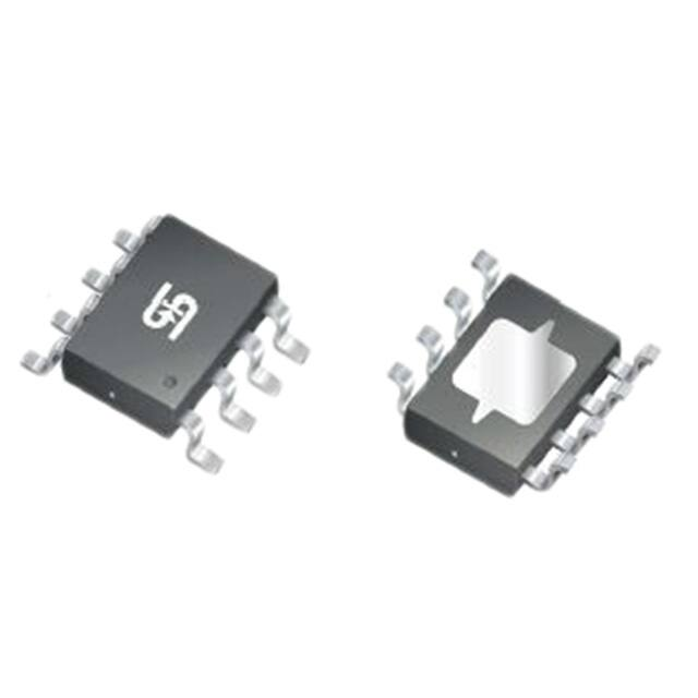


 工商网监
湘ICP备2023018690号
工商网监
湘ICP备2023018690号
