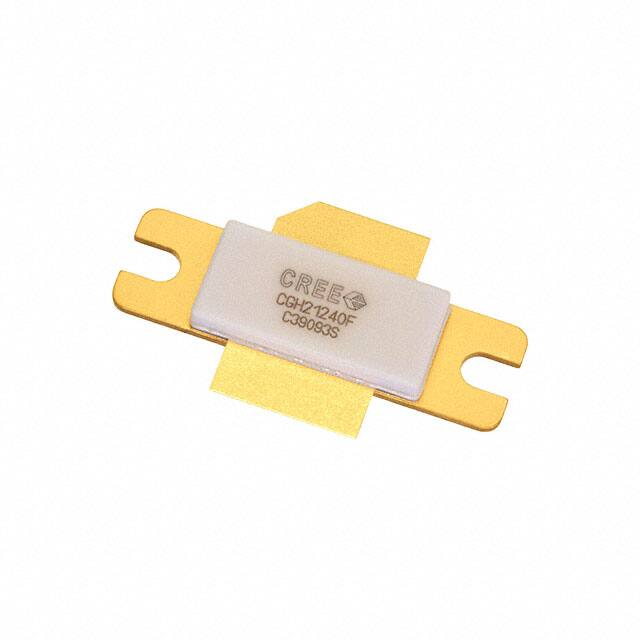
CGH21240F
240 W, 1.8 - 2.3 GHz, GaN HEMT for WCDMA, LTE,
WiMAX
Description
Cree’s CGH21240F is a gallium nitride (GaN) high electron mobility
transistor (HEMT) designed specifically with high efficiency,
high gain and wide bandwidth capabilities, which makes the
CGH21240F ideal for 1.8-2.3 GHz WCDMA and LTE amplifier
applications. The transistor is supplied in a ceramic/metal flange
package.
Package Types: 440117
PN: CGH21240F
Typical Performance Over 2.0-2.3 GHz (TC = 25˚C) of Demonstration Amplifier
Parameter
2.0 GHz
2.1 GHz
2.2 GHz
2.3 GHz
Units
Gain @ 46 dBm
13.1
14.6
15.1
15.7
dB
ACLR @ 46 dBm
-36.5
-34.5
-34.2
-32.0
dBc
Drain Efficiency @ 46 dBm
30.5
32.7
32.9
33.8
%
Note: Measured in the CGH21240F-AMP amplifier circuit, under WCDMA 3GPP test model 1, 64 DPCH, 67% clipping, PAR = 8.81 dB @ 0.01 % Probability on CCDF
Features
•
•
•
•
•
1.8 - 2.3 GHz Operation
15 dB Gain
-35 dBc ACLR at 40 W PAVE
33% Efficiency at 40 W PAVE
High Degree of DPD Correction Can be Applied
Large Signal Models Available for ADS and MWO
Rev 3.1 – March 2020
4600 Silicon Drive | Durham, NC 27703 | wolfspeed.com
�CGH21240F
2
Absolute Maximum Ratings (not simultaneous) at 25˚C Case Temperature
Parameter
Symbol
Rating
Units
Conditions
Drain-Source Voltage
VDSS
120
Volts
25˚C
Gate-to-Source Voltage
VGS
-10, +2
Volts
25˚C
Power Dissipation
PDISS
115
Watts
Storage Temperature
TSTG
-65, +150
˚C
Operating Junction Temperature
TJ
225
˚C
Maximum Forward Gate Current
IGMAX
60
mA
25˚C
Maximum Drain Current
IDMAX
24
A
25˚C
Soldering Temperature2
TS
245
˚C
Screw Torque
τ
40
in-oz
Thermal Resistance, Junction to Case3
RθJC
0.75
˚C/W
Case Operating Temperature
TC
-40, +150
˚C
1
3
85˚C
Notes:
1
Current limit for long term, reliable operation
2
Refer to the Application Note on soldering at wolfspeed.com/RF/Document-Library
3
Measured for the CGH21240F at PDISS = 115 W
Electrical Characteristics (TC = 25˚C)
Characteristics
Symbol
Min.
Typ.
Max.
Units
Conditions
Gate Threshold Voltage
VGS(th)
-3.8
-3.0
-2.3
VDC
VDS = 10 V, ID = 57.6 mA
Gate Quiescent Voltage
VGS(Q)
–
-2.7
–
VDC
VDS = 28 V, ID = 1.0 mA
Saturated Drain Current
IDS
46.4
56.0
–
A
VDS = 6.0 V, VGS = 2.0 V
Drain-Source Breakdown Voltage
VBR
84
–
–
VDC
VGS = -8 V, ID = 57.6 mA
Saturated Output Power3,4
Psat
–
215
–
W
VDD = 28 V, IDQ = 1.0 A
Pulsed Drain Efficiency3
η
–
65
–
%
VDD = 28 V, IDQ = 1.0 A, POUT = PSAT
Modulated Gain
Gss
13.5
15
–
dB
VDD = 28 V, IDQ = 1.0 A, POUT = 46 dBm
ACLR
–
-35
-30
dBc
VDD = 28 V, IDQ = 1.0 A, POUT = 46 dBm
Modulated Drain Efficiency
η
27
33
–
%
VDD = 28 V, IDQ = 1.0 A, POUT = 46 dBm
Output Mismatch Stress
VSWR
–
–
10 : 1
Y
No damage at all phase angles,
VDD = 28 V, IDQ = 1.0 A, POUT = 40 W CW
CGS
–
172
–
pF
VDS = 28 V, Vgs = -8 V, f = 1 MHz
Output Capacitance
CDS
–
19.5
–
pF
VDS = 28 V, Vgs = -8 V, f = 1 MHz
Feedback Capacitance
CGD
–
3.2
–
pF
VDS = 28 V, Vgs = -8 V, f = 1 MHz
DC Characteristics
1
RF Characteristics (TC = 25˚C, F0 = 2.14 GHz unless otherwise noted)
2,3
6
WCDMA Linearity
6
6
Dynamic Characteristics
Input Capacitance7
7
Notes:
1
Measured on wafer prior to packaging
2
Scaled from PCM data
3
Pulse Width = 40 μS, Duty Cycle = 5%
4
PSAT is defined as IG = 20 mA peak
Rev 3.1 – March 2020
Measured in CGH21240F-AMP
Single Carrier WCDMA, 3GPP Test Model 1, 64 DPCH, 67 % Clipping,
PAR = 8.81 dB @ 0.01 % Probability on CCDF
7
Includes package and internal matching components
5
6
4600 Silicon Drive | Durham, NC 27703 | wolfspeed.com
�CGH21240F
3
Typical Pulse Performance
Typical Pulsed Output Power, Drain Efficiency, and Gain vs Input Power
of the CGH21240F measured in CGH21240F-AMP Amplifier Circuit
VDS = 28 V, IDS = 1.0 A, Freq = 2.14 GHz, Pulse Width = 40 μS, Duty Cycle = 5%
80
18
Gain
17
60
16
Drain Efficiency
15
Gain
Output Power
40
14
30
Gain (dB)
Output Power
50
Gain (dB)
Drain Efficiency (%)
Output Power (dBm)
Drain
Efficiency (%)
Output Power (dBm)
70
13
20
12
Efficiency
10
11
0
10
0
5
10
15
20
25
30
35
40
45
Input Power (dBm)
Input Power (dBm)
68
54.5
66
54.0
64
53.5
62
53.0
60
Psat
52.5
52.0
2.00
Drain Efficiency
2.05
2.10
2.15
2.20
2.25
Drain Efficiency (%)
55.0
Drain Efficiency (%)
Saturated Output Power (dBm)
Saturated Output Power (dBm)
Typical Pulsed Saturated Power and Drain Efficiency vs Frequency
of the CGH21240F measured in CGH21240F-AMP Amplifier Circuit.
VDS = 28 V, IDS = 1.0 A, PSAT = 20 mA IGS Peak, Pulse Width = 40 μS, Duty Cycle = 5%
58
56
2.30
Frequency (GHz)
Frequency (GHz)
Rev 3.1 – March 2020
4600 Silicon Drive | Durham, NC 27703 | wolfspeed.com
�CGH21240F
4
Typical Linear Performance
0
19
-2
18
-4
17
-6
16
-8
15
-10
14
-12
13
-14
Gain
12
Return Loss (dB)
20
Return Loss (dB)
Linear Gain (dB)
Linear Gain (dB)
Typical Small Signal Gain and Return Loss vs Frequency
of the CGH21240F measured in CGH21240F-AMP Amplifier Circuit
VDS = 28 V, IDS = 1.0 A
-16
Return Loss
11
-18
10
-20
1.8
1.9
2.0
2.1
2.2
2.3
2.4
2.5
Frequency (GHz)
Frequency (GHz)
Typical WCDMA Performance
Typical WCDMA Characteristics ACLR and Drain Efficiency vs Output Power
of the CGH21240F measured in CGH21240F-AMP Amplifier Circuit.
3GPP Test Model 1, 64 DPCH 67% Clipping, 8.81 dB PAR @ 0.01%
VDS = 28 V, IDS = 1.0 A, Frequency = 2.14 GHz
-29
40
-ACLR
-31
35
+ACLR
30
-35
25
-37
20
-39
15
-41
10
-43
5
-45
Drain Efficiency (%)
-33
Drain Efficiency (%)
ACLR (dBc)
ACLR (dBc)
Drain Efficiency
0
25
30
35
40
45
50
Output
Power (dBm)
Output
Power
(dBm)
Rev 3.1 – March 2020
4600 Silicon Drive | Durham, NC 27703 | wolfspeed.com
�CGH21240F
5
Typical WCDMA Digital Pre-Distortion (DPD) Performance
WCDMA Characteristics with and without DPD Correction ACLR and Drain Efficiency vs Output Power
of the CGH21240F measured in CGH21240F-AMP Amplifier Circuit
VDS = 28 V, IDS = 1.0 A, Frequency = 2.14 GHz
-25
45
Uncorrected -ACLR
Uncorrected +ACLR
Corrected -ACLR
Corrected +ACLR
Uncorrected Drain Eff
Corrected Drain Eff
-35
35
-40
30
-45
25
-50
20
-55
15
-60
10
-65
5
-70
Drain Efficiency (%)
40
Drain Efficiency (%)
ACLR (dBc)
ACLR (dBc)
-30
0
32
34
36
38
40
42
44
46
48
Output Power (dBm)
Output
Power (dBm)
WCDMA Linearity with DPD Linearizer of the CGH21240F measured in CGH21240F-AMP Amplifier Circuit.
Single Channel WCDMA 6.5dB PAR with CFR VDS = 28 V, IDS= 1.0 A, PAVE = 46 dBm, Efficiency = 30%
0
-10
Uncorrected
DPD Corrected
-20
-30
-40
-50
-60
-70
-80
2.125
2.130
2.135
2.140
2.145
2.150
2.155
Frequency (GHz)
Frequency (GHz)
Rev 3.1 – March 2020
4600 Silicon Drive | Durham, NC 27703 | wolfspeed.com
�CGH21240F
6
Typical Performance
Drain Efficiency (%),
Output Power (dBm)
Simulated Performance of the CGH21240F from 1.8 - 2.17 GHz
VDD = 28 V, IDQ = 1.0 A
Frequency (GHz)
CGH21240F Power Dissipation
De-rating Curve
CGH21240F Average Power Dissipation De-rating Curve
140
Power Dissipation (W)
Power Dissipation (W)
120
100
80
Note 1
60
40
20
0
0
25
50
75
100
125
150
175
200
225
250
Maximum Case Temperature (°C)
Maximum Case Temperature (°C)
Note 1. Area exceeds Maximum Case Operating Temperature (See Page 2).
Rev 3.1 – March 2020
4600 Silicon Drive | Durham, NC 27703 | wolfspeed.com
�CGH21240F
7
Typical Performance
K Factor
MAG (dB)
Simulated Maximum Available Gain and K Factor of the CGH21240F
VDD = 28 V, IDQ = 1.0 A
Frequency (GHz)
Typical Noise Performance
Noise Resistance (Ohms)
Minimum Noise Figure (dB)
Simulated Minimum Noise Figure and Noise Resistance vs Frequency of the CGH21240F
VDD = 28 V, IDQ = 1.0 A
Frequency (GHz)
Rev 3.1 – March 2020
4600 Silicon Drive | Durham, NC 27703 | wolfspeed.com
�CGH21240F
8
Source and Load Impedances
D
Z Source
Z Load
G
S
Frequency
Z Source
Z Load
1900
4.50 - j 4.36
2.98 - j 0.69
1950
4.28 - j 4.23
3.17 - j 0.88
2000
4.05 - j 4.04
3.20 - j 1.22
2050
3.86 - j 3.82
2.98 - j 1.60
2100
3.69 - j 3.58
2.52 - j 1.85
2150
3.55 - j 3.32
1.95 - j 1.85
2200
3.44 - j 3.04
1.42 - j 1.63
2250
3.36 - j 2.76
1.00 - j 1.28
2300
3.30 - j 2.47
0.70 - j 0.86
Note1. VDD = 28V, IDQ = 250 mA in the 440117 package
Note2. Impedances are extracted from the CGH21240F-AMP demonstration circuit
and are not source and load pull data derived from the transistor
Electrostatic Discharge (ESD) Classifications
Parameter
Symbol
Class
Test Methodology
Human Body Model
HBM
1A (> 250 V)
JEDEC JESD22 A114-D
Charge Device Model
CDM
II (200 < 500 V)
JEDEC JESD22 C101-C
Rev 3.1 – March 2020
4600 Silicon Drive | Durham, NC 27703 | wolfspeed.com
�CGH21240F
9
CGH21240F-AMP Demonstration Amplifier Circuit Bill of Materials
Designator
Description
Qty
R1
RES, 1/16W, 0603, 1%, 100 OHMS
1
R2
RES, 1/16W, 0603, 1%, 5.1 OHMS
1
C1
CAP, 27 pF, +/-5%, ATC600S
1
C2
CAP, 2.0 pF, +/-0.1pF, ATC600S
1
C3
CAP, 10 pF, +/-5%, ATC600S
1
C4, C10
CAP, 470 pF, +/-5%, 100V, 0603
2
C5, C11, C16
CAP, 33000 pF, 0805, 100V, X7R
3
C6, C12, C17
CAP, 1.0 uF, +/-10%, 1210, 100V, X7R
3
C7
CAP, 10 uF, 16V, TANTALUM
1
C8, C14
CAP, 2.0pF, +/-0.1pF, 250V, 0805, ATC600F
2
C9, C15
CAP, 10pF, +/-0.1pF, 250V, 0805, ATC600F
2
C13
CAP 100 uF, 160V, ELECTROLYTIC
1
C18
CAP, 33 uF, +/-20%, G CASE
1
C19, C20
CAP, 39pF, +/-5%, 250V, 0805, ATC600F
2
J1, J2
CONN, N-Type, Female, 0.500 SMA Flange
2
J3
CONN, Header, RT> PLZ, 0.1 CEN, LK, 9 POS
1
-
PCB, RO4350, Er = 3.48, h = 20 mil
1
-
CGH21240F
1
CGH21240F-AMP Demonstration Amplifier Circuit
Rev 3.1 – March 2020
4600 Silicon Drive | Durham, NC 27703 | wolfspeed.com
�CGH21240F
10
CGH21240F-AMP Demonstration Amplifier Circuit Schematic
CGH21240F-AMP Demonstration Amplifier Circuit Outline
Rev 3.1 – March 2020
4600 Silicon Drive | Durham, NC 27703 | wolfspeed.com
�CGH21240F
11
Typical Package S-Parameters for CGH21240F
(Small Signal, VDS = 28 V, IDQ = 1.0 A, angle in degrees)
Frequency
Mag S11
Ang S11
Mag S21
Ang S21
Mag S12
Ang S12
Mag S22
Ang S22
500 MHz
0.983
179.25
1.84
66.59
0.004
-13.75
0.823
-177.25
600 MHz
0.983
178.45
1.56
61.58
0.004
-16.73
0.828
-176.89
700 MHz
0.982
177.73
1.36
56.57
0.004
-19.66
0.834
-176.58
800 MHz
0.981
177.04
1.22
51.54
0.004
-22.56
0.841
-176.31
900 MHz
0.980
176.38
1.12
46.42
0.004
-25.48
0.848
-176.07
1.0 GHz
0.978
175.72
1.04
41.17
0.004
-28.46
0.855
-175.87
1.1 GHz
0.976
175.07
0.99
35.70
0.004
-31.57
0.862
-175.71
1.2 GHz
0.974
174.42
0.95
29.94
0.004
-34.88
0.870
-175.56
1.3 GHz
0.970
173.77
0.93
23.76
0.004
-38.51
0.879
-175.44
1.4 GHz
0.966
173.13
0.92
16.98
0.005
-42.62
0.888
-175.35
1.5 GHz
0.961
172.51
0.92
9.40
0.005
-47.40
0.898
-175.28
1.6 GHz
0.954
171.95
0.93
0.77
0.005
-53.11
0.910
-175.28
1.7 GHz
0.947
171.50
0.94
-9.23
0.005
-60.04
0.925
-175.39
1.8 GHz
0.939
171.24
0.95
-20.82
0.006
-68.42
0.941
-175.71
1.9 GHz
0.933
171.20
0.94
-34.02
0.006
-78.25
0.957
-176.32
2.0 GHz
0.931
171.32
0.90
-48.37
0.006
-89.09
0.971
-177.25
2.1 GHz
0.935
171.39
0.83
-62.95
0.006
-100.00
0.979
-178.39
2.2 GHz
0.944
171.20
0.74
-76.66
0.005
-109.90
0.981
-179.50
2.3 GHz
0.954
170.68
0.64
-88.79
0.005
-118.09
0.979
179.57
2.4 GHz
0.963
169.89
0.54
-99.14
0.004
-124.40
0.974
178.85
2.5 GHz
0.971
168.91
0.46
-107.87
0.004
-128.98
0.970
178.30
2.6 GHz
0.976
167.81
0.40
-115.25
0.003
-132.17
0.966
177.87
2.7 GHz
0.981
166.63
0.34
-121.56
0.003
-134.27
0.963
177.52
2.8 GHz
0.984
165.35
0.30
-127.07
0.003
-135.56
0.960
177.20
2.9 GHz
0.986
164.00
0.26
-131.94
0.003
-136.27
0.959
176.90
3.0 GHz
0.988
162.54
0.24
-136.34
0.003
-136.57
0.957
176.61
3.2 GHz
0.990
159.26
0.19
-144.13
0.002
-136.53
0.956
176.02
3.4 GHz
0.991
155.29
0.17
-151.15
0.002
-136.31
0.955
175.41
3.6 GHz
0.991
150.30
0.15
-157.91
0.002
-136.53
0.955
174.76
3.8 GHz
0.990
143.73
0.14
-164.89
0.003
-137.70
0.954
174.06
4.0 GHz
0.988
134.60
0.13
-172.75
0.003
-140.42
0.954
173.32
4.2 GHz
0.985
121.09
0.14
177.52
0.003
-145.66
0.953
172.52
4.4 GHz
0.978
99.57
0.15
164.06
0.004
-155.19
0.952
171.66
4.6 GHz
0.968
63.52
0.16
143.65
0.005
-172.15
0.951
170.72
4.8 GHz
0.961
8.37
0.16
114.18
0.006
161.39
0.949
169.70
5.0 GHz
0.971
-49.39
0.13
83.48
0.005
133.32
0.947
168.55
5.2 GHz
0.984
-89.09
0.09
61.46
0.004
113.61
0.943
167.26
5.4 GHz
0.991
-112.76
0.06
47.31
0.003
101.50
0.939
165.81
5.6 GHz
0.995
-127.38
0.04
37.64
0.003
93.61
0.933
164.16
5.8 GHz
0.996
-137.07
0.03
30.34
0.002
87.89
0.926
162.23
6.0 GHz
0.998
-143.91
0.03
24.30
0.002
83.22
0.916
159.94
To download the s-parameters in s2p format, go to the CGH21240F Product page and click on the documentation tab.
Rev 3.1 – March 2020
4600 Silicon Drive | Durham, NC 27703 | wolfspeed.com
�CGH21240F
12
Product Dimensions CGH21240F (Package Type — 440117)
Rev 3.1 – March 2020
4600 Silicon Drive | Durham, NC 27703 | wolfspeed.com
�CGH21240F
13
Product Ordering Information
Order Number
Description
Unit of Measure
CGH21240F
GaN HEMT
Each
CGH21240F-AMP
Test board with GaN HEMT installed
Each
Rev 3.1 – March 2020
Image
4600 Silicon Drive | Durham, NC 27703 | wolfspeed.com
�CGH21240F
14
For more information, please contact:
4600 Silicon Drive
Durham, North Carolina, USA 27703
www.wolfspeed.com/RF
Sales Contact
RFSales@cree.com
Notes
Disclaimer
Specifications are subject to change without notice. “Typical” parameters are the average values expected by Cree in
large quantities and are provided for information purposes only. Cree products are not warranted or authorized for use
as critical components in medical, life-saving, or life-sustaining applications, or other applications where a failure would
reasonably be expected to cause severe personal injury or death. No responsibility is assumed by Cree for any infringement of patents or other rights of third parties which may result from use of the information contained herein. No license
is granted by implication or otherwise under any patent or patent rights of Cree.
© 2009-2020 Cree, Inc. All rights reserved. Wolfspeed® and the Wolfspeed logo are registered trademarks of Cree, Inc.
Rev 3.1 – March 2020
4600 Silicon Drive | Durham, NC 27703 | wolfspeed.com
�