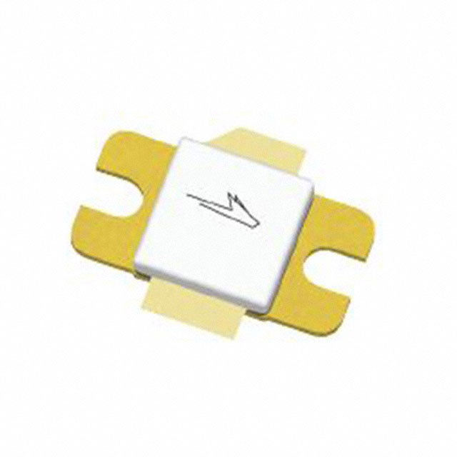
PTVA120251EA
Thermally-Enhanced High Power RF LDMOS FET
25 W, 50 V, 500 – 1400 MHz
Description
The PTVA120251EA LDMOS FET is designed for use in power amplifier applications in the 500 MHz to 1400 MHz frequency band. Features
include high gain and a thermally-enhanced package with bolt-down
flange. Manufactured with Wolfspeed's advanced LDMOS process, this
device provides excellent thermal performance and superior reliability.
Features
Power Sweep, Pulsed RF
VDD = 50 V, IDQ = 20 mA, TCASE = 25°C
300 µs pulse width, 12% duty cycle
• Unmatched input and output
• High gain and efficiency
70
• Integrated ESD protection
55
60
• Low thermal resistance
50
50
Efficiency
Output Power
45
40
1200 MHz
1300 MHz
1400 MHz
1200 MHz
1300 Mhz
1400 MHz
40
35
30
30
22
26
30
• Excellent ruggedness
• Pb-free and RoHS-compliant
• Capable of withstanding a 10:1 load mismatch
(all phase angles) at POUT = 25 W, under CW
conditions
20
a120251ea-v2-gr1a```
18
• ESD HBM Class 2, per ANSI/ESDA/JEDEC JS-001
Drain Efficiency (%)
60
Output Power (dBm)
PTVA120251EA
Package H-36265-2
34
10
Input Power (dBm)
RF Characteristics
Typical RF Performance (not subject to production test, verified by design/characterization in Wolfspeed test fixture)
VDD = 50 V, IDQ = 0.02 A, Input signal (tr = 5 ns, tf = 6.5 ns), 300 µs pulse width, 12% duty cycle, class AB test
Mode of operation
P1dB
P3dB
ƒ
IRL
Gain
Eff
POUT
Gain
Eff
(MHz)
(dB)
(dB)
(%)
(W)
(dB)
(%)
(W)
dB @ 30 W
(ns)
(ns)
Pulsed RF 1200
12
16.4
52
31
14.4
56
41
0.27
6
8
Pulsed RF 1300
11
16.0
56
32
14.0
59
40
0.20
6
8
Pulsed RF 1400
14
15.8
53
34
13.8
56
38
0.24
6
8
POUT Pdroop(pulse)
tr
tf
All published data at TCASE = 25°C unless otherwise indicated
ESD: Electrostatic discharge sensitive device—observe handling precautions!
Rev. 05, 2018-06-19
4600 Silicon Drive | Durham, NC 27703 | www.wolfspeed.com
�PTVA120251EA
2
RF Characteristics
Pulsed RF Performance (tested in Wolfspeed test fixture)
VDD = 50 V, IDQ = 0.02 A, POUT = 25 W, ƒ1 = 1200 MHz, ƒ2 = 1300 MHz, ƒ3 = 1400 M Hz, 300 µs pulse width, 10% duty cycle
Characteristic
Symbol
Min
Typ
Max
Unit
Gain
Gps
17
18
—
dB
Drain Efficiency
hD
47
54
—
%
Return Loss
IRL
—
–13
–9
dB
DC Characteristics
Characteristic
Conditions
Symbol
Min
Typ
Max
Unit
Drain-Source Breakdown Voltage
VGS = 0 V, IDS = 10 mA
V(BR)DSS
105
—
—
V
Drain Leakage Current
VDS = 50 V, VGS = 0 V
IDSS
—
—
1.0
µA
VDS = 105 V, VGS = 0 V
IDSS
—
—
10.0
µA
On-State Resistance
VGS = 10 V, VDS = 0.1 V
RDS(on)
—
1.4
—
W
Operating Gate Voltage
VDS = 50 V, IDQ = 150 mA
VGS
3
3.35
4
V
Gate Leakage Current
VGS = 10 V, VDS = 0 V
IGSS
—
—
1.0
µA
Maximum Ratings
Parameter
Symbol
Value
Unit
Drain-Source Voltage
VDSS
105
V
Gate-Source Voltage
VGS
–6 to +12
V
Operating Voltage
VDD
0 to +55
V
Junction Temperature
TJ
225
°C
Storage Temperature Range
TSTG
–65 to +150
°C
Thermal Resistance (TCASE = 70°C, VDD = 50 V, 25 W CW)
RqJC
3.7
°C/W
Ordering Information
Type and Version
Order Code
Package and Description
Shipping
PTVA120251EA V2 R0
PTVA120251EA-V2-R0
H-36265-2, bolt-down
Tape & Reel, 50 pcs
PTVA120251EA V2 R250
PTVA120251EA-V2-R250
H-36265-2, bolt-down
Tape & Reel, 250 pcs
Rev. 05, 2018-06-19
4600 Silicon Drive | Durham, NC 27703 | www.wolfspeed.com
�3
PTVA120251EA
Typical RF Performance (data taken in production test fixture)
Power Sweep, Pulsed RF
Power Sweep, Pulsed RF
VDD = 50 V, IDQ = 20 mA, TCASE = 25°C
300 µs pulse width, 12% duty cycle
VDD = 50 V, IDQ = 20 mA, POUT = 25 W
300 µs pulse width, 12% duty cycle
19
19
70
17
16
15
1200 MHz
1300 MHz
1400 MHz
22
26
50
17
30
16
1150
34
Power Sweep, Pulsed RF
Pulsed CW Performance
at Selected VDD
IDQ = 20 mA, ƒ = 1300 MHz
300 µs, 12% duty cycle
-12
0.24
-14
0.20
-16
-18
Power Droop
0.12
-20
-22
1450
a120251ea-v2-gr1d
1250
1350
Frequency (MHz)
80
30 V
35 V
40 V
45 V
50 V
17
Gain (dB)
Input Return Loss
Input Return Loss (dB)
Power Droop (dB)
19
-10
0.28
Rev. 05, 2018-06-19
1350
Frequency (MHz)
0.32
0.08
1150
40
1450
a120251ea-v2-gr1c
1250
Input Power (dBm)
VDD = 50 V, IDQ = 20 mA at P1dB
300 µs pulse width, 12% duty cycle
0.16
55
Gain
45
a120251ea-v2-gr1b
18
60
60
15
40
13
20
Efficiency (%)
14
13
Efficiency
18
Drain Efficiency (%)
65
Gain (dB)
Gain (dB)
18
Gain
Efficiency
11
a120251ea-v2-gr6
28
32
36
40
44
48
0
Output Power (dBm)
4600 Silicon Drive | Durham, NC 27703 | www.wolfspeed.com
�PTVA120251EA
4
Typical RF Performance (cont.)
Power Sweep, Pulsed RF
Power Sweep, Pulsed RF
VDD = 50 V, IDQ = 20 mA
2 ms pulse width, 10% duty cycle
VDD = 50 V, IDQ = 20 mA
2 ms pulse width, 10% duty cycle
POUT (dBm)
50
1200 MHz
40
1300 MHz
35
1200 MHz
30
1400 MHz
1300 Mhz
1400 MHz
a120251ea-v2-gr2a
18
22
26
60
18
50
Output Power
45
19
30
34
40
30
20
Gain (dB)
Efficiency
55
70
Drain Efficiency (%)
60
Gain
17
16
15
1200 MHz
1300 MHz
14
13
10
1400 MHz
a120251ea-v2-gr2b
18
20
22
24
26
28
30
32
34
Input Power (dBm)
Input Power (dBm)
Power Sweep, Pulsed RF
Power Sweep, Pulsed RF
VDD = 50 V, IDQ = 20 mA at P1dB
2 ms pulse width, 10% duty cycle
VDD = 50 V, IDQ = 20 mA, POUT = 25 W
2 ms pulse width, 10% duty cycle
19
70
-10
0.26
Efficiency
17
50
Gain
0.22
0.20
0.18
-14
0.16
0.14
-16
Input Return Loss
0.12
16
1150
1250
1300
1350
Frequency (MHz)
Rev. 05, 2018-06-19
40
1450
a120251ea-v2-gr2c
1200
1400
-12
Power Droop
IRL (dB)
60
Power Droop (dB)
18
Drain Efficiency (%)
Gain (dB)
0.24
0.10
1150
-18
1450
a120251ea-v2-gr2d
1200
1250
1300
1350
1400
Frequency (MHz)
4600 Silicon Drive | Durham, NC 27703 | www.wolfspeed.com
�5
PTVA120251EA
Typical RF Performance (cont.)
Power Sweep, Pulsed RF
Power Sweep, Pulsed RF
VDD = 50 V, IDQ = 20 mA
128 µs pulse width, 10% duty cycle
VDD = 50 V, IDQ = 20 mA
128 µs pulse width, 10% duty cycle
60
70
19
60
18
50
Output Power
45
40
1200 MHz
1300 MHz
1400 MHz
1200 MHz
1300 Mhz
1400 MHz
40
35
30
30
a120251ea-gr3a
18
22
26
30
34
Gain
17
16
15
20
14
10
13
1200 MHz
1300 MHz
1400 MHz
a120251ea-gr3b
18
20
Power In (dBm)
24
26
28
30
32
34
Power In (dBm)
Power Sweep, Pulsed RF
Power Sweep, Pulsed RF
VDD = 50 V, IDQ = 20 mA at P1dB
128 µs pulse width, 10% duty cycle
VDD = 50 V, IDQ = 20 mA, POUT = 25 W
128 µs pulse width, 10% duty cycle
19
70
-10
0.18
Power Droop
60
Efficiency
17
50
Gain
Power Droop (dB)
18
Drain Efficiency (%)
0.16
Gain (dB)
22
-12
0.14
0.12
-14
0.10
0.08
0.06
IRL (dB)
50
Gain (dB)
55
Drain Efficiency (%)
Output Power (dBm)
Efficiency
-16
Input Return Loss
0.04
16
1150
1350
Frequency (MHz)
Rev. 05, 2018-06-19
40
1450
a120251ea-gr3c
1250
0.02
1150
-18
1450
a120251ea-gr3d
1250
1350
Frequency (MHz)
4600 Silicon Drive | Durham, NC 27703 | www.wolfspeed.com
�PTVA120251EA
6
Typical RF Performance (cont.)
Power Sweep, Pulsed RF
Power Sweep, Pulsed RF
VDD = 50 V, IDQ = 20 mA
16 ms pulse width, 50% duty cycle
VDD = 50 V, IDQ = 20 mA, TCASE = 25°C
16 ms pulse width, 50% duty cycle
50
60
18
50
45
40
40
30
1200 MHz
1300 MHz
1400 MHz
35
30
19
a120251ea-v2-gr4a
18
20
22
24
26
28
30
32
17
Gain
16
15
14
20
13
10
12
1200 MHz
1300 MHz
1400 MHz
a120251ea-v2-gr4b
18
20
Input Power (dBm)
22
24
Power Sweep, Pulsed RF
32
34
Power Sweep, Pulsed RF
0.32
70
-4
Efficiency
17
50
Gain
Power Droop (dB)
60
18
Drain Efficiency (%)
0.28
Gain (dB)
30
VDD = 50 V, IDQ = 20 mA at P1dB
16 ms pulse width, 50% duty cycle
19
-6
Input Return Loss
0.24
-8
0.20
-10
Power Droop
0.16
-12
0.12
40
1450
a120251ea-v2-gr4c
1250
1350
Frequency (MHz)
Rev. 05, 2018-06-19
28
Input Power (dBm)
VDD = 50 V, IDQ = 20 mA, POUT = 25 W
16 ms pulse width, 50% duty cycle
16
1150
26
IRL (dB)
55
70
Gain (dB)
Output Power
Efficiency
Drain Efficiency (%)
Output Power (dBm)
60
-14
0.08
1150
-16
1450
a120251ea-v2-gr4d
1250
1350
Frequency (MHz)
4600 Silicon Drive | Durham, NC 27703 | www.wolfspeed.com
�7
PTVA120251EA
Typical RF Performance (tested with LTN/PTVA120251EA E4 test fixture, 960 MHz – 1215 MHz)
CW Performance
Small Signal CW Performance
Gain (dB)
20.0
5
65
17.5
0
15.0
-5
12.5
-10
10.0
-15
17
55
16
45
15
35
14
13
12
25
1200 MHz
1300 MHz
1400 MHz
a120251ea-v2-gr5
32
34
36
38
40
42
44
46
Power Gain (dB)
Gain
Efficiency
18
75
Efficiency (%)
19
15
7.5
5
5.0
Gain
-20
IRL
Input Return Loss (dB)
VDD = 50 V, IDQ = 80 mA
VDD = 50 V, IDQ = 20 mA
-25
1700
a120251ea-v2-gr7
900
1100
1300
1500
Frequency (MHz)
Output Power (dBm)
See next page for further performance characterization
Rev. 05, 2018-06-19
4600 Silicon Drive | Durham, NC 27703 | www.wolfspeed.com
�PTVA120251EA
8
Typical RF Performance (cont.) (tested with LTN/PTVA120251EA E4 test fixture, 960 MHz – 1215 MHz)
Power Sweep, Pulsed RF
Power Sweep, Pulsed RF
IDQ = 20 mA, VDD = 50 V, TCASE = 25°C,
128 µs pulse width, 10% duty cycle
IDQ = 20 mA, VDD = 50 V, TCASE = 25°C,
128 µs pulse width, 10% duty cycle
65
20
Drain Efficiency (%)
18
Gain (dB)
Gain
16
14
960 MHz
1030 MHz
1090 MHz
1150 MHz
1215 MHz
12
10
55
45
Efficiency
35
25
15
5
a120251e1a_g4-1
0
5
10
15
20
25
30
35
960 MHz
1030 MHz
1090 MHz
1150 MHz
1215 MHz
40
a120251e1a_g4-2
0
5
10
Output Power (W)
25
30
35
40
CW Performance
CW Performance
VDD = 50 V, IDQ = 20 mA
60
Drain Efficiency (%)
20
18
Gain (dB)
20
Output Power (W)
VDD = 50 V, IDQ = 20 mA
Gain
16
14
960 MHz
1030 MHz
1090 MHz
1150 MHz
1215 MHz
12
10
15
5
10
15
20
25
Output Power (W)
Rev. 05, 2018-06-19
30
40
35
Efficiency
30
960 MHz
1030 MHz
1090 MHz
1150 MHz
1215 MHz
20
10
0
a120251e1a_gCW-3
0
50
a120251e1a_gCW-4
0
5
10
15
20
25
30
35
Output Power (W)
4600 Silicon Drive | Durham, NC 27703 | www.wolfspeed.com
�9
PTVA120251EA
Typical RF Performance (cont.) (tested with LTN/PTVA120251EA E3 test fixture, 470 MHz – 860 MHz)
Test Conditions: DVB-T 8 MHz unclipped input signal, output PAR measured at 0.01% point of CCDF curve, ACPR measured
over 200 KHz BW at 4.1 MHz offset from carrier center frequency.
DVB-T Performace
ACPR vs Frequency at
various Average POUT
DVB-T Performace
Efficiency vs Frequency at
various Average POUT
VDD = 40 V, IDQ = 140 MA
VDD = 40 V, IDQ = 140 mA
30
-30
-32
Drain Efficiency (%)
ACPR (dB)
25
POUT = 36 dBm
-34
-36
POUT = 30 dBm
-38
-40
POUT = 32 dBm
POUT = 34 dBm
-42
-44
POUT = 34 dBm
15
10
POUT = 32 dBm
POUT = 30 dBm
5
-46
-48
POUT = 36 dBm
20
a120251ea_40V_g1
450
550
650
750
850
Frequency (MHz)
0
a120251ea_40V_g2
450
550
650
750
850
Frequency (MHz)
DVB-T Performace
PAR @ 0.01% CCDF vs Frequency
at various Average POUT
VDD = 40 V, IDQ = 140 mA
PAR @ 0.01% CCDF (dB)
11
POUT = 30 dBm
10
POUT = 32 dBm
9
POUT = 34 dBm
8
POUT = 36 dBm
7
6
a120251ea_40V_g3
450
550
650
750
850
Frequency (MHz)
Rev. 05, 2018-06-19
4600 Silicon Drive | Durham, NC 27703 | www.wolfspeed.com
�PTVA120251EA
10
Broadband Circuit Impedance
D
Z Source
Z Load
G
S
Z Source W
Z Load W
Freq
[MHz]
R
jX
R
jX
1200
4.31
–0.22
6.46
7.63
1300
5.06
–0.79
6.29
7.27
1400
4.94
–1.96
6.14
8.72
See next page for reference circuit information
Rev. 05, 2018-06-19
4600 Silicon Drive | Durham, NC 27703 | www.wolfspeed.com
�11
PTVA120251EA
Reference Circuits
DUT
Test Fixture Part No.
PCB
Frequency (MHz)
PTVA120251EA
LTN/PTVA120251EA V2 *
Rogers 6006, 0.635 mm [0.025”] thick,
2 oz. copper, εr = 6.15
1200 – 1400
PTVA120251EA
LTN/PTVA120251EA E2 †
Rogers 3010, 0.635 mm [0.025”] thick,
2 oz. copper, εr = 10.2
1200 – 1400
PTVA120251EA
LTN/PTVA120251EA E3 †
Rogers 4350B, 0.762mm [.030"] thick,
2 oz. copper, εr = 3.48
470 – 860
PTVA120251EA
LTN/PTVA120251EA E4 †
Rogers 3010, 0.635 mm [0.025”] thick,
2 oz. copper, εr = 10.2
960 – 1215
* See pages 11 – 12 for assembly information. Find Gerber files for this reference circuit on the Wolfspeed Web site at
www.wolfspeed.com/RF
† Gerber files for this reference circuit are available on request.
C803
C802
S2
R101
+
S1
VDD
R803
C801
R801
C203
S3
R804
R805
C201
C102
R802
C202
C104
RF_IN
R201
R102
C103
R103
C204
PTVA120251_IN
RF_OUT
C205
C101
RO6006, 025 (62)
PTVA120251_OUT
RO6006, 025 (63)
a 1 20 25 1 e a_ c d_ 0 6- 1 9- 2 01 8
Assembly diagram for reference circuit LTN/PTVA120251EA V2, 1200 MHz to 1400 MHz (not to scale)
Rev. 05, 2018-06-19
4600 Silicon Drive | Durham, NC 27703 | www.wolfspeed.com
�PTVA120251EA
12
Reference Circuit (cont.)
Components Information
Component
Description
Manufacturer
P/N
C101, C102
Capacitor, 56 pF
ATC
ATC100B560JW500XB
C103
Capacitor, 1 µF
TDK Corporation
C4532X7R2A105M230KA
C104
Capacitor, 10 µF
TDK Corporation
C5750X5R1H106K230KA
C801, C802,
C803
Capacitor, 1000 pF
Kemet
C1812C560KHGACTU
R101
Resistor, 5.6 ohms
Panasonic Electronic Components
ERJ-8RQJ5R6V
R102
Resistor, 0 ohms
Panasonic Electronic Components
ERJ-8RQJ5R6V
R103, R801
Resistor, 10 ohms
Panasonic – ECG
ERJ-3GEYJ100V
R802, R805
Resistor, 2K ohms
Panasonic Electronic Components
ERJ-8GEYJ202V
R803
Chip resistor, 1.3K ohms
Panasonic Electronic Components
ERJ-3GEYJ132V
R804
Chip resistor, 1.2K ohms
Panasonic Electronic Components
ERJ-3GEYJ122V
S1
Potentiometer 2K ohms
Bourns Inc.
3224W-1-202E
S2
Voltage regulator
Fairchild Semiconductor
LM7805
S3
Transistor
Fairchild Semiconductor
BCP56
C201
Capacitor, 10 µF
TDK Corporation
C5750X5R1H106K230KA
C202
Capacitor, 1 µF
TDK Corporation
C4532X7R2A105M230KA
C203
Capacitor, 100 µF
Cornell Dubilier Electronics
SK101M100ST
C204, C205
Capacitor, 56 pF
ATC
ATC100B560JW500XB
C206
Capacitor, 6800 µF
Panasonic Electronic Components
ECO-S2AP682EA
R101
Resistor, 5.6 ohms
Panasonic Electronic Components
ERJ-8GEYJ5R6V
Input
Output
Rev. 05, 2018-06-19
4600 Silicon Drive | Durham, NC 27703 | www.wolfspeed.com
�13
PTVA120251EA
Package Outline Specifications
Package H-36265-2
45° X 2.03
[.080]
6. ALL FOUR
CORNERS
2X 7.11
[.280]
2.66±.51
[.105±.020]
D
S
FLANGE
9.78
[.385]
3.05
[.120]
LID
10.16±.25
[.400±.010]
C
L
G
2X R1.52
[R.060]
C
L
4X R0.63
[R.025] MAX
SPH 1.57
[.062]
15.49±.51
[.610±.020]
4X R1.52
[R.060]
15.23
[.600]
10.16±.25
[.400±.010]
3.61±.38
[.142±.015]
h - 3 6 2 6 5 - 2 _ p o _ 0 9 - 0 8 - 2 0 1 1
1.02
[.040]
20.31
[.800]
6.
Diagram Notes—unless otherwise specified:
1. Interpret dimensions and tolerances per ASME Y14.5M-1994.
2. Primary dimensions are mm. Alternate dimensions are inches.
3. All tolerances ±0.127 [0.005] unless specified otherwise.
4. Pins: D – drain; G – gate; S – source
5. Lead thickness: 0.10 + 0.051/–0.025 mm [0.004 + 0.002/–0.001 inch].
6. Exposed metal plane on top and bottom of ceramic insulator.
7. Gold plating thickness: 1.14 ± 0.38 micron [45 ± 15 microinch].
Rev. 05, 2018-06-19
4600 Silicon Drive | Durham, NC 27703 | www.wolfspeed.com
�PTVA120251EA
14
Revision History
Revision
Date
Data Sheet Type
Page
Subjects (major changes since last revision)
01
2012-06-04
Preliminary
All
First release of Data Sheet for pre-production product
02
2012-10-29
Preliminary
6
Add DVB-T performance graphs
03
2013-03-25
Production
All
1–2
3–8
9 – 11
Data Sheet reflects released product specifications and performance
Update tables with current data
Add further graphs
Add load pull performance and reference circuit information
04
2014-10-03
Production
11 – 12
1, 3 – 7
New circuit design.
Characterization in new circuit.
04.1
2015-06-15
Production
2
Updated max of IRL in pulsed RF performance table
04.2
2016-04-19
Production
2
Updated ordering information
04.3
2017-02-07
Production
2
Updated operating voltage and junction temperature
05
2018-06-19
Production
All
Converted to Wolfspeed Data Sheet
For more information, please contact:
4600 Silicon Drive
Durham, North Carolina, USA 27703
www.wolfspeed.com/RF
Sales Contact
RFSales@wolfspeed.com
RF Product Marketing Contact
RFMarketing@wolfspeed.com
919.407.7816
Notes
Disclaimer
Specifications are subject to change without notice. Cree, Inc. believes the information contained within this data sheet
to be accurate and reliable. However, no responsibility is assumed by Cree for any infringement of patents or other rights
of third parties which may result from its use. No license is granted by implication or otherwise under any patent or patent rights of Cree. Cree makes no warranty, representation or guarantee regarding the suitability of its products for any
particular purpose. “Typical” parameters are the average values expected by Cree in large quantities and are provided for
information purposes only. These values can and do vary in different applications and actual performance can vary over
time. All operating parameters should be validated by customer’s technical experts for each application. Cree products
are not designed, intended or authorized for use as components in applications intended for surgical implant into the
body or to support or sustain life, in applications in which the failure of the Cree product could result in personal injury or
death or in applications for planning, construction, maintenance or direct operation of a nuclear facility.
Copyright © 2018 Cree, Inc. All rights reserved. The information in this document is subject to change without notice. Wolfspeed™ and the Wolfspeed logo are trademarks of Cree, Inc.
Rev. 05, 2018-06-19
www.wolfspeed.com
�