Spec. No.:
Date:
RMC-1K-17N1011
2017. 11. 28
/1
Data sheet
Title:
FIXED
RECTANGULAR TYPE
Style:
RMC10,16,20,32,35
Automotive Grade
AEC-Q200 qualified
RoHS COMPLIANCE ITEM
Halogen and Antimony Free
Note: ・Stock conditions
Temperature: +5°C ∼ +35°C
Relative humidity: 25% ∼ 75%
The period of guarantee: Within 2 year from shipmen t by the company.
Solderability shall be satisfied.
・Product specification contained in this data sheet
are subject to change at any time without notice
・If you have any questions or a Purchasing Specification for any quality
Agreement is necessary, please contact our sales staff.
Hokkaido Research Center
Approval by: T. Sannomiya
Drawing by: M. Shibuya
�Drawing No:
RMC−1K−17N1011
/1
Title:
RMC10,16,20,32,35 Automotive Grade
Page:
1. Scope
1.1 This specification covers the detail requirements for fixed thick film chip resistors
35.
1/10
10, 16, 20,32,
1.2 Applicable documents
JIS C 5201−1: 2011, IEC60115−1: 2008, AEC-Q200 Rev.D
1.3 For Automotive Grade
- AEC-Q200 qualified (Grade 0)
- Managed and manufactured under the exclusive manufacturing process for automotive.
2. Classification
Type designation shall be the following form.
(Example)
1)
RMC
32
−
1
2
3
Style
2)
RMC
32
1
2
Style
1 Fixed
2 Rated dissipation and / or dimension
3 Temperature coefficient of resistance
123
4
J
5
JP
4
TP
6
Style
K
−(Dash)
4 Rated resistance
123
1000
JP
TP
6
±100×10−6/ °C
Standard
E24 Series, 3 digit, Ex. 123--> 12kΩ,
E96 Series, 4 digit, Ex. 1000-->100Ω
1022--> 10.2kΩ
Chip jumper
5 Tolerance on rated resistance
B
±0.1%
D
±0.5%
F
±1%
G
±2%
J
±5%
6 Packaging form 1. Scope
B
Bulk (loose package)
TH
Paper taping
TP
TE
Embossed taping
Product specification contained in this data sheet are subject to change at any time without notice.
If you have any questions or a Purchasing Specification for any quality agreement is necessary, please contact our sales staff.
Issue: KAMAYA ELECTRIC CO., LTD. Research & Development Department HOKKAIDO Research center Last update: 2017.11.28
�Drawing No:
RMC−1K−17N1011
/1
Title:
RMC10,16,20,32,35 Automotive Grade
Page:
2/10
3. Rating
3.1 The ratings shall be in accordance with Table−1.
Table−1(1)
Style
RMC10
Rated
dissipation
(W)
Temperature coefficient of
resistance (10−6 / °C)
K
±100
10∼1M
Standard
K
±200
±100
±200
+500∼−200
±200
±200
+500∼−200
1.02M∼3.3M
10∼1M
1.02M∼10M
1∼9.76
10∼10M
10∼10M
1∼9.1
±100
10∼3.3M
±100
+500∼−200
±200
+500∼−200
±200
+500∼−200
10∼10M
1∼9.76
10∼10M
1.0∼9.1
10∼22M
1.0∼9.1
±100
10∼2.2M
Standard
±200
2.21M∼3.3M
K
±100
±200
+500∼−200
±200
+500∼−200
±200
+500∼−200
10∼2.2M
2.21M∼10M
1.0∼9.76
10∼10M
1.0∼9.1
10∼22M
1.0∼9.1
K
±100
10∼1M
Standard
±200
+500∼−200
±200
+500∼−200
±200
+500∼−200
1.02M∼10M
1.0∼9.76
10∼10M
1.0∼9.1
10∼24M
1.0∼9.1
±100
10∼1M
±200
+500∼−200
1.02M∼10M
1.0∼9.76
10∼1M
10∼22M
1.0∼9.1
0.1
Standard
K
RMC16
0.1
Standard
K
RMC20
Rated resistance
range (Ω)
0.125
Standard
Preferred
number series
for resistors
E24, 96
0.25
K
G(±2%)
E24
E24, 96
0.5
Standard
±200
+500∼−200
J(±5%)
B(±0.1%)
D(±0.5%)
F(±1%)
G(±2%)
E24
J(±5%)
E24,96
B(±0.1%)
D(±0.5%)
D(±0.5%)
F(±1%)
G(±2%)
E24
J(±5%)
B(±0.1%)
D(±0.5%)
F(±1%)
F(±1%)
G(±2%)
E24
J(±5%)
E24,96
RMC35
B(±0.1%)
D(±0.5%)
D(±0.5%)
F(±1%)
E24,96
RMC32
Tolerance on
rated resistance
B(±0.1%)
D(±0.5%)
F(±1%)
F(±1%)
G(±2%)
E24
J(±5%)
Product specification contained in this data sheet are subject to change at any time without notice.
If you have any questions or a Purchasing Specification for any quality agreement is necessary, please contact our sales staff.
Issue: KAMAYA ELECTRIC CO., LTD. Research & Development Department HOKKAIDO Research center Last update: 2017.11.28
�Drawing No:
RMC−1K−17N1011
/1
Title:
RMC10,16,20,32,35 Automotive Grade
Style
Limiting element
voltage (V)
Table−1(2)
Isolation voltage
(V)
Page:
3/10
Category temperature
range (°C)
RMC10
50
100
RMC16
RMC20
150
−55∼+155
RMC32
500
200
RMC35
Note. Rated current of chip jumper: RMC10: 1(A), RMC16, 20, 32, 35: 2(A)
Note. Resistance value of chip jumper: 50 mΩ max.
3.2 Climatic category
55/155/56
3.3 Stability class
2%
Lower category temperature
Upper category temperature
Duration of the damp heat, steady state test
− 55 °C
+155 °C
56days
Limits for change of resistance:
−for long−term tests
±(2%+0.1Ω) Chip jumper: 50 mΩ max.
−for short−term tests
±(0.5%+0.05Ω) Chip jumper: 50 mΩ max.
3.4 Derating
The derated values of dissipation (or current rating in case of chip jumper) at temperature in excess of 70 °C shall be as
indicated by the following curve.
100
Percentage of the
rated dis sipation
(Current) (%)
0
−55
Area of recommended
operation
70
155
Ambient temperature (° C)
Figure−1 Derating curve
3.5 Rated voltage
d. c. or a. c. r. m. s. voltage calculated from the square root of the product of the rated resistance and the rated dissipation.
E : Rated voltage (V)
E =
P · R
P : Rated dissipation (W)
R : Rated resistance (Ω)
Limiting element voltage can only be applied to resistors when the resistance value is equal to or higher than the critical
resistance value.
At high value of resistance, the rated voltage may not be applicable.
Product specification contained in this data sheet are subject to change at any time without notice.
If you have any questions or a Purchasing Specification for any quality agreement is necessary, please contact our sales staff.
Issue: KAMAYA ELECTRIC CO., LTD. Research & Development Department HOKKAIDO Research center Last update: 2017.11.28
�Drawing No:
RMC−1K−17N1011
/1
Title:
RMC10,16,20,32,35 Automotive Grade
Page:
4/10
4. Packaging form
The standard packaging form shall be in accordance with Table−2.
Table−2
Symbol
B
TH
TP
TE
Standard packaging
quantity / units
1,000 pcs.
10,000 pcs.
5,000 pcs.
4,000 pcs.
Packaging form
Bulk (loose package)
Paper taping
8mm width, 2mm pitches
Paper taping
8mm width, 4mm pitches
Embossed taping
8mm width, 4mm pitches
Application
RMC10,16,20,32,35
RMC10
RMC16, 20, 32
RMC35
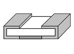
5. Dimensions
5.1 The resistor shall be of the design and physical dimensions in accordance with Figure−2 and Table−3.
z
W
z
L
c
d
d
H
c
Style
RMC10
RMC16
RMC20
RMC32
RMC35
L
1.0±0.05
1.6±0.1
2.0±0.1
3.1±0.1
3.1±0.15
W
0.5±0.05
+0.15
0.8−0.05
1.25±0.10
1.6±0.15
2.5±0.15
Figure−2
Table−3
H
0.35±0.05
0.45±0.10
0.55±0.10
0.55±0.10
0.55±0.15
Unit : mm
c
0.2±0.1
0.3±0.1
0.4±0.2
0.5±0.25
0.5±0.25
d
+0.05
0.25−0.10
0.3±0.1
0.4±0.2
0.5±0.25
0.5±0.25
z
--------0.05~0.3
0.05~0.3
5.2 Net weight (Reference)
Style
Net weight(mg)
RMC10
0.6
RMC16
2
RMC20
5
RMC32
9
RMC35
16
Product specification contained in this data sheet are subject to change at any time without notice.
If you have any questions or a Purchasing Specification for any quality agreement is necessary, please contact our sales staff.
Issue: KAMAYA ELECTRIC CO., LTD. Research & Development Department HOKKAIDO Research center Last update: 2017.11.28
�Drawing No:
RMC−1K−17N1011
/1
Title:
RMC10,16,20,32,35 Automotive Grade
Page:
5/10
6. Marking
The Rated resistance of RMC 10 should not be marked.
6.1 RMC20,32,35.
The nominal resistance shall be marked in 3 digits or 4 digits and marked on over coat side.
• E24 series: 3 digits, E96 series: 4 digits
In case of the resistance value that E96 overlaps with E24, It is marked by either.
Marking example
Contents
Application
123
2R2
2.2
5623
12R7
12×10 3 [Ω] → 12 [kΩ]
2. 2 [Ω]
2. 2 [Ω]
562×10 3 [Ω] → 562[kΩ]
12.7 [Ω]
RMC20,32,35
Less than 10Ω of RMC32,35
Less than 10Ω of RMC20
RMC20,32,35
RMC20,32,35
6.2 RMC16
The nominal resistance shall be marked in 3 digits and marked on over coat side.
No marking in the E96 series.
Marking example
Contents
Application
123
E24
12×10 3 [Ω] → 12 [kΩ]
E24
2R2
2. 2 [Ω]
2
No marking
E96
102×10 [Ω] → 10.2 [kΩ]
No marking
E96
332×10−1 [Ω] → 33.2 [Ω]
6.3 Marking example of Jumper Chip
Marking example
Contents
or 000
JP
000
Application
RMC16
RMC20,32
RMC35
Product specification contained in this data sheet are subject to change at any time without notice.
If you have any questions or a Purchasing Specification for any quality agreement is necessary, please contact our sales staff.
Issue: KAMAYA ELECTRIC CO., LTD. Research & Development Department HOKKAIDO Research center Last update: 2017.11.28
�Drawing No:
RMC−1K−17N1011
/1
Title:
RMC10,16,20,32,35 Automotive Grade
Page:
6/10
7. Performance
7.1 The standard condition for tests shall be in accordance with Sub−clause 4.2, JIS C 5201−1: 1998.
7.2 The performance shall be satisfied in Table−4.
Table−4(1)
Test items
Condition of test
Performance requirements
No.
1
High temperature exposure
MIL-STD-202 Method 108
Resistor: ∆R/R: Within ±(2%+0.1Ω)
AEC Q200 - No.3
Ambient temperature:155±2°C,
Chip jumper: 50mΩ max.
Condition: Without load,
No visible damage
Duration: 1000 +480 h
Interval measurements: 250 h and 500 h
2
Temperature cycling
JESD22 Method JA-104
Resistor: ∆R/R: Within ±(1%+0.05Ω)
AEC Q200 - No.4
Temperature: -55±3°C / 125±2°C,
Chip jumper: 50mΩ max.
Dwell time: 30min maximum at each temp.
No visible damage
Transition time: 1 min. max.
Number of cycles: 1000 cycles.
Interval measurements: 250 cy and 500 cy
3
Bias humidity
MIL-STD-202 Method 103
Resistor: ∆R/R: Within ±(2%+0.1Ω)
AEC Q200 – No.7
Condition: 85°C & 85% R.H.
Chip jumper: 50mΩ max.
Test power: 10% of rated power shall be No visible damage
applied for continuously.
Duration: 1,000 +480 h
Interval measurements: 250 h and 500 h
4
Operational life
MIL-STD-202 Method 108
Resistor: ∆R/R: Within ±(2%+0.1Ω)
AEC Q200 – No.8
Ambient temperature: 125±2ºC
Chip jumper: 50mΩ max.
The applied voltage shall be the voltage to be No visible damage
calculated at 35% of rated dissipation or the
limiting element voltage whichever is the
smaller.
Condition: The voltage shall be applied for
continuously.
+48
Duration: 1000
h
0
Interval measurements: 250 h and 500 h
5
Dimensions
JESD22 Method JB-100
As in Table−3
AEC Q200 – No.10
6
Resistance to Solvents
MIL-STD-202 Method 215
Resistor: ∆R/R: Within ±(1%+0.05Ω)
AEC Q200 – No.12
Solvent: 2−propanol at 25℃
Chip jumper: 50mΩ max.
Immersion time: 3 min
No visible damage
Brush: 10 times brushing
Immersion and brush cycle: 3cycle
7
Mechanical Shock
MIL-STD-202 Method 213
Resistor: ∆R/R: Within ±(0.5%+0.05Ω)
AEC Q200 – No.13
Waveform: half sine,
Chip jumper: 50mΩ max.
Peak value100G,
No visible damage
Normal duration 6ms
Condition: XX'YY'ZZ', 10times each
Product specification contained in this data sheet are subject to change at any time without notice.
If you have any questions or a Purchasing Specification for any quality agreement is necessary, please contact our sales staff.
Issue: KAMAYA ELECTRIC CO., LTD. Research & Development Department HOKKAIDO Research center Last update: 2017.11.28
�Drawing No:
RMC−1K−17N1011
/1
Title:
RMC10,16,20,32,35 Automotive Grade
No
8
Test items
Vibration
AEC Q200 – No.14
9
Resistance to soldering heat
AEC Q200 - No.15
10
ESD test
AEC Q200 – No.17
11
Solderability
AEC Q200 – No.18
12
Electrical Characterization
AEC Q200 - No.19
13
Bending strength
AEC Q200 – No.21
14
Adhesion
AEC Q200 – No.22
Page:
7/10
Table−4(2)
Condition of test
MIL-STD-202 Method 204
Performance requirements
Resistor: ∆R/R: Within ±(0.5%+0.05Ω)
Peak acceleration and Sweep time: 5 g's for 20 Chip jumper: 50mΩ max.
min , Frequency 10Hz to 2000Hz,
No visible damage
Condition: 12 cycles each of 3 orientations
MIL-STD-202 Method 210
Resistor: ∆R/R: Within ±(0.5%+0.05Ω)
Solder bath temp: 260±5ºC
Chip jumper: 50mΩ max.
Immersed time: 10±1s
No visible damage
AEC-Q200-002
Resistor: ∆R/R: Within ±(5%+0.1Ω)
Human body model, 2 Kohm, 150 pF,
No visible damage
Test voltage: RMC16,1/10.1/8,1/4 2000V
RMC10 800V
J-STD-002
The surface of terminal immersed shall
a) Bake the sample for 155 ºC dwell time 4h / be min. of 95% covered with a new
solder dipping 235ºC/ 5s.
coating of solder.
Solder: Sn96.5-Ag3-Cu0.5
b) Category 3, Solder dipping 215ºC/ 5s.
Solder: Sn63Pb37
c) Category 3, Solder dipping 260ºC/ 7s.
1. D.C. Resistance
1. The resistance value shall
2. Temperature Coefficient of Resistance
correspond with the rated resistance
-55 °C / +20°C
taking into account the specified
+20 °C / +155°C
tolerance.
2. As in Table−1
AEC-Q200-005
Resistor: ∆R/R: Within ±(0.5%+0.05Ω)
Bending value2mm
Chip jumper: 50mΩ max.
Holding time: 60sec.
No visible damage
AEC-Q200-006
Resistor: ∆R/R: Within ±(0.5%+0.05Ω)
Pressurizing force:
Chip jumper: 50mΩ max.
RMC20,32,35 17.7N
No visible damage
RMC10,16 10N
Test time: 60±1s.
Product specification contained in this data sheet are subject to change at any time without notice.
If you have any questions or a Purchasing Specification for any quality agreement is necessary, please contact our sales staff.
Issue: KAMAYA ELECTRIC CO., LTD. Research & Development Department HOKKAIDO Research center Last update: 2017.11.28
�Drawing No:
RMC−1K−17N1011
/1
Title:
RMC10,16,20,32,35 Automotive Grade
Page:
8/10
9. Taping
9.1 Applicable documents JIS C 0806−3: 2014, EIAJ ET−7200C: 2010
9.2 Taping dimensions
9.2.1 Paper taping (8mm width, 2mm pitches)
Taping dimensions shall be in accordance with Figure−3 and Table−5.
4±0.1
t1
Sprocket hole
φ1.5
Unit: mm
0 .1
+0
0
1.75±0.1
B
8±0.2
A
t2
2±0.05
Carrier cavity
3.5±0.05
Direction of unreeling
Style
RMC10
A
0.65+0.05
−0.10
Figure−3
Table−5
B
1.15 −+0.05
0.10
t1
0.4 ± 0.05
Unit: mm
t2
0.5max.
9.2.2 Paper taping (8mm width, 4mm pitches)
Taping dimensions shall be in accordance with Figure−4 and Table−6.
Unit: mm
4±0.1
t
1
φ1.5
Sprocket hole
+0.1
0
2±0.05
1.75±0.1
B
8±0.2
A
t
Carrier cavity
2
4±0.1
3.5±0.05
Direction of unreeling
Style
RMC16
RMC20
RMC32
Figure−4
Table−6
A
B
1.15±0.15
1.9±0.2
1.65±0.15
2.5±0.2
2.00±0.15
3.6±0.2
t1
0.6±0.1
Unit: mm
t2
0.8max.
0.8±0.1
1.0max.
Product specification contained in this data sheet are subject to change at any time without notice.
If you have any questions or a Purchasing Specification for any quality agreement is necessary, please contact our sales staff.
Issue: KAMAYA ELECTRIC CO., LTD. Research & Development Department HOKKAIDO Research center Last update: 2017.11.28
�Drawing No:
RMC−1K−17N1011
/1
Title:
RMC10,16,20,32,35 Automotive Grade
Page:
9/10
9.2.3 Embossed taping dimensions shall be in accordance with Figure−5 and Table−7.
Unit: mm
0.3 max.
2±0.05
Sprocket hole
φ1.5+0.1
0
1.75±0.1
4±0.1
W
B
E
A
Carrier cavity
t1
Style
RMC35
Direction of unreeling
4±0.1
Figure−5
Table−7
B
W
3.5±0.2
8.0±0.3
A
2.85±0.20
E
3.5±0.05
Unit: mm
t1
1.0±0.2
1). The cover tapes shall not cover the sprocket holes.
2). Tapes in adjacent layers shall not stick together in the packing.
3). Components shall not stick to the carrier tape or to the cover tape.
4). Pitch tolerance over any 10 pitches ±0.2mm.
5). The peel strength of the top cover tape shall be with in 0.1N to 0.5N on the test method as shown in the
following RMC10, 16, 20, 32: Figure−6, RMC35: Figure−7.
6). When the tape is bent with the minimum radius for 25 mm, the tape shall not be damaged and the components shall maintain
their position and orientation in the tape.
7). In no case shall there be two or more consecutive components missing.
The maximum number of missing components shall be one or 0.1%, whichever is greater.
8). The resistors shall be faced to upward at the over coating side in the carrier cavity.
Top cover tape
Carrier tape
Peel−off
( About 300mm/ min)
165°to180°
Direction of unreeling
Figure−6
Top cover tape
Carrier tape
165°to180°
Peel−off
(About 300mm/ min)
Direction of unreeling
Figure−7
Product specification contained in this data sheet are subject to change at any time without notice.
If you have any questions or a Purchasing Specification for any quality agreement is necessary, please contact our sales staff.
Issue: KAMAYA ELECTRIC CO., LTD. Research & Development Department HOKKAIDO Research center Last update: 2017.11.28
�Drawing No:
RMC−1K−17N1011
/1
Title:
RMC10,16,20,32,35 Automotive Grade
Page:
10/10
9.3 Reel dimension
Reel dimensions shall be in accordance with the following Figure−8 and Table−8.
Plastic reel (Based on EIAJ ET−7200C)
Unit: mm
0
+1
φ60
0
φ13±0.2
2±0.5
φ180 −1.5
Marking A
φ21±0.8
Marking B
A
B
Figure−8
Table−8
A
Unit: mm
B
Note
Injection
molding
11.4±1.0
RMC 10, 16, 20, 32, 35
9 +1.0
0
13±1.0
Vacuum forming
Note: Marking label shall be marked on a place of Marking A or two place of marking A and B.
Style
9.4 Leader and trailer tape.
(Example)
400mm min.
100mm min.
160mm min.
End
Start
Trailer
Leader
Direction of unreeling
Figure−9
10. Marking on package
The label of a minimum package shall be legibly marked with follows.
10.1 Marking A
(1) Classification
(Style, Temperature coefficient of resistance, Rated resistance, Tolerance on rated resistance, Packaging form)
(2) Quantity (3) Lot number (4) Manufacturer’s name or trade mark
10.2 Marking B (KAMAYA Control label)
(5) Others
Product specification contained in this data sheet are subject to change at any time without notice.
If you have any questions or a Purchasing Specification for any quality agreement is necessary, please contact our sales staff.
Issue: KAMAYA ELECTRIC CO., LTD. Research & Development Department HOKKAIDO Research center Last update: 2017.11.28
�