Additional Resources:
Product Page
|
3D Model
|
PCB Footprint
date
07/12/2021
page
1 of 6
SERIES: PEM2-D │ DESCRIPTION: DC-DC CONVERTER
FEATURES
•
•
•
•
•
•
•
•
•
•
2 W isolated output
smaller package
single/dual unregulated output
3,000 Vdc isolation
short circuit protection
extended temperature range (-40~105°C)
antistatic protection up to 8kV
high efficiency at light load
efficiency up to 85%
EN 62368-1
MODEL
input
voltage
PEM2-S5-S5-D1
output
voltage
output
current
output
power
ripple
and noise2
efficiency
typ
(Vdc)
range
(Vdc)
(Vdc)
min
(mA)
max
(mA)
max
(W)
typ
(mVp-p)
typ
(%)
5
4.5~5.5
5
40
400
2
75
80
1
PEM2-S5-S12-D
5
4.5~5.5
12
17
167
2
75
84
PEM2-S5-S15-D1
5
4.5~5.5
15
13
133
2
75
84
PEM2-S5-D5-D
5
4.5~5.5
±5
±20
±200
2
75
80
PEM2-S5-D12-D1
5
4.5~5.5
±12
±8
±83
2
75
84
1
PEM2-S5-D15-D
5
4.5~5.5
±15
±7
±67
2
75
84
PEM2-S12-S5-D1
12
10.8~13.2
5
40
400
2
75
80
PEM2-S12-S15-D
12
10.8~13.2
15
13
133
2
75
84
PEM2-S12-D15-D1
12
10.8~13.2
±15
±7
±67
2
75
85
PEM2-S15-D15-D
15
13.5~16.5
±15
±7
±67
2
75
84
PEM2-S24-S5-D1
24
21.6~26.4
5
40
400
2
75
80
PEM2-S24-S9-D
24
21.6~26.4
9
22
222
2
75
85
PEM2-S24-S15-D1
24
21.6~26.4
15
13
133
2
75
84
1
PEM2-S24-D12-D
24
21.6~26.4
±12
±8
±83
2
75
83
PEM2-S24-D15-D1
24
21.6~26.4
±15
±7
±67
2
75
84
1
1
Notes:
1. UL approved
2. Ripple and noise are measured at 20 MHz BW by “parallel cable” method with 1 μF ceramic and 10 μF electrolytic capacitors on the output.
PART NUMBER KEY
PEM2 - SXX - XXX -D
Base Number
Input Voltage
Output
S = single
D = dual
cui.com
Output Voltage
Packaging Style
DIP
�Additional Resources:
Product Page
|
3D Model
|
PCB Footprint
CUI Inc │ SERIES: PEM2-D │ DESCRIPTION: DC-DC CONVERTER
date 07/12/2021 │ page 2 of 6
INPUT
parameter
conditions/description
min
typ
max
units
operating input voltage
5 Vdc input models
12 Vdc input models
15 Vdc input models
24 Vdc input models
4.5
10.8
13.5
21.6
5
12
15
24
5.5
13.2
16.5
26.4
Vdc
Vdc
Vdc
Vdc
surge voltage
for maximum of 1 second
5 Vdc input models
12 Vdc input models
15 Vdc input models
24 Vdc input models
-0.7
-0.7
-0.7
-0.7
9
18
21
30
Vdc
Vdc
Vdc
Vdc
filter
capacitance filter
max
units
±1.2
%
OUTPUT
parameter
conditions/description
min
line regulation
for Vin change of 1%
load regulation
measured from 10%~100% load
5 Vdc output models
9 Vdc output models
12 Vdc output models
15 Vdc output models
voltage accuracy
see tolerance envelope curve
switching frequency
100% load, nominal input voltage
temperature coefficient
at 100% load
typ
10
9
8
7
%
%
%
%
100
kHz
±0.03
%/°C
max
units
1
s
max
units
PROTECTIONS
parameter
conditions/description
min
typ
short circuit protection1
Note:
1. The supply voltage must be discontinued at the end of the short circuit duration
SAFETY AND COMPLIANCE
parameter
conditions/description
isolation voltage
input to output for 1 minute at 1 mA max.
3,000
Vdc
isolation resistance
input to output at 500 Vdc
1,000
MΩ
safety approvals2
certified to 62368-1: EN
certified to 60950-1: UL
conducted emissions
CISPR22/EN55022, class B, external circuit required
radiated emissions
CISPR22/EN55022, class B, external circuit required
ESD
IEC/EN61000-4-2, class B, contact ± 8kV for single outputs
IEC/EN61000-4-2, class B, contact ± 6kV for dual outputs
MTBF
as per MIL-HDBK-217F @ 25°C
RoHS
2011/65/EU
Note:
min
typ
3,500,000
hours
2. See specific models noted on page 1
ENVIRONMENTAL
parameter
conditions/description
min
max
units
operating temperature
see derating curve
-40
105
°C
-55
125
°C
storage temperature
storage humidity
non-condensing
temperature rise
Ta=25°C
typ
95
25
cui.com
%
°C
�Additional Resources:
Product Page
|
3D Model
|
PCB Footprint
CUI Inc │ SERIES: PEM2-D │ DESCRIPTION: DC-DC CONVERTER
date 07/12/2021 │ page 3 of 6
SOLDERABILITY
parameter
conditions/description
max
units
hand soldering
1.5 mm from case for 10 seconds
min
typ
300
°C
wave soldering
see wave soldering profile
260
°C
max
units
MECHANICAL
parameter
conditions/description
dimensions
20.32 x 10.16 x 8.2 (0.800 x 0.400 x 0.323 inch)
min
case material
epoxy resin (UL94-V0)
weight
typ
mm
2.8
g
MECHANICAL DRAWING
units: mm[inch]
tolerance: ±0.25[±0.010]
pin section tolerance: ±0.10[±0.004]
PIN CONNECTIONS
PIN
Single Output
Dual Output
1
GND
GND
7
NC
NC
8
+Vo
+Vo
9
NO PIN
0V
10
0V
-Vo
14
Vin
Vin
Front View
Bottom View
cui.com
Top View
PCB Layout
�Additional Resources:
Product Page
|
3D Model
|
PCB Footprint
CUI Inc │ SERIES: PEM2-D │ DESCRIPTION: DC-DC CONVERTER
date 07/12/2021 │ page 4 of 6
DERATING CURVES
EMC RECOMMENDED CIRCUIT
Figure 1
Table 1
Recommended external circuit components
Vin
(Vdc)
C1,C2
CY
LDM
5
4.7μF/50V
-
6.8μH
12
4.7μF/50V
-
6.8μH
15
4.7μF/50V
-
6.8μH
4.7μF/50V
1nF/3KV
6.8μH
24
Note:
cui.com
1. See Table 2 for Cout values.
�Additional Resources:
Product Page
|
3D Model
|
PCB Footprint
CUI Inc │ SERIES: PEM2-D │ DESCRIPTION: DC-DC CONVERTER
date 07/12/2021 │ page 5 of 6
APPLICATION NOTES
1. Output load requirement
To ensure this module can operate efficiently and reliably, the minimum output load may not be less than 10% of the full load during
operation. If the actual output power is low, connect a resistor at the output end in parallel to increase the load.
2. Overload Protection
Under normal operating conditions, the output circuit of this product has no protection against overload. The simplest method to add
this is to add a circuit breaker to the circuit.
3. Recommended circuit
If you want to further decrease the input/output ripple, you can increase the capacitance accordingly or choose capacitors with low
ESR(see Figure 2 & Table 2). However, the capacitance of the output filter capacitor must be appropriate. If the capacitance is too
high, a startup problem might arise. For every channel of the output, to ensure safe and reliable operation, the maximum capacitance
must be less than the maximum capacitive load (see Table 3).
Figure 2
Single output
Dual output
Table 2
Vin
(Vdc)
Cin
(µF)
Single Vo
(Vdc)
Cout
(µF)
Table 3
Dual Vo
(Vdc)
Cout
(µF)
Single Vout
(Vdc)
Max. Capacitive Load
(μF)
Dual Vout
(Vdc)
Max. Capacitive Load1
(μF)
5
4.7
5
10
±5
4.7
5
220
5
100
12
2.2
9
4.7
±12
1
9
220
--
--
15
2.2
12
2.2
±15
0.47
12
220
12
100
24
1
15
1
--
--
15
220
15
100
Note:
Notes:
It’s not recommended to connect any external capacitors in
applications with less than 0.5 watt output.
1.
2.
3.
4.
Note:
1. For each output.
Operation under minimum load will not damage the converter; however, they may not meet all specifications listed.
Max. capacitive load tested at input voltage range and full load.
It is recommended to use either ceramic capacitors or electrolytic capacitors on the input and the output. Using tantalum capacitors may increase the risk of failure.
All specifications measured at: Ta=25°C, humidity
很抱歉,暂时无法提供与“PEM2-S5-D5-D”相匹配的价格&库存,您可以联系我们找货
免费人工找货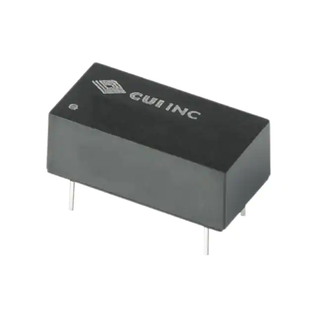


 工商网监
湘ICP备2023018690号
工商网监
湘ICP备2023018690号
