High Performance, Low
Power HDMI/DVI Transmitter
AD9387NK
General
Low power HDMI/DVI transmitter ideal for portable
applications
Compatible with HDMI v.1.3, DVI v.1.0, and HDCP 1.3
Single 1.8 V power supply
Video/audio inputs accept logic levels from 1.8 V to 3.3 V
Digital video
80 MHz operation supports all HDTV resolutions from
480i to 1080i
Programmable 2-way color space converter
Supports RGB, YCbCr, and DDR
Supports ITU656-based embedded syncs
Automatic input video format timing detection (CEA-861D)
Digital audio
Supports standard S/PDIF for stereo LPCM or compressed
audio up to 192 kHz
8-channel, uncompressed LPCM I2S audio up to 192 kHz
Special features for easy system design
On-chip MPU with I2C master to perform HDCP operations
and EDID reading operations
5 V tolerant I2C and HPD I/Os, no extra device needed
No audio master clock needed for supporting S/PDIF
and I2S
On-chip MPU reports HDMI events through interrupts and
registers
APPLICATIONS
Digital video cameras
Digital still cameras
Personal media players
Cellular handsets
DVD players and recorders
Digital set-top boxes
A/V receivers
HDMI repeater/splitter
GENERAL DESCRIPTION
FUNCTIONAL BLOCK DIAGRAM
SCL SDA
MCL MDA
INT
I2 C
SLAVE
HDCP
CORE
HDCP AND EDID
MICROCONTROLLER
I2C
MASTER
REGISTER
CONFIGURATION
LOGIC
CLK
VSYNC
HSYNC
DE
VIDEO
DATA
CAPTURE
I2S[3:0]
LRCLK
SCLK
DDCSDA
Tx0[1:0]
S/PDIF
MCLK
DDCSCL
SYNC
ADJUSTMENT
AND
GENERATION
COLOR
SPACE
CONVERSION
D[23:0]
HPD
Tx1[1:0]
HDMI Tx
CORE
AUDIO
DATA
CAPTURE
Tx2[1:0]
TxC[1:0]
AD9387NK
06880-001
FEATURES
Figure 1.
The AD9387NK supports both S/PDIF and 8-channel I2S audio.
Its high fidelity, 8-channel I2S can transmit either stereo or 7.1
surround audio at 192 kHz. The S/PDIF can carry stereo linear
pulse-code modulation (LPCM) audio or compressed audio,
including Dolby® Digital and DTS®.
The AD9387NK helps reduce system design complexity and cost
by incorporating such features as an internal microprocessor
for high-bandwidth digital content protection (HDCP) operations, an I2C® master for extended display identification data
(EDID) reading, a single 1.8 V power supply, and 5 V tolerance
on the I2C and hot plug detect pins. For additional information
and resources, see the Applications Information section.
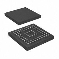
Fabricated in an advanced CMOS process, the AD9387NK
is available in a space saving, 76-ball CSP_BGA. The package is
RoHS compliant and is specified from −25°C to +90°C
operation.
The AD9387NK is an 80 MHz, high definition multimedia
interface (HDMI™) v.1.3 transmitter. It supports HDTV formats
up to 720p and 1080i and computer graphic resolutions up to
XGA (1024 × 768 @ 75 Hz). With the inclusion of HDCP, the
AD9387NK allows the secure transmission of protected content,
as specified by the HDCP 1.3 protocol.
Rev. 0
Information furnished by Analog Devices is believed to be accurate and reliable. However, no
responsibility is assumed by Analog Devices for its use, nor for any infringements of patents or other
rights of third parties that may result from its use. Specifications subject to change without notice. No
license is granted by implication or otherwise under any patent or patent rights of Analog Devices.
Trademarks and registered trademarks are the property of their respective owners.
One Technology Way, P.O. Box 9106, Norwood, MA 02062-9106, U.S.A.
Tel: 781.329.4700
www.analog.com
Fax: 781.461.3113
©2007 Analog Devices, Inc. All rights reserved.
�AD9387NK
TABLE OF CONTENTS
Features .............................................................................................. 1
Explanation of Test Levels ............................................................4
Applications ....................................................................................... 1
ESD Caution...................................................................................4
General Description ......................................................................... 1
Applications Information .................................................................5
Functional Block Diagram .............................................................. 1
Design Resources ..........................................................................5
Revision History ............................................................................... 2
Document Conventions ...............................................................5
Specifications..................................................................................... 3
Outline Dimensions ..........................................................................6
Absolute Maximum Ratings............................................................ 4
Ordering Guide .............................................................................6
REVISION HISTORY
10/07—Revision 0: Initial Version
Rev. 0 | Page 2 of 8
�AD9387NK
SPECIFICATIONS
Table 1. AD9387NKBBCZ-80/AD9387NKBBCZRL-80
Parameter
DIGITAL INPUTS
Input Voltage, High (VIH)
Input Voltage, Low (VIL)
Input Capacitance
THERMAL CHARACTERISTICS
Thermal Resistance
Junction-to-Case BGA (θJC)
Junction-to-Ambient (θJA)
Ambient Temperature
DC SPECIFICATIONS
Input Leakage Current (IIL)
AC SPECIFICATIONS
CLK Frequency
TMDS Output CLK Duty Cycle
Input Data Setup Time
Input Data Hold Time
TMDS Differential Swing
VSYNC and HSYNC Delay from DE Falling Edge
VSYNC and HSYNC Delay to DE Rising Edge
Differential Output Swing
Low-to-High Transition Time
High-to-Low Transition Time
AUDIO AC TIMING
Sample Rate
I2S Cycle Time
I2S Setup Time
I2S Hold Time
1
2
Conditions
I2S and S/PDIF
See the Explanation of Test Levels section.
UI = unit interval.
Rev. 0 | Page 3 of 8
Temp
Test Level 1
Min
Full
Full
25°C
VI
VI
VIII
1.4
−0.3
Full
V
V
V
−25
Full
VI
Full
Full
Full
Full
Max
Unit
3.5
+0.7
3
V
V
pF
+90
°C/W
°C/W
°C
−10
+10
μA
IV
IV
IV
IV
VI
IV
IV
13.5
48
1
0.7
900
80
52
MHz
%
ns
ns
mV
UI 2
UI2
25°C
25°C
VII
VII
75
75
Full
25°C
25°C
25°C
IV
IV
IV
IV
32
2
2
Typ
15.2
59
+25
1000
1
1
1100
175
175
ps
ps
192
1
kHz
UI2
ns
ns
�AD9387NK
ABSOLUTE MAXIMUM RATINGS
EXPLANATION OF TEST LEVELS
Table 2.
Parameter
Digital Inputs
Digital Output Current
Operating Temperature Range
Storage Temperature Range
Maximum Junction Temperature
Maximum Case Temperature
Rating
−0.3 V to +5 V
20 mA
−40°C to +100°C
−65°C to +150°C
150°C
150°C
Stresses above those listed under Absolute Maximum Ratings
may cause permanent damage to the device. This is a stress
rating only; functional operation of the device at these or any
other conditions above those indicated in the operational
section of this specification is not implied. Exposure to absolute
maximum rating conditions for extended periods may affect
device reliability.
I.
100% production tested.
II.
100% production tested at 25°C and sample tested at
specified temperatures.
III.
Sample tested only.
IV.
Parameter is guaranteed by design and characterization
testing.
V.
Parameter is a typical value only.
VI.
100% production tested at 25°C; guaranteed by design
and characterization testing.
VII.
Limits defined by HDMI specification; guaranteed by
design and characterization testing.
VIII.
Guaranteed by design.
ESD CAUTION
Rev. 0 | Page 4 of 8
�AD9387NK
APPLICATIONS INFORMATION
DESIGN RESOURCES
DOCUMENT CONVENTIONS
The following resources, as well as evaluation kits,
reference design schematics, and other support
documentation, are available after signing an NDA
available from flatpanel_apps@analog.com. Users can
access a programming guide, a hardware user guide, a
software driver user guide, and software driver source
code after signing an NDA.
In this data sheet, data is represented using the conventions
described in Table 3.
Other references include the following:
0bNN
Table 3. Document Conventions
Data
Type
0xNN
EIA/CEA-861, a technical specifications document, describes
audio and video InfoFrames, as well as the E-EDID structure for
HDMI. It is available from the Consumer Electronics
Association (CEA).
NN
Bit
HDMI v.1.3, a defining document for HDMI v.1.3, and the
HDMI Compliance Test Specification v.1.3 are available from
HDMI Licensing, LLC.
HDCP Specification v.1.3, the defining technical specifications
document for the HDCP v.1.3, is available from Digital Content
Protection, LLC.
Rev. 0 | Page 5 of 8
Format
Hexadecimal (Base 16) numbers are represented using
the C language notation, preceded by 0x.
Binary (Base 2) numbers are represented using the C
language notation, preceded by 0b.
Decimal (Base 10) numbers are represented using no
additional prefixes or suffixes.
Bits are numbered in little endian format; that is, the
least significant bit of a byte or word is referred to as Bit 0.
�AD9387NK
OUTLINE DIMENSIONS
A1 CORNER
INDEX AREA
6.10
6.00 SQ
5.90
10 9
8
7 6
5
4
3 2 1
A
B
BALL A1
PAD CORNER
TOP VIEW
C
4.50
BSC SQ
D
E
0.50
BSC
F
G
H
J
K
DETAIL A
BOTTOM VIEW
0.75
REF
*1.40 MAX
DETAIL A
0.65 MIN
0.15 MIN
COPLANARITY
0.08 MAX
*COMPLIANT TO JEDEC STANDARDS MO-225
WITH THE EXCEPTION TO PACKAGE HEIGHT.
010807-A
0.35 SEATING
0.30 PLANE
0.25
BALL DIAMETER
Figure 2. 76-Ball Chip Scale Package Ball Grid Array [CSP_BGA]
6 mm × 6 mm × 1.4 mm
(BC-76-1)
Dimensions shown in millimeters
ORDERING GUIDE
Model
AD9387NKBBCZ-80 1
AD9387NKBBCZRL-801
AD9387NK/PCBZ1
1
Temperature Range
−25°C to +90°C
−25°C to +90°C
Package Description
76-Ball Chip Scale Package Ball Grid Array [CSP_BGA]
76-Ball Chip Scale Package Ball Grid Array [CSP_BGA]
Evaluation Board
Z = RoHS Compliant Part.
Rev. 0 | Page 6 of 8
Package Option
BC-76-1
BC-76-1
�AD9387NK
NOTES
Rev. 0 | Page 7 of 8
�AD9387NK
NOTES
Purchase of licensed I2C components of Analog Devices or one of its sublicensed Associated Companies conveys a license for the purchaser under the Philips I2C Patent
Rights to use these components in an I2C system, provided that the system conforms to the I2C Standard Specification as defined by Philips.
©2007 Analog Devices, Inc. All rights reserved. Trademarks and
registered trademarks are the property of their respective owners.
D06880-0-10/07(0)
Rev. 0 | Page 8 of 8
�


 工商网监
湘ICP备2023018690号
工商网监
湘ICP备2023018690号
