National Semiconductor
November 29, 2007
Rev – 1.1/CS
RoHS Compliant
Evaluation Board User's Guide
ADC122S706 Dual 12-Bit, 500 kSPS to 1 MSPS,
Simultaneous Sampling A/D Converter
�Table of Contents
1.0 Introduction ............................................................................................................................3
2.0 Board Assembly .....................................................................................................................4
3.0 Quick Start .............................................................................................................................4
3.1 Stand-Alone Mode ....................................................................................................4
3.2 Computer Mode ........................................................................................................5
4.0 Functional Description............................................................................................................6
4.1 Analog Input Signal ...................................................................................................6
4.2 ADC Reference Circuitry...........................................................................................6
4.3 SPI Interface .............................................................................................................6
4.4 Power Supply Connections .......................................................................................7
5.0 Software Operation and Settings ...........................................................................................7
6.0 Evaluation Board Specifications ............................................................................................9
7.0 Summary Tables of Test Points, Jumpers, and Connectors .................................................9
8.0 Hardware Schematic..............................................................................................................10
9.0 Board Layouts ........................................................................................................................11
10.0 Evaluation Board Bill of Materials ........................................................................................12
2
http://www.national.com
�1.0 Introduction
The ADC122S706EB/RoHS Design Kit (consisting
of the ADC122S706 Evaluation Board and this
User's Guide) is designed to ease evaluation and
design-in of the National Semiconductor
ADC122S706 12-bit Analog-to-Digital Converter.
This ADC has two analog input channels that are
sampled simultaneously and can operate at
speeds up to 1 MSPS. The converter’s digital
outputs are available on single or dual data ouput
pins.
The evaluation board can be used in either of two
modes. In Stand Alone, suitable test equipment
such as a logic analyzer can be used with the
board
to
evaluate
the
ADC122S706’s
performance.
In the Computer mode, data capture and
evaluation is simplified by connecting the
evaluation board to National Semiconductor's
Data Capture Board (order number WAVEVSN
BRD 4.1 or higher) which connects to a personal
computer through a USB port and runs
WaveVision 4 software revision 4.4 or higher.
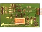
JP1: VREF
The latest version of the WaveVision 4 software
should be downloaded from the web at
http://www.national.com/adc.
Note: WaveVision software version 4.4 or higher
is required to evaluate this part with the WV4
Evaluation System.
The WaveVision 4 software operates under
Microsoft Windows. The signal at the analog
input is digitized, captured, and displayed on a PC
monitor in the time and frequency domains.
The software will perform an FFT on the captured
data upon command. This FFT plot shows the
dynamic performance in the form of SNR, SINAD,
THD, SFDR, and ENOB. A software histogram of
the captured data is also available.
The signals at analog input J1 are digitized by U2,
the ADC122S706. The ADC122S706 either uses
a crystal oscillator (Y1) which is provided on this
board or an externally supplied clock at TP9.
JP2: VIO
J1: INPUT
JP7: CLK
JP5: DUAL
JP6: VA
Figure 1 Component and Test Point Locations
3
http://www.national.com
�2.0 Board Assembly
The ADC122S706EB evaluation board comes
fully assembled and ready for use. The provided
shorting jumpers are in their recommended
locations and suit the needs of most users. The
evaluation board also includes a crystal oscillator
(Y1).
Refer to the Bill of Materials for a
description of components, to Figure 1 for major
component placement, and to Figure 10 for the
evaluation board schematic.
While the board has been populated in a manner
that is most advantageous for typical usage, the
board can be customized by adding components
to meet the user’s specific needs. The board
comes ready to use with a DC coupled input
signal (Figure 2). However, by adding capacitors
C6, C7, C10, C11 (value 1µF), adding DC bias
resistors R1, R2, R3, R4, R5, R9, R12, R14 (value
4.99kΩ), and removing R6, R11, R13, R17 (value
20Ω), the board can be used with an AC coupled
input signal (Figure 3).
Figure 2: DC Coupled Input Configuration
Figure 3: AC Coupled Input Configuration
The board was tested with several different
capacitor
configurations,
and
the
best
performance was found to occur when capacitors
C33, C34, C35, C36 were not populated and only
differential capacitors C9 and C8 were left in
place. If your analog input signal has a great deal
of common-mode noise, the user can populate
C33, C34, C35, C36 with 470pF capacitors.
4
3.0 Quick Start
The ADC122S706EB evaluation board may be
used in the Stand-Alone mode to capture data
with a logic analyzer or third party equipment, or it
may be used in the Computer Mode with a
WaveVision 4 Data Capture Board, referenced
throughout the remainder of this document as
WV4. In both cases, the data may be analyzed
with the WaveVision 4 software.
3.1 Stand Alone Mode
Refer to Figure 1 for locations of test points and
major components.
1. Remove the jumper from JP7 and the
oscillator Y1 from its socket. The SPI interface
signals (CSB and SCLK) may be driven
directly at J2 or with wires soldered to VIA1
and VIA2 (step 7). DOUTA and DOUTB may
also be monitored at J2 or with wires at VIA3
and VIA4. Please note that the schematic
and PCB silkscreen refers to DOUTA and
DOUTB as DOUT1 and DOUT2. Frequently,
a Logic Analyzer with a built-in pattern
generator is used to drive CSB and SCLK
while monitoring the data outputs.
It is
necessary to remove Y1 because the
presence of a second clock source could add
noise to the conversion process.
2. Connect a clean analog (not switching) +5.0V
power source with a 300mA current limit to
the external power connector TP6. Ground
TP7.
3. Place a shorting jumper across pins 1 & 2 of
JP6 and turn on the power supply.
4. To analyze the performance of channel A,
connect a differential signal across pins 1 & 3
of J1 (pin 2 is ground). Please note the
evaluation board is assembled for a DCcoupled input source. To analyze channel B,
connect your signal across pins 4 & 6 of J1
(pin 5 is ground). If the source has a 50 ohm
output impedance, install a 51 ohm resistor at
R7 or R15, depending on which channel you
are using (match the source impedance with
resistors R7 or R15). To accurately evaluate
the performance of the ADC122S706, the
source must be better than 90dB THD.
5. Select the 2.5V voltage reference as VREF by
placing a shorting jumper across pins 2 & 3
of JP1.
6. If it is desirable to provide an external
reference voltage, the jumper must be
removed from JP1 and TP1 (VREF) may be
http://www.national.com
�driven directly. Refer to the datasheet for
acceptable common mode voltage ranges for
specific reference voltages.
7. Apply the signals to control the SPI interface
at J2 or VIA1 to VIA4. See the evaluation
board schematic (Figure 10) or the J2 header
pin out (Figure 5) for more details.
3.2 Computer Mode
Refer to Figure 1 for locations of test points and
major components.
1. Run the WaveVision 4 program, version 4.4 or
higher is required to interface to the WV4
board. While the program is loading, continue
below.
2. Connect a USB cable between the WV4
board and the PC running the WaveVision 4
software.
3. Connect the J2 header on the ADC122S706
evaluation board to the J7 WV4 serial
connector on the WV4 board. Refer to Figure
4 for the serial connection and Figure 5 for the
J2 header pin out.
Figure 4: WV4 to ADC122S706 Connection
5
Figure 5: J2 (WV4S) Header Pin Out
4. Connect a clean analog (not switching) +5.0V
power source with a 300mA current limit to
power connector J1 on the WV4 board.
Ground the GND connector and turn on the
power.
5. Connect a clean analog (not switching) +5.0V
power source with a 300mA current limit to
power connector TP6 on the ADC board.
Ground pin TP7 and turn on the power. Place
a shorting jumper between pins 1 & 2 of JP6
to power the board. LED D1 should be ON.
Note: The evaluation board can also be
powered directly from the WV4 board by
placing a shorting jumper between pins 2 & 3
and removing the external supply.
6. Place a 16 MHz crystal oscillator into the
socket at Y1 and place a shorting jumper
between pins 1 & 2 of JP7. Alternatively,
connect a signal generator to TP9 (CLK_IN)
and place a shorting jumper between pins 2
& 3 of JP7 to use an external clock.
7. Make
the
following
required
jumper
connections, see table 1 for more details:
• JP1 - pins 2 & 3
• JP2 - pins 1 & 2
• JP5 - pins 1 & 2
8. Perform step 4 of section 3.1 to drive the
analog inputs. For information on changing
the configuration of the analog input section,
read section 2.0 Board Assembly for details.
The board comes ready for a DC coupled
differential input signal.
9. Perform step 5 or 6 of section 3.1 to select the
reference voltage.
10. Refer to section 5.0 on Software Operation
and Settings to setup WaveVision 4.
http://www.national.com
�4.0 Functional Description
Table 1 describes the function of the various
jumpers on the ADC122S706 evaluation board.
The evaluation board schematic is shown in
Figure 10.
Pins 1 & 2
Pins 2 & 3
JP1
Select VA as VREF
Select +2.5V reg.
as VREF
JP2
Provides power to
the digital supply
input (required)
NA
JP5
The conversion of
Ch. A is outputted
on DOUTA and Ch.
B is outputted on
DOUTB
Conversion of Ch.
A and B outputted
on DOUTA, with A
being first, DOUTB
is high impedance
JP6
Select +5.0V
external supply
Select +5.0V from
J2 (WV4S)
JP7
Select on-board
clock OSC Y1
Select external
clock from TP9
Jumper
JP13
Enable OSC (not required)
Table 1: Jumper Configurations
4.1 Analog Input Signal
The input signal to be digitized can be a
differential voltage or a single-ended signal. A
differential signal can have a maximum value of
+/-VREF and is applied across pins 1 & 3 of J1 for
channel A and pins 4 & 6 of J1 for channel B.
Pins 2 and 5 are grounds. A single-ended signal
can have a maximum value of 2VREF and a
minimum value of 0V. The signal may be applied
to either the non-inverting or inverting input. The
opposing input pin must be driven by a maximum
voltage of VREF where VREF < VA / 2.
R7 and R15 are terminating resistors for the input
source. Since all sources do not have the same
output impedance, those resistors are not
populated. However, those resistors should be
added by the user with the appropriate value that
matches the source.
When using an AC coupled input signal, DC
biasing is required. DC biasing is available for
inputs applied to J1 but is currently not populated
on the board. Add 4.99 kΩ resistors to R3, R4,
R5, R9 to achieve a VA/2 DC bias on channel A
and add 4.99kΩ resistors to R1, R2, R12, R14 to
achieve a VA/2 DC bias on channel B. Proper DC
biasing will allow each input to swing the full range
(-VREF/2 to +VREF/2) where VREF < VA.
6
Dynamic input signals should be applied through
a bandpass filter to eliminate the noise and
harmonics commonly associated with signal
sources. To accurately evaluate the performance
of the ADC122S706, the source must be better
than -90dBc THD.
4.2 ADC Reference Circuitry
This evaluation board includes the option of
selecting a fixed 2.5V reference voltage, VA, or an
external voltage as the reference voltage. Select
the 2.5V reference as VREF by shorting pins 2 & 3
of JP1 or select VA as VREF by shorting pins 1 & 2
of JP1. If it is desirable to provide an external
reference voltage, the jumper must be removed
from JP1 and TP1 may be driven directly. The
recommended range for VREF is 1.0V to VA.
4.3 SPI Interface
4.3.1 ADC Clock (SCLK)
The clock frequency can range from 8MHz to
16MHz.
The 16MHz crystal-based oscillator
provided on the evaluation board is selected by
shorting pins 1 & 2 of JP7. It is best to remove
any external signal generator when using this
oscillator to reduce any unnecessary noise.
This board will also accept a clock signal from an
external source by connecting that source to TP9
(CLK_IN) and shorting pins 2 & 3 of JP7. The
input at TP9 is terminated by R22 (value 51Ω).
To reduce any unnecessary noise, it is best to
remove the oscillator at Y1 when using an
external clock source.
Regardless of the clock source selected by JP7,
the clock signal is designed to be routed off the
ADC122S706 evaluation board to the WV4 board.
This assumes computer mode operation of the
evaluation board. For applications utilizing the
evaluation board in manual mode, the clock is
applied directly at J2 or VIA2.
4.3.2 Digital Data Outputs (DOUTA & DOUTB)
The ADC122S706 enables system designers two
options for receiving converted data. Data can be
received from separate data output pins (DOUTA
and DOUTB) or from a single data output pin.
These options are controlled by the digital input
pin DUAL. In either case, the output format is 2’s
compliment.
The digital output configuration is controlled by
JP5. Placing a shorting jumper across pins 1 & 2
of JP5 will cause the conversion result of channel
A to be output on DOUTA and the conversion
http://www.national.com
�result of channel B to be output on DOUTB.
Placing a shorting jumper across pins 2 & 3 of
JP5 will cause the conversion result of channel A
and channel B to be outputted on the same line
(DOUTA) with channel A being output first;
DOUTB will be at a high impedance state.
The output on DOUTA can be monitored at VIA3
or pin 5 of J2, while the output on DOUTB can be
monitored at VIA4 or pin 7 of J2. Please note that
these pins are labeled DOUT1 and DOUT2
respectively on the schematic and PCB
silkscreen. In computer mode, the DOUTA and
DOUTB are monitored by the WV4 board and
WaveVision 4 software.
See the Evaluation
Board schematic (Figure 10) and Section 5.0 for
more details.
4.3.3 Chip Select Bar (CSB)
The CSB pin may be monitored at VIA1 or pin 1 of
J2. In computer mode, the CSB is provided by the
WV4 board. In manual mode, the CSB should be
driven directly at J2. The signal level for CSB
needs to be CMOS compatible. See the
ADC122S706 datasheet for logic threshold limits.
5.0 Software Operation and Settings
The WaveVision 4 software is included with the
WV4 board and the latest version can be
downloaded for free from National's web site at
http://www.national.com/adc.
WaveVision
software version 4.4 or later is required to
evaluate this device with the WaveVision system.
To install this software, follow the procedure in the
WV4 Board User's Guide. Once the software is
installed, run and set it up as follows:
1. Connect the WV4 board to the host computer
with a USB cable.
2. From the WaveVision main menu, go to
Settings and then Board Settings to open the
System Settings window (Figure 6) and select
the following:
• WaveVision 4.0 (USB)
• Number of Samples: 2K to 32K, as
desired
• Data Format: Two’s Complement
4.4 Power Supply Connections
In both the computer and manual modes, the
analog supply voltage (VA) can range between
+4.5V and +5.5V. Typical supply currents when
applying an external supply to TP6, 5P0V_REM
are as follows:
• for +4.5V - I = 10mA
• for +5.5V - I = 13mA
Note: A majority of this current is for powering
devices external to the ADC122S706. When
operating in the computer mode, the supply
voltage for VA can be applied externally or
supplied directly by the WV4 board through J2.
The external supply voltage is selected by placing
a shorting jumper across pins 1 & 2 of JP6 and
applying a +5.0V power source with a 300mA
current limit to TP6 and grounding TP7. To use
the supply directly from the WV4 board, place a
shorting jumper across pins 2 & 3 of JP6. For the
best performance, use an external supply. The
+3.3V required to power the EEPROM is obtained
through J2 from the WV4 board. LED D2 on the
evaluation board will be lit red indicating the
EEPROM is powered.
Figure 6: System Settings window
3. Apply power as specified in Section 4.4, click
on the "Test" button and await the firmware
to download.
4. Click on the "Accept" button to close the
System Settings window.
When operating in manual mode, always use an
external supply. Apply a +5.0V power source with
a current limit of 300mA to TP6 and ground TP7.
Place a shorting jumper across pins 1 & 2 of JP6.
7
http://www.national.com
�5. Select the channel to collect data from, either
channel A, B, or A & B (see Figure 7).
6. Select DUAL data output mode or SINGLE
data output mode (see Figure 7).
To view an FFT of the data captured, click on the
‘FFT’ tab. This plot may be zoomed in on the data
plot. A display of dynamic performance
parameters in the form of SINAD, SNR, THD,
SFDR and ENOB will be displayed at the top right
hand corner of the FFT plot (Figure 9). Typical
values using a VREF = 2.5V and a Vin = 4.9 Vpp are:
•
•
•
•
•
SINAD: 72.099
SNR: 72.486
THD: -82.791
SFDR: 83.755
ENOB: 11.7
Figure 7: Channel Select
7. After the steps outlined in Section 3.2 are
completed, click on ‘Acquire’ then ‘Samples’
from the Main Menu (you can also press the
F1 shortcut key). If a dialog box opens, select
‘Discard’ or press the Escape (Esc) key to
start collecting new samples.
WaveVision main menu will display an output plot.
Make sure there is no clipping of data samples.
Click on the software histogram tab and ensure
data does not exceed the limit of the device. The
samples may be further analyzed by clicking on
the magnifying glass icon, then clicking and
dragging across a specific area of the plot for
better data inspection (Figure 8).
See the
WaveVision 4 Board User's Guide for more
details.
Figure 9: FFT
Acquired data may be saved to a file. Plots may
also be exported as graphics. See the Data
Capture Board User's Guide for details.
Figure 8: Software Histogram
8
http://www.national.com
�6.0 Evaluation Board Specifications
Board Size:
Power Requirements:
Clock Frequency Range:
Differential Analog Input:
3.1" x 1.95" (7.9 cm x 5 cm)
Min: +4.5V,
Max: +5.5V,
10mA
13mA
8 MHz to 16 MHz
+/- VREF
7.0 Test Points, Connectors, and Jumpers
Test Points on the ADC122S706 Evaluation Board
TP1: VREF
VREF test point. Located at the top middle of the board.
TP2: VIO
Vi/o test point. Locate at the center of the board.
TP3: AGND
Ground. Located at the top middle of the board.
TP4: AGND
Ground. Located at the center of the board.
TP5: AGND
Ground. Located at the middle left area of the board.
TP6: 5P0_REM
5.0V remote test point. Located at the lower left corner of the board.
TP7: AGND
Ground. Located at the lower left corner of the board.
TP8: 3P3V
3.3V test point. Located at the middle right area of the board.
TP9: CLK_IN
Input Clock Signal. Located at the bottom right of the board.
TP10: AGND
Ground. Located at the bottom right of the board.
Connectors on the ADC122S706 Evaluation Board
J1: A-VIN and B-VIN
6 pin male header: Differential input for A and B.
J2: WV4S
14 pin dual row right angle male header: Connects to WV4 board.
Selection Jumpers on the ADC122S706 Evaluation Board (Refer to table 1 in Section 4.0 for configuration details)
9
JP1: VREF SELECT
Selects reference source for VREF.
JP2: VA=VIO
Provides power to the digital power supply input.
JP5: DUAL SELECT
Selects either to output A and B on different outputs channels, or the same.
JP6: VA SELECT
Selects VA (externally or from the WV4 board).
JP7: CLK SELECT
Selects clock source (on-board oscillator or external source).
http://www.national.com
�J1
1
2
3
4
5
6
HEADER 6
A-VIN
B-VIN
R7
NS
R15
NS
R6
C6
C7
R11
20
NS
NS
20
20
NS
NS
R13 20
C10
C11
R17
B-VBIAS
R2
NS
R1
NS
VA_T
R4
NS
R5
NS
NS
A-VBIAS
R3
NS
R9
NS
R12 NS
R14
VA_T
1
2
C34
C33
NS
NS
NS
3
C35
C8
VIN
VREF
+ C5
0.1uF
C4
10uF
C12
10uF
VA_T
470pF
1
C9
VA_T
470pF
4
5
U1 LM4132-2.5
NC
GND
EN
VA
RED LED
D1
NS
510
C36
C1
10uF
R16
TP6
5P0V_REMOTE
5P0V_REM
AGND
TP7
AGND 1
NS
R20
VA_T
51
VREF
AGND
TP1
VREF
VA_T
1
TP3
AGND
AIN-
AIN+
VREF
Vi/o
DOUT1
DOUT2
SCLK
CSB
VA_T
1
TP4
AGND 1
+ C3
10uF
VIO=VA
JP2
C2
TP2
VIO
1
J2
WV4S
2
SCLK
VIA2
CSB_T
CSB
VIA1
0.1uF
CSB
10
CLKSEND_T
SDA_T
C17
0.1uF
WV4S
SCL_T
5P0V_T
4
6
12
8
CLKSEND_T 9
14
SCLK SCLK_T 3
DOUT1 DOUT1_T 5
11
DOUT2 DOUT1
3P3V
3P3V
TP8
R24
200
D2
3P3V_T
DOUT2 DOUT2_T 7
13
51
3P3V_T
51
10
9
8
JP5
DUAL SELECT
C14
0.1uF
Y1
OSC (THROUGH-HOLE)
1
5P0V_T
AGND
R8
VIA3
R10
VIA4
12
AGND
TP5
11
13
U2
ADC122S705-TSSOP14
14
GND
GND
BINBIN+
DUAL
JP7
CLK SELECT
OUT
OE
VA SELECTION
JP6
VA SELECTION
5P0V_T
DUAL
VA_T
VA
0.1uF
C13
7
6
5
4
3
2
1
VREF SELECT
JP1
VREF SELECTION
+
R18
NS
CLK SELECT
CLKSEND_T
R19
8
JP13
OSC ENABLE
3P3V
RED LED
SDA
3P3V_T
R22 51
CLK_IN
TP9
CLK_IN
GND
5
SCL
3P3V_T
4
A2
7
WP
8
VCC
3
C15
0
1
TP10
AGND 1
1
A1
2
1
2
3
U3
24C02
http://www.national.com
10
1
A0
6
1
1
2
1
1
14
VDD
GND
7
2
3
1
1
1
1
3
2
1
1
2
3
+
8.0 Hardware Schematic
Figure 10: ADC122S706 Evaluation Board Schematic
�9.0 Evaluation Board Layers
Figure 11: ADC122S706 Evaluation Board: All Layers with Silk Screen
Figure 12: ADC122S706 Evaluation Board: Top Layer
Figure 13: ADC122S706 Evaluation Board: Bottom Layer
11
http://www.national.com
�10.0 Evaluation Board Bill of Materials
Qty.
Reference
PCB Footprint
Source
Source Part #
Rating
Value
50V
0.1uF
4
C1,C3,C4,C12
5
C2,C5,C13,C14,C17
21
R1,R2,R3,R4,R5,R7,C6,
C7,R9,C10,C11,R12,
JP13,R14,R15,R19,R20
C33, C34,C35,C36
2
C8,C9
sm/c_0603
1
C15
sm/c_1206
2
D1,D2
sm/led_21
Digikey
516-1440-1-ND
RED LED
1
JP1
blkcon.100/vh/tm1sq/w.100/3
Digikey
S1011E-36-ND
VREF SELECT
10uF
sm/c_0603
NS
50V
50V
470pF
0
1
JP2
blkcon.100/vh/tm1sq/w.100/2
Digikey
S1011E-36-ND
VIO=VA
1
JP5
blkcon.100/vh/tm1sq/w.100/3
Digikey
S1011E-36-ND
DUAL SELECT
1
JP6
blkcon.100/vh/tm1sq/w.100/3
Digikey
S1011E-36-ND
VA SELECTION
1
JP7
blkcon.100/vh/tm1sq/w.100/3
Digikey
S1011E-36-ND
CLK SELECT
1
J1
blkcon.100/vh/tm1sq/w.100/6
Digikey
S1011E-36-ND
HEADER 6
1
J2
blkcon/2mm/ra/tm2oe/w2mm/14
Digikey
S5803-21-ND
WV4S
4
R6,R11,R13,R17
sm/r_0805
4
R8,R10,R18,R22
sm/r_0805
51
1
R16
sm/r_0805
510
1
R24
sm/r_0805
200
1
TP1
TP_500X/40/W_CASE
Digikey
5003K-ND
1
TP2
TP_500X/40/W_CASE
Digikey
5003K-ND
VIO
5
TP3,TP4,TP5,TP7,TP10
TP_500X/40/W_CASE
Digikey
5011K-ND
AGND
1
TP6
TP_500X/40/W_CASE
Digikey
5003K-ND
5P0V_REM
1
TP8
TP_500X/40/W_CASE
Digikey
5003K-ND
3P3V
1
TP9
TP_500X/40/W_CASE
Digikey
5003K-ND
CLK_IN
1
U1
sm/sot23-5
LM4132-2.5
U2
SOG.65M/14/WG6.40/L5.00
ADC122S705TSSOP14
1
U3
sog.050/8/wg.244/l.200
1
VIA1
tp_37/60
Digikey
NS
CSB
1
VIA2
tp_37/60
Digikey
NS
SCLK
1
VIA3
tp_37/60
Digikey
NS
DOUT1
1
VIA4
tp_37/60
Digikey
NS
DOUT2
1
Y1
crystal_socket
Digikey
A400-ND
OSC
(THROUGHHOLE)
1
12
sm/ct_3216_12
20
VREF
24C02
http://www.national.com
�BY USING THIS PRODUCT, YOU ARE AGREEING TO BE BOUND BY THE TERMS AND CONDITIONS OF NATIONAL
SEMICONDUCTOR'S END USER LICENSE AGREEMENT. DO NOT USE THIS PRODUCT UNTIL YOU HAVE READ AND
AGREED TO THE TERMS AND CONDITIONS OF THAT AGREEMENT. IF YOU DO NOT AGREE WITH THEM, CONTACT THE
VENDOR WITHIN TEN (10) DAYS OF RECEIPT FOR INSTRUCTIONS ON RETURN OF THE UNUSED PRODUCT FOR A
REFUND OF THE PURCHASE PRICE PAID, IF ANY.
The ADC122S706 Evaluation Board is intended for product evaluation purposes only and is not intended for resale to end
consumers, is not authorized for such use and is not designed for compliance with European EMC Directive 89/336/EEC, or for
compliance with any other electromagnetic compatibility requirements.
National Semiconductor Corporation does not assume any responsibility for use of any circuitry or software supplied or described.
No circuit patent licenses are implied.
LIFE SUPPORT POLICY
NATIONAL'S PRODUCTS ARE NOT AUTHORIZED FOR USE AS CRITICAL COMPONENTS IN LIFE SUPPORT DEVICES OR
SYSTEMS WITHOUT THE EXPRESS WRITTEN APPROVAL OF THE PRESIDENT OF NATIONAL SEMICONDUCTOR
CORPORATION. As used herein:
1. Life support devices or systems are devices or systems
which, (a) are intended for surgical implant into the body,
or (b) support or sustain life, and whose failure to
perform, when properly used in accordance with
instructions for use provided in the labeling, can be
reasonably expected to result in a significant injury to the
user.
National Semiconductor Corporation
Americas
Tel:
1-800-272-9959
Fax: 1-800-737-7018
Email: support@nsc.com
National Semiconductor Europe
Fax: +49 (0) 1 80-530 85 86
Email: europe.support@nsc.com
Deutsch Tel: +49 (0) 699508 6208
English Tel: +49 (0) 870 24 0 2171
French Tel: +49 (0) 141 91 8790
2. A critical component is any component in a life support
device or system whose failure to perform can be
reasonably expected to cause the failure of the life
support device or system, or to affect its safety or
effectiveness.
National Semiconductor
Asia Pacific Customer
Response Group
Tel: 65-2544466
Fax: 65-2504466
Email:sea.support@nsc.com
National
Semiconductor
Japan Ltd.
Tel: 81-3-5639-7560
Fax: 81-3-5639-7507
www.national.com
National does not assume any responsibility for any circuitry described, no circuit patent licenses are implied and National reserves the right at any
time without notice to change said circuitry and specifications.
13
http://www.national.com
�IMPORTANT NOTICE
Texas Instruments Incorporated and its subsidiaries (TI) reserve the right to make corrections, modifications, enhancements, improvements,
and other changes to its products and services at any time and to discontinue any product or service without notice. Customers should
obtain the latest relevant information before placing orders and should verify that such information is current and complete. All products are
sold subject to TI’s terms and conditions of sale supplied at the time of order acknowledgment.
TI warrants performance of its hardware products to the specifications applicable at the time of sale in accordance with TI’s standard
warranty. Testing and other quality control techniques are used to the extent TI deems necessary to support this warranty. Except where
mandated by government requirements, testing of all parameters of each product is not necessarily performed.
TI assumes no liability for applications assistance or customer product design. Customers are responsible for their products and
applications using TI components. To minimize the risks associated with customer products and applications, customers should provide
adequate design and operating safeguards.
TI does not warrant or represent that any license, either express or implied, is granted under any TI patent right, copyright, mask work right,
or other TI intellectual property right relating to any combination, machine, or process in which TI products or services are used. Information
published by TI regarding third-party products or services does not constitute a license from TI to use such products or services or a
warranty or endorsement thereof. Use of such information may require a license from a third party under the patents or other intellectual
property of the third party, or a license from TI under the patents or other intellectual property of TI.
Reproduction of TI information in TI data books or data sheets is permissible only if reproduction is without alteration and is accompanied
by all associated warranties, conditions, limitations, and notices. Reproduction of this information with alteration is an unfair and deceptive
business practice. TI is not responsible or liable for such altered documentation. Information of third parties may be subject to additional
restrictions.
Resale of TI products or services with statements different from or beyond the parameters stated by TI for that product or service voids all
express and any implied warranties for the associated TI product or service and is an unfair and deceptive business practice. TI is not
responsible or liable for any such statements.
TI products are not authorized for use in safety-critical applications (such as life support) where a failure of the TI product would reasonably
be expected to cause severe personal injury or death, unless officers of the parties have executed an agreement specifically governing
such use. Buyers represent that they have all necessary expertise in the safety and regulatory ramifications of their applications, and
acknowledge and agree that they are solely responsible for all legal, regulatory and safety-related requirements concerning their products
and any use of TI products in such safety-critical applications, notwithstanding any applications-related information or support that may be
provided by TI. Further, Buyers must fully indemnify TI and its representatives against any damages arising out of the use of TI products in
such safety-critical applications.
TI products are neither designed nor intended for use in military/aerospace applications or environments unless the TI products are
specifically designated by TI as military-grade or "enhanced plastic." Only products designated by TI as military-grade meet military
specifications. Buyers acknowledge and agree that any such use of TI products which TI has not designated as military-grade is solely at
the Buyer's risk, and that they are solely responsible for compliance with all legal and regulatory requirements in connection with such use.
TI products are neither designed nor intended for use in automotive applications or environments unless the specific TI products are
designated by TI as compliant with ISO/TS 16949 requirements. Buyers acknowledge and agree that, if they use any non-designated
products in automotive applications, TI will not be responsible for any failure to meet such requirements.
Following are URLs where you can obtain information on other Texas Instruments products and application solutions:
Products
Applications
Audio
www.ti.com/audio
Automotive and Transportation www.ti.com/automotive
Amplifiers
amplifier.ti.com
Communications and Telecom www.ti.com/communications
Data Converters
dataconverter.ti.com
Computers and Peripherals
www.ti.com/computers
DLP® Products
www.dlp.com
Consumer Electronics
www.ti.com/consumer-apps
DSP
dsp.ti.com
Energy and Lighting
www.ti.com/energy
Clocks and Timers
www.ti.com/clocks
Industrial
www.ti.com/industrial
Interface
interface.ti.com
Medical
www.ti.com/medical
Logic
logic.ti.com
Security
www.ti.com/security
Power Mgmt
power.ti.com
Space, Avionics and Defense
www.ti.com/space-avionics-defense
Microcontrollers
microcontroller.ti.com
Video and Imaging
www.ti.com/video
RFID
www.ti-rfid.com
OMAP Mobile Processors
www.ti.com/omap
Wireless Connectivity
www.ti.com/wirelessconnectivity
TI E2E Community Home Page
e2e.ti.com
Mailing Address: Texas Instruments, Post Office Box 655303, Dallas, Texas 75265
Copyright © 2012, Texas Instruments Incorporated
�


 工商网监
湘ICP备2023018690号
工商网监
湘ICP备2023018690号
