Product
Folder
Sample &
Buy
Support &
Community
Tools &
Software
Technical
Documents
ADS5401
SLAS946B – APRIL 2013 – REVISED JANUARY 2016
ADS5401 Single 12-Bit 800-Msps Analog-to-Digital Converter
1 Features
3 Description
•
•
•
•
•
•
•
•
The ADS5401 device is a high-linearity singlechannel 12-bit, 800-Msps analog-to-digital converter
(ADC) easing front-end filter design for wide
bandwidth receivers. The analog input buffer isolates
the internal switching of the on-chip track-and-hold
from disturbing the signal source as well as providing
a high-impedance input. Optionally the output data
can be decimated by two. Designed for high SFDR,
the ADC has low-noise performance and outstanding
spurious-free dynamic range over a large inputfrequency range. The device is available in a 196-pin
BGA package and is specified over the full industrial
temperature range (–40°C to 85°C).
1
•
Single-Channel
12-Bit Resolution
Maximum Clock Rate: 800 Msps
Low Swing Fullscale Input: 1.0 Vpp
Analog Input Buffer With High Impedance Input
Input Bandwidth (3 dB): > 1.2 GHz
Data Output Interface: DDR LVDS
Optional 2x Decimation With Lowpass or
Highpass Filter
196-Pin BGA Package (12 mm × 12 mm)
2 Applications
•
•
•
•
•
•
•
•
•
•
•
•
Test and Measurement Instrumentation
Ultra-Wide Band Software Defined Radio
Data Acquisition
Power Amplifier Linearization
Signal Intelligence and Jamming
Radar and Satellite Systems
Microwave Receivers
Cable Infrastructure
Non-Destructive Testing
Power Dissipation: 1.33 W/ch
Spectral Performance at fin = 230 MHz IF
– SNR: 61.3 dBFS
– SFDR: 74 dBc
Spectral Performance at fin = 700 MHz IF
– SNR: 59.8 dBFS
– SFDR: 69 dBc
Device Information(1)
PART NUMBER
ADS5401
PACKAGE
NFBGA (196)
BODY SIZE (NOM)
12.00 mm x 12.00 mm
(1) For all available packages, see the orderable addendum at
the end of the data sheet.
Simplified Schematic
12bit
800Msps
INA
Digital
Block
DA[11 :0]
DACLK
CLKIN
Clk
Buffer
SYNCIN
1
An IMPORTANT NOTICE at the end of this data sheet addresses availability, warranty, changes, use in safety-critical applications,
intellectual property matters and other important disclaimers. PRODUCTION DATA.
�ADS5401
SLAS946B – APRIL 2013 – REVISED JANUARY 2016
www.ti.com
Table of Contents
1
2
3
4
5
6
7
Features ..................................................................
Applications ...........................................................
Description .............................................................
Revision History.....................................................
Device Options.......................................................
Pin Configuration and Functions .........................
Specifications.........................................................
1
1
1
2
3
3
5
7.1
7.2
7.3
7.4
7.5
7.6
Absolute Maximum Ratings ...................................... 5
ESD Ratings.............................................................. 5
Recommended Operating Conditions....................... 5
Thermal Information .................................................. 6
Electrical Characteristics - Supply, Power Supply .... 6
Electrical Characteristics - Analog Inputs, Dynamic
Accuracy, Clock Input ................................................ 7
7.7 Electrical Characteristics - Dynamic AC, Enabled .... 7
7.8 Electrical Characteristics- Dynamic AC, Disabled .... 8
7.9 Electrical Characteristics - Over-Drive Recovery
Error, Sample Timing ................................................. 9
7.10 Electrical Characteristics - Digital Inputs, Digital
Outputs..................................................................... 10
7.11 Serial Register Write Timing Requirements.......... 10
7.12 Reset Timing Requirements ................................. 10
7.13 Typical Characteristics .......................................... 12
8
Detailed Description ............................................ 18
8.1
8.2
8.3
8.4
8.5
8.6
9
Overview .................................................................
Functional Block Diagram .......................................
Feature Description.................................................
Device Functional Modes........................................
Programming ..........................................................
Register Maps .........................................................
18
18
18
23
23
25
Application and Implementation ........................ 34
9.1 Application Information............................................ 34
9.2 Typical Application ................................................. 34
10 Power Supply Recommendations ..................... 37
11 Layout................................................................... 38
11.1 Layout Guidelines ................................................. 38
11.2 Layout Example .................................................... 39
12 Device and Documentation Support ................. 41
12.1
12.2
12.3
12.4
Community Resources..........................................
Trademarks ...........................................................
Electrostatic Discharge Caution ............................
Glossary ................................................................
41
41
41
41
13 Mechanical, Packaging, and Orderable
Information ........................................................... 41
4 Revision History
NOTE: Page numbers for previous revisions may differ from page numbers in the current version.
Changes from Revision A (December 2013) to Revision B
•
Page
Added Pin Configuration and Functions section, ESD Ratings table, Feature Description section, Device Functional
Modes, Application and Implementation section, Power Supply Recommendations section, Layout section, Device
and Documentation Support section, and Mechanical, Packaging, and Orderable Information section .............................. 1
Changes from Original (April 2013) to Revision A
Page
•
Deleted text from last paragraph in INTERLEAVING CORRECTION section ..................................................................... 21
•
Changed text in second paragraph in MULTI DEVICE SYNCHRONIZATION section........................................................ 22
•
Deleted Register Initialization section and added Device Initialization section .................................................................... 23
•
Changed Register Address E Bits D1 and D2 to 0 in SERIAL REGISTER MAP ................................................................ 25
•
Changed Register Address 38 Bits D3 to D0 from 0 to 1 in SERIAL REGISTER MAP ...................................................... 25
•
Changed Register Address 1 Bit D14 from 1 to 0 ................................................................................................................ 27
•
Changed Register Address E Bit D1 and D0 to 0 ................................................................................................................ 29
•
Changed Register Address 38 Bits D3 to D0 from 0 to 1 and add D3 to D0 Read back 1 ................................................. 31
•
Changed Register Address 66 D15-D10 to D15-D0 and DA11-D0 to DA11-DA0 ............................................................... 33
2
Submit Documentation Feedback
Copyright © 2013–2016, Texas Instruments Incorporated
Product Folder Links: ADS5401
�ADS5401
www.ti.com
SLAS946B – APRIL 2013 – REVISED JANUARY 2016
5 Device Options
DEVICE PART NO.
NUMBER OF CHANNELS
SPEED GRADE
ADS5402
2
800 Msps
ADS5401
1
800 Msps
ADS5404
2
500 Msps
ADS5403
1
500 Msps
ADS5407
2
500 Msps
ADS5409
2
900 Msps
6 Pin Configuration and Functions
ZAY Package
196-Pin NFBGA
Top View
A
B
C
D
E
F
G
H
J
K
L
M
N
P
14
VREF
VCM
GND
NC
NC
GND
AVDDC
AVDDC
GND
INA_P
INA_N
GND
GND
CLKINP
14
13
SDENB
TEST
MODE
GND
GND
GND
GND
GND
GND
GND
GND
GND
GND
GND
CLKINN
13
12
SCLK
SRESET
B
GND
AVDD33
AVDD33
AVDD33
AVDD33
AVDD33
AVDD33
AVDD33
AVDD33
GND
AVDD33
AVDD33
12
11
SDIO
ENABLE
GND
AVDD18
AVDD18
AVDD18
AVDD18
AVDD18
AVDD18
AVDD18
AVDD18
GND
AVDD18
AVDD18
11
10
SDO
IOVDD
GND
AVDD18
GND
GND
GND
GND
GND
GND
AVDD18
GND
NC
NC
10
9
DVDD
DVDD
GND
GND
GND
GND
GND
GND
GND
GND
GND
GND
SYNCN
SYNCP
9
8
DVDD
DVDD
DVDD
DVDD
GND
GND
GND
GND
GND
GND
DVDD
DVDD
DVDD
DVDD
8
7
NC
NC
DVDD
LVDS
DVDD
LVDS
GND
GND
GND
GND
GND
GND
DVDD
LVDS
DVDD
LVDS
NC
NC
7
6
NC
NC
DVDD
LVDS
DVDD
LVDS
GND
GND
GND
GND
GND
GND
DVDD
LVDS
DVDD
LVDS
NC
NC
6
5
NC
NC
NC
NC
GND
GND
GND
GND
GND
GND
OVRAN
OVRAP
SYNC
OUTN
SYNC
OUTP
5
4
NC
NC
NC
NC
NC
NC
NC
DA0P
DA2P
DA4P
DA6P
DA8P
NC
NC
4
3
NC
NC
NC
NC
NC
NC
NC
DA0N
DA2N
DA4N
DA6N
DA8N
DA11N
DA11P
3
2
NC
NC
NC
NC
NC
NC
NC
DACLKP
DA1P
DA3P
DA5P
DA7P
DA10N
DA10P
2
1
NC
NC
NC
NC
NC
NC
NC
DACLKN
DA1N
DA3N
DA5N
DA7N
DA9N
DA9P
1
A
B
C
D
E
F
G
H
J
K
L
M
N
P
Submit Documentation Feedback
Copyright © 2013–2016, Texas Instruments Incorporated
Product Folder Links: ADS5401
3
�ADS5401
SLAS946B – APRIL 2013 – REVISED JANUARY 2016
www.ti.com
Pin Functions
PIN
NAME
NO.
I/O
DESCRIPTION
INPUT/REFERENCE
INA_P/N
K14, L14
I
Analog ADC A differential input signal.
VCM
B14
O
Output of the analog input common-mode (nominally 1.9 V). A 0.1-μF capacitor to AGND is
recommended.
VREF
A14
O
Reference voltage output (2-V nominal). A 0.1-μF capacitor to AGND is recommended, but
not required.
CLKINP/N
P14, P13
I
Differential input clock
SYNCP/N
P9, N9
I
Synchronization input. Inactive if logic low.
When clocked in a high state initially, this is used for resetting internal clocks and digital
logic and starting the SYNCOUT signal. Internal 100-Ω termination.
ENABLE
B11
I
Chip enable – active high. Power-down function can be controlled through SPI register
assignment. Internal 50-kΩ pullup resistor to IOVDD.
SCLK
A12
I
Serial interface clock. Internal 50-kΩ pulldown resistor.
SDENB
A13
I
Serial interface enable. Internal 50-kΩ pulldown resistor.
SDIO
A11
I/O
Bidirectional serial data in 3 pin mode (default). In 4-pin interface mode (register x00, D16),
the SDIO pin is an input only. Internal 50-kΩ pulldown.
SDO
A10
O
Unidirectional serial interface data in 4 pin mode (register x00, D16). The SDO pin is tristated in 3-pin interface mode (default). Internal 50-kΩ pulldown resistor.
SRESET
B12
I
Serial interface reset input. Active low. Initialized internal registers during high to low
transition. Asynchronous. Internal 50-kΩ pullup resistor to IOVDD.
TESTMODE
B13
—
Factory internal test, do not connect
DA[11:0]P/N
P3, N3, P2, N2, P1,
N1, M4, M3, M2, M1,
L4, L3, L2, L1, K4,
K3, K2, K1, J4, J3,
J2, J1, H4, H3
O
ADC A Data Bits 11 (MSB) to 0 (LSB) in DDR output mode. Standard LVDS output.
DACLKP/N
H2, H1
O
DDR differential output data clock for Bus A. Register programmable to provide either rising
or falling edge to center of stable data nominal timing.
OVRAP/N
M5, L5
O
Bus A, Overrange indicator, LVDS output. A logic high signals an analog input in excess of
the full-scale range. Optional SYNC output.
A1, A2, A3, A4, A5,
A6, A7, B1, B2, B3,
B4, B5, B6, B7, C1,
C2, C3, C4, C5, D1,
D2, D3, D4, D5, D14,
E1, E2, E3, E4, E14,
F3, F4, G1, G2, G3,
G4, N4, N6, N7, N10,
P4, P6, P7, P10
—
Do not connect to pin
F2, F1, P5, N5
O
Synchronization output signal for synchronizing multiple ADCs. Can be disabled through
SPI.
AVDD18
D10, D11, E11, F11,
G11, H11, J11, K11,
L10, L11, N11, P11
I
1.8-V analog supply
AVDD33
D12, E12, F12, G12,
H12, J12, K12, L12,
N12, P12
I
3.3-V analog supply
CLOCK/SYNC
CONTROL/SERIAL
DATA INTERFACE
NC
SYNCOUTP/N
POWER SUPPLY
AVDDC
G14, H14
I
1.8-V supply for clock input
DVDD
A8, A9, B8, B9, C8,
D8, L8, M8, N8, P8
I
1.8-V supply for digital block
DVDDLVDS
C6, C7, D6, D7, L6,
L7, M6, M7
I
1.8-V supply for LVDS outputs
4
Submit Documentation Feedback
Copyright © 2013–2016, Texas Instruments Incorporated
Product Folder Links: ADS5401
�ADS5401
www.ti.com
SLAS946B – APRIL 2013 – REVISED JANUARY 2016
Pin Functions (continued)
PIN
NAME
I/O
NO.
GND
IOVDD
B10
DESCRIPTION
I
Ground
I
1.8-V for digital I/Os
7 Specifications
7.1 Absolute Maximum Ratings
over operating free-air temperature range (unless otherwise noted) (1)
Supply voltage
Voltage applied to input
pins
MIN
MAX
AVDD33
–0.5
4
AVDDC
–0.5
2.3
AVDD18
–0.5
2.3
DVDD
–0.5
2.3
DVDDLVDS
–0.5
2.3
IOVDD
–0.5
4
INA_P, INA_N
–0.5
AVDD33 + 0.5
V
CLKINP, CLKINN
–0.5
AVDDC + 0.5
V
SYNCP, SYNCN
–0.5
AVDD33 + 0.5
V
SRESET, SDENB, SCLK, SDIO, SDO, ENABLE
–0.5
IOVDD + 0.5
V
–40
85
°C
150
°C
150
°C
Operating free-air temperature, TA
Operating junction temperature, TJ
Storage temperature, Tstg
(1)
–65
UNIT
V
Stresses beyond those listed under Absolute Maximum Ratings may cause permanent damage to the device. These are stress ratings
only, which do not imply functional operation of the device at these or any other conditions beyond those indicated under Recommended
Operating Conditions. Exposure to absolute-maximum-rated conditions for extended periods may affect device reliability.
7.2 ESD Ratings
VALUE
V(ESD)
(1)
(2)
Electrostatic discharge
Human-body model (HBM), per ANSI/ESDA/JEDEC JS-001
(1)
UNIT
2000
Charged-device model (CDM), per JEDEC specification JESD22-C101
(2)
V
750
JEDEC document JEP155 states that 500-V HBM allows safe manufacturing with a standard ESD control process.
JEDEC document JEP157 states that 250-V CDM allows safe manufacturing with a standard ESD control process.
7.3 Recommended Operating Conditions
over operating free-air temperature range (unless otherwise noted)
MIN
NOM
MAX
3.15
3.3
3.45
AVDDC, AVDD18, DVDD, DVDDLVDS
1.7
1.8
1.9
IOVDD
1.7
1.8
3.45
UNIT
SUPPLY
AVDD33
Supply voltage
V
GENERAL PARAMETERS
TJ
TA
(1)
ADC Clock Frequency
40
Resolution
12
800 MSPS
Bits
Recommended operating junction temperature
105
Maximum rated operating junction temperature (1)
125
Recommended free-air temperature
–40
25
85
°C
°C
Prolonged use at this junction temperature may increase the device failure-in-time (FIT) rate.
Submit Documentation Feedback
Copyright © 2013–2016, Texas Instruments Incorporated
Product Folder Links: ADS5401
5
�ADS5401
SLAS946B – APRIL 2013 – REVISED JANUARY 2016
www.ti.com
7.4 Thermal Information
ADS5401
THERMAL METRIC (1)
ZAY (NFBGA)
UNIT
196 PINS
Junction-to-ambient thermal resistance (2)
RθJA
(3)
37.6
°C/W
RθJC(top)
Junction-to-case (top) thermal resistance
6.8
°C/W
RθJB
Junction-to-board thermal resistance (4)
16.8
°C/W
ψJT
Junction-to-top characterization parameter (5)
0.2
°C/W
ψJB
Junction-to-board characterization parameter
(6)
16.4
°C/W
RθJC(bot)
Junction-to-case (bottom) thermal resistance (7)
N/A
°C/W
(1)
(2)
(3)
(4)
(5)
(6)
(7)
For more information about traditional and new thermal metrics, see the Semiconductor and IC Package Thermal Metrics application
report (SPRA953).
The junction-to-ambient thermal resistance under natural convection is obtained in a simulation on a JEDEC-standard, high-K board, as
specified in JESD51-7, in an environment described in JESD51-2a.
The junction-to-case (top) thermal resistance is obtained by simulating a cold plate test on the package top. No specific JEDECstandard test exists, but a close description can be found in the ANSI SEMI standard G30-88.
The junction-to-board thermal resistance is obtained by simulating in an environment with a ring cold plate fixture to control the PCB
temperature, as described in JESD51-8.
The junction-to-top characterization parameter, ψJT, estimates the junction temperature of a device in a real system and is extracted
from the simulation data for obtaining RθJA, using a procedure described in JESD51-2a (sections 6 and 7).
The junction-to-board characterization parameter, ψJB, estimates the junction temperature of a device in a real system and is extracted
from the simulation data for obtaining RθJA, using a procedure described in JESD51-2a (sections 6 and 7).
The junction-to-case (bottom) thermal resistance is obtained by simulating a cold plate test on the exposed (power) pad. No specific
JEDEC standard test exists, but a close description can be found in the ANSI SEMI standard G30-88.
Spacer
7.5 Electrical Characteristics - Supply, Power Supply
Typical values at TA = 25°C, full temperature range is TMIN = –40°C to TMAX = 85 °C, ADC sampling rate = 800 Msps, 50%
clock duty cycle, AVDD33 = 3.3V, AVDDC/AVDD18/DVDD/DVDDLVDS/IOVDD = 1.8 V, –1 dBFS differential input (unless
otherwise noted).
PARAMETER
TEST CONDITIONS
MIN
TYP MAX
UNIT
POWER SUPPLY
IAVDD33
3.3-V analog supply current
161
181
mA
IAVDD18
1.8-V analog supply current
73
85
mA
IAVDDC
1.8-V clock supply current
52
70
mA
IDVDD
1.8-V digital supply current
Auto correction enabled
238
280
mA
IDVDD
1.8-V digital supply current
Auto correction disabled
175
IDVDD
1.8-V digital supply current
Auto correction disabled, decimation filter enabled
190
IDVDDLVDS
1.8-V LVDS supply current
IIOVDD
1.8-V I/O Voltage supply current
Pdis
Total power dissipation
Pdis
Total power dissipation
PSRR
100
mA
1
2
mA
Auto correction enabled, decimation filter disabled
1.33
1.6
W
Auto correction disabled, decimation filter disabled
1.22
Shut-down power dissipation
Standby power dissipation
Standby wake-up time
W
dB
mW
2.5
ms
7
mW
100
µs
Auto correction disabled
295
mW
Auto correction enabled
360
mW
20
µs
Auto correction disabled
465
mW
Auto correction enabled
530
mW
Deep-sleep mode wake-up time
Light-sleep mode wake-up time
6
40
7
Shut-down wake-up time
Light-sleep mode power
dissipation
mA
80
250kHz to 500MHz
Deep-sleep mode power
dissipation
mA
2
Submit Documentation Feedback
µs
Copyright © 2013–2016, Texas Instruments Incorporated
Product Folder Links: ADS5401
�ADS5401
www.ti.com
SLAS946B – APRIL 2013 – REVISED JANUARY 2016
7.6 Electrical Characteristics - Analog Inputs, Dynamic Accuracy, Clock Input
Typical values at TA = 25°C, full temperature range is TMIN = –40°C to TMAX = 85°C, ADC sampling rate = 800 Msps, 50%
clock duty cycle, AVDD3V = 3.3V, AVDD/DRVDD/IOVDD = 1.8 V, –1 dBFS differential input (unless otherwise noted).
PARAMETER
TEST CONDITIONS
MIN
TYP
MAX
UNIT
ANALOG INPUTS
Differential input full-scale
1.0
Input common-mode voltage
1.9
Vpp
±0.1
V
Input resistance
Differential at DC
1
kΩ
Input capacitance
Each input to GND
2
pF
VCM common-mode voltage output
1.9
Analog input bandwidth (3dB)
V
1200
MHz
DYNAMIC ACCURACY
Offset Error
Auto correction disabled
–20
±6
20
Auto correction enabled
–1
0
1
Offset temperature coefficient
–10
Gain error
–5
mV
µV/°C
±0.6
Gain temperature coefficient
mV
5
0.003
%FS
%FS/°C
Differential nonlinearity
fIN = 230 MHz
–1
±0.8
2
LSB
Integral nonlinearity
fIN = 230 MHz
-5
±2
5
LSB
800
MHz
CLOCK INPUT
Input clock frequency
40
Input clock amplitude
2
Input clock duty cycle
40%
Vpp
50%
Internal clock biasing
60%
0.9
V
7.7 Electrical Characteristics - Dynamic AC, Enabled
Typical values at TA = 25°C, full temperature range is TMIN = –40°C to TMAX = 85°C, ADC sampling rate = 800 Msps, 50%
clock duty cycle, AVDD33 = 3.3V, AVDDC / AVDD18 / DVDD / DVDDLVDS / IOVDD = 1.8 V, –1 dBFS differential input
(unless otherwise noted).
PARAMETER
TEST CONDITIONS
MIN
Auto Correction
DYNAMIC AC CHARACTERISTICS
SNR
Signal-to-Noise Ratio
fIN = 10 MHz
61.7
fIN = 100 MHz
61.7
fIN = 230 MHz
58
(1)
Second and third harmonic distortion
Spur free dynamic range (excluding
second and third harmonic distortion
Fs/2 – FIN spur)
61.3
fIN = 450 MHz
60.7
fIN = 700 MHz
59.8
UNIT
Vpp
fIN = 230 MHz
77
67
77
fIN = 450 MHz
76
fIN = 700 MHz
74
fIN = 10 MHz
81
fIN = 100 MHz
79
fIN = 230 MHz
dBFS
78
fIN = 100 MHz
Non HD2,3
MAX
(1)
fIN = 10 MHz
HD2,3
TYP
Enabled
67
78
fIN = 450 MHz
78
fIN = 700 MHz
76
dBc
dBc
SFDR and SNR calculations do not include the DC or Fs/2 bins when Auto Correction is disabled.
Submit Documentation Feedback
Copyright © 2013–2016, Texas Instruments Incorporated
Product Folder Links: ADS5401
7
�ADS5401
SLAS946B – APRIL 2013 – REVISED JANUARY 2016
www.ti.com
Electrical Characteristics - Dynamic AC, Enabled (continued)
Typical values at TA = 25°C, full temperature range is TMIN = –40°C to TMAX = 85°C, ADC sampling rate = 800 Msps, 50%
clock duty cycle, AVDD33 = 3.3V, AVDDC / AVDD18 / DVDD / DVDDLVDS / IOVDD = 1.8 V, –1 dBFS differential input
(unless otherwise noted).
PARAMETER
IL
TEST CONDITIONS
Fs/2-Fin interleaving spur
MIN
91
fIN = 100 MHz
81
fIN = 230 MHz
63
72
fIN = 700 MHz
69
THD
Total Harmonic Distortion
IMD3
Inter modulation distortion
fIN = 230 MHz
61
60.5
fIN = 700 MHz
59.5
fIN = 10 MHz
75
fIN = 100 MHz
73
66
Effective number of bits
dBFS
73
dBc
fIN = 450 MHz
74
fIN = 700 MHz
72
Fin = 169.5 and 170.5 MHz,
-7dBFS
76
Fin = 649.5 and 650.5 MHz,
-7dBFS
70
90
dB
fIN = 230 MHz
9.8
LSB
dBFS
Crosstalk
ENOB
dBc
61.4
57.7
fIN = 450 MHz
fIN = 230 MHz
UNIT
61.6
fIN = 100 MHz
Signal-to-noise and distortion ratio
MAX
74
fIN = 450 MHz
fIN = 10 MHz
SINAD
TYP
fIN = 10 MHz
7.8 Electrical Characteristics- Dynamic AC, Disabled
over operating free-air temperature range (unless otherwise noted)
PARAMETER
TEST CONDITIONS
MIN
Auto correction
DYNAMIC AC CHARACTERISTICS
SNR
Second and third harmonic
distortion
Non HD2,3
(1)
8
MAX
UNIT
Vpp
(1)
Signal to Noise Ratio
HD2,3
TYP
Disabled
Spur Free Dynamic Range
(excluding second and third
harmonic distortion
Fs/2 – FIN spur)
fIN = 10 MHz
61.8
fIN = 100 MHz
61.8
fIN = 230 MHz
61.5
fIN = 450 MHz
61.1
fIN = 700 MHz
60.6
fIN = 10 MHz
80
fIN = 100 MHz
77
fIN = 230 MHz
79
fIN = 450 MHz
77
fIN = 700 MHz
75
fIN = 10 MHz
83
fIN = 100 MHz
81
fIN = 230 MHz
79
fIN = 450 MHz
79
fIN = 700 MHz
77
dBFS
dBc
dBc
SFDR and SNR calculations do not include the DC or Fs/2 bins when Auto Correction is disabled.
Submit Documentation Feedback
Copyright © 2013–2016, Texas Instruments Incorporated
Product Folder Links: ADS5401
�ADS5401
www.ti.com
SLAS946B – APRIL 2013 – REVISED JANUARY 2016
Electrical Characteristics- Dynamic AC, Disabled (continued)
over operating free-air temperature range (unless otherwise noted)
PARAMETER
IL
TEST CONDITIONS
Fs/2-Fin interleaving spur
MIN
fIN = 10 MHz
84
fIN = 100 MHz
80
fIN = 230 MHz
75
fIN = 450 MHz
71
fIN = 700 MHz
SINAD
THD
IMD3
61.7
fIN = 100 MHz
61.6
Signal to noise and distortion ratio fIN = 230 MHz
61.3
fIN = 450 MHz
61
fIN = 700 MHz
60.3
Total Harmonic Distortion
Inter modulation distortion
Effective number of bits
MAX
UNIT
dBc
69
fIN = 10 MHz
fIN = 10 MHz
77
fIN = 100 MHz
75
fIN = 230 MHz
74
fIN = 450 MHz
75
fIN = 700 MHz
72
Fin = 169.5 and 170.5 MHz,
-7dBFS
76
Fin = 649.5 and 650.5 MHz,
-7dBFS
72
dBFS
dBc
dBFS
Crosstalk
ENOB
TYP
fIN = 230 MHz
90
dB
9.8
LSB
7.9 Electrical Characteristics - Over-Drive Recovery Error, Sample Timing
Typical values at TA = 25°C, full temperature range is TMIN = –40°C to TMAX = 85°C, ADC sampling rate = 800Msps, 50%
clock duty cycle, AVDD33 = 3.3 V, AVDDC/AVDD18/DVDD/DVDDLVDS/IOVDD = 1.8 V, –1 dBFS differential input (unless
otherwise noted).
PARAMETER
TEST CONDITIONS
MIN
TYP
MAX
UNIT
OVER-DRIVE RECOVERY ERROR
Input overload recovery
Recovery to within 1% (of final value) for 6dB
overload with sine wave input
2
Output
Clock
SAMPLE TIMING CHARACTERISTICS
Aperture Jitter
Sample uncertainty
100
fs rms
ADC sample to digital output, auto correction disabled
38
ADC sample to digital output, auto correction enabled
50
Clock
Cycles
ADC sample to digital output, Decimation filter
enabled, Auto correction disabled
74
Sampling
Clock
Cycles
ADC sample to over-range output
12
Clock
Cycles
Data Latency
Over-range Latency
Submit Documentation Feedback
Copyright © 2013–2016, Texas Instruments Incorporated
Product Folder Links: ADS5401
9
�ADS5401
SLAS946B – APRIL 2013 – REVISED JANUARY 2016
www.ti.com
7.10 Electrical Characteristics - Digital Inputs, Digital Outputs
The DC specifications refer to the condition where the digital outputs are not switching, but are permanently at a valid logic
level 0 or 1. AVDD33 = 3.3 V, AVDDC/AVDD18/DVDD/DVDDLVDS/IOVDD = 1.8 V
PARAMETER
TEST CONDITIONS
MIN
TYP
MAX
UNIT
DIGITAL INPUTS – SRESET, SCLK, SDENB, SDIO, ENABLE
High-level input voltage
All digital inputs support 1.8-V and 3.3-V
logic levels.
Low-level input voltage
0.7 x
IOVDD
V
0.3 x
IOVDD
V
High-level input current
–50
200
µA
Low-level input current
–50
50
µA
Input capacitance
5
pF
DIGITAL OUTPUTS – SDO
Iload = -100 µA
High-level output voltage
Iload = -2 mA
IOVDD –
0.2
V
0.8 x
IOVDD
Iload = 100 µA
Low-level output voltage
0.2
V
0.22 x
IOVDD
Iload = 2 mA
DIGITAL INPUTS – SYNCP/N
VID
Differential input voltage
VCM
Input common-mode voltage
tSU
250
350
450
1.125
1.2
1.375
mV
V
500
ps
DIGITAL OUTPUTS – DA[11:0]P/N, DACLKP/N, OVRAP/N, SYNCOUTP/N
VOD
Output differential voltage
IOUT = 3.5 mA
250
350
450
VOCM
Output common-mode voltage
IOUT = 3.5 mA
1.375
mV
1.125
1.25
tsu
Fs = 800 Msps, Data valid to zero-crossing
of DACLK
V
230
450
ps
th
Fs = 800 Msps, Zero-crossing of DACLK to
data becoming invalid
230
410
ps
tPD
Fs = 800 Msps, CLKIN falling edge to
DACLK, DBCLK rising edge
3.36
3.69
3.92
ns
tRISE
10% - 90%
100
150
200
ps
tFALL
90% - 10%
100
150
200
ps
7.11 Serial Register Write Timing Requirements
MIN
MAX
UNIT
> DC
20
MHz
fSCLK
SCLK frequency (equal to 1/tSCLK)
tSLOADS
SDENB to SCLK setup time
25
ns
tSLOADH
SCLK to SDENB hold time
25
ns
tDSU
SDIO setup time
25
ns
tDH
SDIO hold time
25
ns
7.12 Reset Timing Requirements
MIN NOM MAX
t1
Power-on delay
Delay from power up to active low RESET pulse
t2
Reset pulse width
Active low RESET pulse width
t3
Register write delay
Delay from RESET disable to SDENb active
10
Submit Documentation Feedback
UNIT
3
ms
20
ns
100
ns
Copyright © 2013–2016, Texas Instruments Incorporated
Product Folder Links: ADS5401
�ADS5401
www.ti.com
SLAS946B – APRIL 2013 – REVISED JANUARY 2016
Data Latency 50 Clock Cycles
SAMPLE N
CLKINP
tPD
DACLKP
DCLK edges are centered within
the data valid window
DA[11:0]P/N
OVRAP/N
N-1
N
N+1
CLKIN, DCLK are differential:
Only the ‘P’ positive signal shown for clarity
tsu
th
Figure 1. Timing Diagram for 12-Bit DDR Output
Power
Supplies
t1
SRESETb
t2
t3
SDENb
Figure 2. Device Initialization Timing Diagram
Submit Documentation Feedback
Copyright © 2013–2016, Texas Instruments Incorporated
Product Folder Links: ADS5401
11
�ADS5401
SLAS946B – APRIL 2013 – REVISED JANUARY 2016
www.ti.com
7.13 Typical Characteristics
Typical values at TA = +25°C, full temperature range is TMIN = -40°C to TMAX = +85°C, ADC sampling rate = 800 Msps, 50%
clock duty cycle, AVDD33 = 3.3 V, AVDDC /AVDD18 / DVDD / DVDDLVDS / IOVDD = 1.8 V, -1dBFS differential input,
unless otherwise noted.
12
Figure 3. FFT for 10-MHz Input Signal (Auto On)
Figure 4. FFT for 10-MHz Input Signal (Auto Off)
Figure 5. FFT for 230-MHz Input Signal (Auto On)
Figure 6. FFT for 230-MHz Input Signal (Auto Off)
Figure 7. FFT for 450-MHz Input Signal (Auto On)
Figure 8. FFT for 450-MHz Input Signal (Auto Off)
Submit Documentation Feedback
Copyright © 2013–2016, Texas Instruments Incorporated
Product Folder Links: ADS5401
�ADS5401
www.ti.com
SLAS946B – APRIL 2013 – REVISED JANUARY 2016
Typical Characteristics (continued)
Typical values at TA = +25°C, full temperature range is TMIN = -40°C to TMAX = +85°C, ADC sampling rate = 800 Msps, 50%
clock duty cycle, AVDD33 = 3.3 V, AVDDC /AVDD18 / DVDD / DVDDLVDS / IOVDD = 1.8 V, -1dBFS differential input,
unless otherwise noted.
Figure 9. FFT for 700-MHz Input Signal (Auto On)
Figure 10. FFT for 700-MHz Input Signal (Auto Off)
Figure 11. FFT for Two Tone Input Signal (Auto On)
Figure 12. FFT for Two Tone Input Signal (Auto Off)
Figure 13. SFDR vs Input Frequency
Figure 14. SNR vs Input Frequency
Submit Documentation Feedback
Copyright © 2013–2016, Texas Instruments Incorporated
Product Folder Links: ADS5401
13
�ADS5401
SLAS946B – APRIL 2013 – REVISED JANUARY 2016
www.ti.com
Typical Characteristics (continued)
Typical values at TA = +25°C, full temperature range is TMIN = -40°C to TMAX = +85°C, ADC sampling rate = 800 Msps, 50%
clock duty cycle, AVDD33 = 3.3 V, AVDDC /AVDD18 / DVDD / DVDDLVDS / IOVDD = 1.8 V, -1dBFS differential input,
unless otherwise noted.
14
Figure 15. SFDR vs Amplitude (fin = 230 MHz)
Figure 16. SNR vs Amplitude (fin = 230 MHz)
Figure 17. Tow Tone Performance Across Input Amplitude
(fin = 170 MHz)
Figure 18. SFDR vs Vref (Auto On)
Figure 19. SFDR vs Vref (Auto Off)
Figure 20. SNR vs Vref (Auto On)
Submit Documentation Feedback
Copyright © 2013–2016, Texas Instruments Incorporated
Product Folder Links: ADS5401
�ADS5401
www.ti.com
SLAS946B – APRIL 2013 – REVISED JANUARY 2016
Typical Characteristics (continued)
Typical values at TA = +25°C, full temperature range is TMIN = -40°C to TMAX = +85°C, ADC sampling rate = 800 Msps, 50%
clock duty cycle, AVDD33 = 3.3 V, AVDDC /AVDD18 / DVDD / DVDDLVDS / IOVDD = 1.8 V, -1dBFS differential input,
unless otherwise noted.
Figure 21. SNR vs Vref (Auto Off)
Figure 22. Performance Across Input
Common-Mode Voltage (fin = 230 MHz)
Figure 23. Performance Across Temperature (fin = 230 MHz)
Figure 24. Performance Across AVDD33 (fin = 230 MHz)
Figure 25. Performance Across AVDD18 (fin = 230MHz)
Figure 26. Performance Across Clock Amplitude
Submit Documentation Feedback
Copyright © 2013–2016, Texas Instruments Incorporated
Product Folder Links: ADS5401
15
�ADS5401
SLAS946B – APRIL 2013 – REVISED JANUARY 2016
www.ti.com
Typical Characteristics (continued)
Typical values at TA = +25°C, full temperature range is TMIN = -40°C to TMAX = +85°C, ADC sampling rate = 800 Msps, 50%
clock duty cycle, AVDD33 = 3.3 V, AVDDC /AVDD18 / DVDD / DVDDLVDS / IOVDD = 1.8 V, -1dBFS differential input,
unless otherwise noted.
Figure 27. INL
Figure 28. DNL
Figure 29. CMRR Across Frequency
Figure 30. PSRR Across Frequency
Figure 31. Power Across Sampling Frequency
16
Submit Documentation Feedback
Copyright © 2013–2016, Texas Instruments Incorporated
Product Folder Links: ADS5401
�ADS5401
www.ti.com
SLAS946B – APRIL 2013 – REVISED JANUARY 2016
Typical Characteristics (continued)
Typical values at TA = +25°C, full temperature range is TMIN = -40°C to TMAX = +85°C, ADC sampling rate = 800 Msps, 50%
clock duty cycle, AVDD33 = 3.3 V, AVDDC /AVDD18 / DVDD / DVDDLVDS / IOVDD = 1.8 V, -1dBFS differential input,
unless otherwise noted.
Figure 32. SFDR Across Input and Sampling Frequencies
(Auto On)
Figure 33. SFDR Across Input and Sampling Frequencies
(Auto Off)
Figure 34. SNR Across Input and Sampling Frequencies
(Auto On)
Figure 35. SNR Across Input and Sampling Frequencies
(Auto On)
Submit Documentation Feedback
Copyright © 2013–2016, Texas Instruments Incorporated
Product Folder Links: ADS5401
17
�ADS5401
SLAS946B – APRIL 2013 – REVISED JANUARY 2016
www.ti.com
8 Detailed Description
8.1 Overview
The ADS5401 is a wide bandwidth 12-bit 800-Msps single-channel ADC. Designed for high SFDR, the ADS has
low-noise performance and outstanding spurious-free dynamic range over a large input frequency. The buffered
analog input provides uniform input impedance across a wide frequency range while minimizing sample-and-hold
glitch energy. The ADC also provides an option to decimate the output data by two.
OVRAP/N
SRESETB
8.2 Functional Block Diagram
SCLK
OVERRANGE
VREF
PROGRAMMING
DATA
THRESHOLD
SDIO
CONTROL
SDO
VOLTAGE
REFERENCE
INA_P/N
CLKOUT
GEN
DC or
Fs/2
INTERLEAVING
CORRECTION
Estimator
ADC
DEC
x2
FIR FILTER
Gain Correction
Offset Correction
CLOCK
DISTRIBUTION
CLKP /N
SYNCOUTP /M
MULTICHIP
SYNC
SYNCP/N
DACLKP /N
...
BUFFER
DDR LVDS
OUTPUT BUFFER
VCM
SDENB
DA[11:0]P/N
SYNCOUTP /N
8.3 Feature Description
8.3.1 Test Pattern Output
The ADS5401 can be configured to output different test patterns that can be used to verify the digital interface is
connected and working properly. To enable test pattern mode, high performance mode 1 has to be disabled first
through a SPI register write. Then different test patterns can be selected by configuring registers x3C, x3D and
x3E. All three registers must be configured for the test pattern to work properly.
First set HP1 = 0 (Addr 0x01, D01).
Table 1. Test Pattern Register Configurations
REGISTER ADDRESS
ALL 0s
ALL 1s
TOGGLE (0xAAA => 0x555)
TOGGLE (0xFFF => 0x000)
0x3C
0x8000
0x3D
0x0000
0xBFFC
0x9554
0xBFFC
0x3FFC
0x2AA8
0x3E
0x0000
0x0000
0x3FFC
0x1554
0x3FFC
Table 2. Custom Test Patterns
CUSTOM PATTERN
REGISTER
ADDRESS
D15
D14
x3C
1
0
x3D
0
0
x3E
0
0
18
D13
D11
D12
D10
D11
D9
D10
D8
D9
D7
D8
D6
D7
D5
Submit Documentation Feedback
D6
D4
D5
D3
D4
D2
D3
D1
D2
D0
D1
D0
0
0
0
0
0
0
Copyright © 2013–2016, Texas Instruments Incorporated
Product Folder Links: ADS5401
�ADS5401
www.ti.com
SLAS946B – APRIL 2013 – REVISED JANUARY 2016
For normal operation, set HP1 = 1 (Addr 0x01, D01) and 0x3C, 0x3D, 0x3E all to 0.
8.3.2 Clock Input
The ADS5401 clock input can be driven differentially with a sine wave, LVPECL or LVDS source with little or no
difference in performance. The common-mode voltage of the clock input is set to 0.9 V using internal 2-kΩ
resistors. This allows for AC coupling of the clock inputs. The termination resistors should be placed as close as
possible to the clock inputs in order to minimize signal reflections and jitter degradation.
0.1uF
CLKINP
CLKINP
2kΩ
RT
0.9V
0.1uF
RT
2kΩ
CLKINN
CLKINN
0.1uF
Recommended differential clock driving circuit
Figure 36. Recommended Differential Clock Driving Circuit
8.3.3 Analog Inputs
The ADS5401 analog signal input is designed to be driven differentially. The analog input pins have internal
analog buffers that drive the sampling circuit. As a result of the analog buffer, the input pins present a high
impedance input across a very wide frequency range to the external driving source which enables great flexibility
in the external analog filter design as well as excellent 50-Ω matching for RF applications. The buffer also helps
to isolate the external driving circuit from the internal switching currents of the sampling circuit which results in a
more constant SFDR performance across input frequencies.
The common-mode voltage of the signal input is internally biased to 1.9 V using 500-Ω resistors which allows for
AC coupling of the input drive network. Each input pin (INP, INM) must swing symmetrically between (VCM +
0.25 V) and (VCM – 0.25 V), resulting in a 1.0-Vpp (default) differential input swing. The input sampling circuit
has a 3-dB bandwidth that extends up to 1.2 GHz.
2nH
0.5Ω
20Ω
INA_P
1.3pF
500Ω
1.4pF
Vcm= 1.9V
2nH
0.5Ω
500Ω
20Ω
INA_N
1.3pF
1.4pF
Figure 37. Equivalent Analog Input Circuit
8.3.4 Overrange Indication
The ADS5401 provides a fast overrange indication on the OVRA pins. The fast OVR is triggered if the input
voltage exceeds the programmable overrange threshold and it gets presented after just 12 clock cycles enabling
a quicker reaction to an overrange event. The OVR threshold can be configured using SPI register writes.
The input voltage level at which the overload is detected is referred to as the threshold and is programmable
using the overrange threshold bits. The threshold at which fast OVR is triggered is (full-scale × [the decimal value
of the FAST OVR THRESH bits] /16). After reset, the default value of the overrange threshold is set to 15
(decimal) which corresponds to a threshold of 0.56 dB below full scale (20 × log(15/16)).
Submit Documentation Feedback
Copyright © 2013–2016, Texas Instruments Incorporated
Product Folder Links: ADS5401
19
�ADS5401
SLAS946B – APRIL 2013 – REVISED JANUARY 2016
www.ti.com
0
Thresholds set to dBFS
-5
-10
-15
-20
-25
0
2
4
6
8
10
12
14
16
Programmed Value (1-15)
Figure 38. OVR Detection Threshold
8.3.5 Interleaving Correction
The two data converter channel consists of two interleaved ADCs each operating at half of the ADC sampling
rate but 180º out of phase from each other. The front end track and hold circuitry is operating at the full ADC
sampling rate which minimizes the timing mismatch between the two interleaved ADCs. In addition the ADS5401
is equipped with internal interleaving correction logic that can be enabled through SPI register write.
ADC
ODD
Input
Track &
Hold
Fs
Interleaving
Correction
Fs/2
0 deg
ADC
EVEN
Estimator
Fs/2
180 deg
Figure 39. Interleaving Correction Circuit
The interleaving operation creates 2 distinct and interleaving products:
• Fs/2 – Fin: this spur is created by gain timing mismatch between the ADCs. Because internally the front end
track and hold is operated at the full sampling rate, this component is greatly improved and mostly dependent
on gain mismatch.
• Fs/2 Spur: due to offset mismatch between ADCs.
Input
Signal
Fs/2 Spur
Fs/2 - Fin
Fs/2
Figure 40. Interleaving Spur at Fs/2 due to Offset Mismatch
20
Submit Documentation Feedback
Copyright © 2013–2016, Texas Instruments Incorporated
Product Folder Links: ADS5401
�ADS5401
www.ti.com
SLAS946B – APRIL 2013 – REVISED JANUARY 2016
The auto correction loop can be enabled through SPI register write in address 0x01 and resetting the correction
circuit in address 0x03. By default it is disabled for lowest possible power consumption.
The auto correction function yields best performance for input frequencies below 250 MHz.
8.3.6 Decimation Filter
There is an optional digital decimation filter in the data path as shown in Figure 41. The filter can be programmed
as a lowpass or a highpass filter and the normalized frequency response of both filters is shown in Figure 42.
800 MSPS
Lowpass/
Highpass
selection
Low Latency Filter
400 MSPS
ADC
2
0, Fs/2
Figure 41. 2x Decimation Filter
The decimation filter response has a 0.1-dB pass band ripple with approximately 41% pass-band bandwidth. The
stop-band attenuation is approximately 40 dB.
Figure 42. Decimation Filter Response
Figure 43. Decimation Filter Response
8.3.7 Multi Device Synchronization
The ADS5401 simplifies the synchronization of data from multiple ADCs in one common receiver. Upon receiving
the initial SYNC input signal, the ADS5401 resets all the internal clocks and digital logic while also starting a
SYNCOUT signal which operates on a 5-bit counter (32 clock cycles). Therefore by providing a common SYNC
signal to multiple ADCs their output data can be synchronized as the SYNCOUT signal marks a specific sample
with the same latency in all ADCs. The SYNCOUT signal then can be used in the receiving device to
synchronize the FIFO pointers across the different input data streams. Thus the output data of multiple ADCs can
be aligned properly even if there are different trace lengths between the different ADCs. By default ADS5401 is
not configured for multi device synchronization. The ADC can be configured by setting the SYNCOUT enable bit
(D2 config1) to 1 on all the ADCs.
Submit Documentation Feedback
Copyright © 2013–2016, Texas Instruments Incorporated
Product Folder Links: ADS5401
21
�ADS5401
SLAS946B – APRIL 2013 – REVISED JANUARY 2016
www.ti.com
ADS5401
DxCLK
Sample 1
Sample 2
DA[11:0]
ChA
FIFO
Pointer
Sample x
SYNCOUT
Sample 3
Sample 4
Sample 5
Sample 6
...
FPGA
ASIC
SYNC
ADS5401
DxCLK
Sample x
Sample 1
SYNCOUT
ChA
FIFO
Pointer
Sample 2
DA[11:0]
Sample 3
Sample 4
Sample 5
Sample 6
...
Figure 44. Multiple ADC Synchronization
The SYNC input signal should be a one time pulse to trigger the periodic 5-bit counter for SYNCOUT or a
periodic signal repeating every 32 CLKIN clock cycles. It gets registered on the rising edge of the ADC input
clock (CLKIN). Upon registering the initial rising edge of the SYNC signal, the internal clocks and logic get reset
which results in invalid output data for 36 samples (1 complete sync cycle and 4 additional samples). The
SYNCOUT signal starts with the next output clock (DACLK) rising edge and operates on a 5-bit counter. If a
SYNCIN rising edge gets registered at a new position, the counter gets reset and SYNCOUT starts from the new
position.
Because the ADS5401 output interface operates with a DDR clock, the synchronization can happen on the rising
edge or falling edge sample. Synchronization on the falling edge sample will result in a half cycle clock stretch of
DACLK. For convenience the SYNCOUT signal is available on the ChA output LVDS bus. When using
decimation the SYNCOUT signal still operates on 32 clock cycles of CLKIN but since the output data is
decimated by 2, only the first 18 samples should be discarded.
CLKIN
16 clock cycles
SYNC
16 clock cycles
DACLK
16 clock cycles
SYNCOUT
16 clock cycles
DA[11:0]
Data invalid – 36 samples
SYNC
16 clock cycles
16 clock cycles
DACLK
SYNCOUT
16 clock cycles
16 clock cycles
DA[11:0]
Data invalid – 36 samples
Figure 45. Multiple Device Synchronization Timing Diagram
22
Submit Documentation Feedback
Copyright © 2013–2016, Texas Instruments Incorporated
Product Folder Links: ADS5401
�ADS5401
www.ti.com
SLAS946B – APRIL 2013 – REVISED JANUARY 2016
8.4 Device Functional Modes
The ADS5401 has two main functional modes. The ADC can operate in Bypass mode in which sample rate and
data-rate is the same or it can be programmed to operate in Decimate by 2x mode in which data rate is half of
the sampling rate.
8.4.1 Power-Down Modes
The ADS5401 can be configured through SPI write (address x37) to a standby, light or deep sleep power mode
which is controlled by the ENABLE pin. The sleep modes are active when the ENABLE pin goes low. Different
internal functions stay powered up which results in different power consumption and wake up time between the
two sleep modes.
Table 3. Power-Down Modes
SLEEP MODE
WAKE-UP TIME
POWER CONSUMPTION AUTO
CORRECTION DISABLED
POWER CONSUMPTION
AUTO CORRECTION
ENABLED
Complete Shut Down
2.5 ms
7mW
7mW
Stand-by
100µs
7mW
7mW
Deep Sleep
20µs
465mW
530mW
Light Sleep
2µs
295mW
360mW
8.5 Programming
The serial interface (SIF) included in the ADS5401 is a simple 3 or 4 pin interface. In normal mode, 3 pins are
used to communicate with the device. There is an enable (SDENB), a clock (SCLK) and a bidirectional IO port
(SDIO). If the user would like to use the 4 pin interface one write must be implemented in the 3 pin mode to
enable 4 pin communications. In this mode, the SDO pin becomes the dedicated output. The serial interface has
an 8-bit address word and a 16-bit data word. The first rising edge of SCLK after SDENB goes low will latch the
read/write bit. If a high is registered then a read is requested, if it is low then a write is requested. SDENB must
be brought high again before another transfer can be requested. The signal diagram is shown below:
8.5.1 Device Initialization
After power up, TI recommends using the device through a hardware reset by applying a logic low pulse on the
SRESETb pin (of width greater than 20ns), as shown in Figure 2. This resets all internal digital blocks (including
SPI registers) to their default condition.
Recommended Device Initialization Sequence:
1. Power up
2. Reset ADS5401 using hardware reset.
3. Apply clock and input signal.
4. Set register 0x01 bit D15 to 1 (ChA Corr EN) to enable gain/offset correction circuit and other desired
registers.
5. Set register 0x03 bit D14 to 1 (Start Auto Corr ChA). This clears and resets the accumulator values in the DC
and gain correction loop.
6. Set register 0x03 bit D14 to 0 (Start Auto Corr ChA). This starts the DC and gain auto-correction loop.
8.5.2 Serial Register Write
The internal register of the ADS5401 can be programmed following these steps:
1. Drive SDENB pin low
2. Set the R/W bit to 0 (bit A7 of the 8 bit address)
3. Initiate a serial interface cycle specifying the address of the register (A6 to A0) whose content has to be
written
4. Write 16bit data which is latched on the rising edge of SCLK
Submit Documentation Feedback
Copyright © 2013–2016, Texas Instruments Incorporated
Product Folder Links: ADS5401
23
�ADS5401
SLAS946B – APRIL 2013 – REVISED JANUARY 2016
www.ti.com
Programming (continued)
SCLK
SDENB
SDIO
RWB
A6
A5
Read = 1
Write = 0
A4
A3
A2
A1
A0
D15
D14 D13 D12 D11
D10
D9
D8
D7
D6
D5
D4
D3
D2
D1
D0
7 bit address space
16bit data: D15 is MSB, D0 is LSB
Figure 46. Serial Register Write Timing Diagram
8.5.3 Serial Register Readout
The device includes a mode where the contents of the internal registers can be read back using the SDO/SDIO
pins. This read-back mode may be useful as a diagnostic check to verify the serial interface communication
between the external controller and the ADC.
1. Drive SDENB pin low
2. Set the RW bit (A7) to 1. This setting disables any further writes to the registers
3. Initiate a serial interface cycle specifying the address of the register (A6 to A0) whose content has to be
read.
4. The device outputs the contents (D15 to D0) of the selected register on the SDO/SDIO pin
5. The external controller can latch the contents at the SCLK rising edge.
6. To enable register writes, reset the RW register bit to 0.
SCLK
SDENB
SDIO
RWB
Read = 1
Write = 0
A6
A5
A4
A3
A2
A1
A0
D15
D14 D13 D12 D11
D10
D9
D8
D7
D6
D5
D4
D3
D2
D1
D0
7 bit address space
16bit data: D15 is MSB, D0 is LSB
Figure 47. Serial Register Read Timing Diagram
24
Submit Documentation Feedback
Copyright © 2013–2016, Texas Instruments Incorporated
Product Folder Links: ADS5401
�ADS5401
www.ti.com
SLAS946B – APRIL 2013 – REVISED JANUARY 2016
8.6 Register Maps
Table 4. Serial Register Map (1)
Register Address
Register Data
A7–A0 IN HEX
D15
D14
0
3- / 4-wire
SPI
1
2
3
D13
D12
D11
D10
D9
D8
D7
D6
D5
D4
D3
D2
D1
D0
Decimation Filter
EN
0
ChA High/
Lowpass
0
0
0
0
0
0
0
0
0
0
0
0
ChA Corr
EN
0
0
0
0
0
0
0
0
0
0
0
Data
Format
0
Hp Mode1
0
0
0
0
0
0
0
0
0
0
0
0
0
0
Start Auto
Corr ChA
0
0
1
0
1
0
0
1
1
0
0
0
0
0
0
0
0
0
0
0
0
0
0
0
0
Overrange threshold
E
0
0
0
Sync Select
F
2B
1
Sync Select
0
0
0
0
Temp Sensor
2C
Reset
37
Sleep Modes
38
3A
0
0
0
HP Mode2
LVDS Current Strength
LVDS SW
Internal LVDS Termination
66
(1)
VREF Set
0
0
0
0
0
0
0
0
BIAS EN
SYNC EN
LP Mode 1
1
1
1
1
0
0
DACLK EN
LP Mode 2
0
OVRA EN
LP Mode 3
LVDS Output Bus A EN
Multiple functions in a register can be programmed in a single write operation.
Submit Documentation Feedback
Copyright © 2013–2016, Texas Instruments Incorporated
Product Folder Links: ADS5401
25
�ADS5401
SLAS946B – APRIL 2013 – REVISED JANUARY 2016
www.ti.com
8.6.1 Register Name: Config0 - Address: 0×00, Default = 0×00
Figure 48. Register Config0 Format
Register
Address
A7-A0 in hex
0
Register Data
D15
3-/4wire
SPI
D14
Decimation
Filter
EN
D13
0
D12
ChA
High/
Low
Pass
D11
0
D10
0
D9
0
D8
0
D7
0
D6
0
D5
0
D4
0
D3
0
D2
0
D15
3-/4-Wire SPI
Default 0
0
3-wire SPI is used with SDIO pin operating as bidirectional I/O port
1
4-wire SPI is used with SDIO pin operating as data input and SDO pin as data output port.
D14
Decimation
Filter EN
Default 0
0
Normal operation with data output at full sampling rate
1
2x decimation filter enabled
D12
ChA Highpass
or
Lowpass
Default 0
0
Lowpass
1
Highpass
26
D1
0
D0
0
Enables 4-bit serial interface when set
2x decimation filter is enabled when bit is set
(Decimation filter must be enabled first: set bit D14)
Submit Documentation Feedback
Copyright © 2013–2016, Texas Instruments Incorporated
Product Folder Links: ADS5401
�ADS5401
www.ti.com
SLAS946B – APRIL 2013 – REVISED JANUARY 2016
8.6.2 Register Name: Config1 - Address: 0×01, Default = 0×00
Figure 49. Register Config1 Format
Register
Address
A7-A0 in hex
1
Register Data
D15
ChA
Corr
EN
D14
0
D13
0
D12
0
D11
0
D10
0
D9
0
D8
0
D7
0
D6
0
D15
ChA Corr EN (should be enabled for maximum performance)
Default 0
0
Auto correction disabled
1
Auto correction enabled
D3
Data Format
Default 0
0
Two's complement
1
Offset Binary
D2
SYNCOUT Enable
D5
0
D4
0
D3
Data
Format
D2
0
D1
HP
Mode1
D0
0
Default 0
1
Must be set to 1 to enable SYNCOUT signal
D1
HP Mode 1
Default 0
1
Must be set to 1 for optimum performance
Submit Documentation Feedback
Copyright © 2013–2016, Texas Instruments Incorporated
Product Folder Links: ADS5401
27
�ADS5401
SLAS946B – APRIL 2013 – REVISED JANUARY 2016
www.ti.com
8.6.3 Register Name: Config2 - Address: 0×02, Default = 0×780
Figure 50. Register Config2 Format
Register
Address
A7-A0 in
hex
2
D10-D7
Register Data
D15
D14
D13
D12
D11
0
0
0
0
0
Over-range threshold
D10
D9
D8
D7
Over-range threshold
D6
D5
D4
D3
D2
D1
D0
0
0
0
0
0
0
0
The over-range detection is triggered 12 output clock cycles after the
overload condition occurs. The threshold at which the OVR is triggered =
1.0V x [decimal value of ]/16. After power up or
reset, the default value is 15 (decimal) which corresponds to a OVR
threshold of 0.56dB below fullscale (20*log(15/16)). This OVR threshold is
applicable to both channels.
Default 1111
0
Thresholds set to dBFS
-5
-10
-15
-20
-25
0
2
4
6
8
10
12
14
16
Programmed Value (1-15)
Figure 51. OVR Detection Threshold
28
Submit Documentation Feedback
Copyright © 2013–2016, Texas Instruments Incorporated
Product Folder Links: ADS5401
�ADS5401
www.ti.com
SLAS946B – APRIL 2013 – REVISED JANUARY 2016
8.6.4 Register Name: 3 - Address: 0x03
Figure 52. Register 3 Format
Register
Address
A7-A0 in
hex
3
D14
0
1
D11, 9, 8, 4, 3
Register Data
D15
D14
D13
D12
D11
D10
D9
D8
D7
D6
D5
D4
D3
D2
D1
D0
0
Start
Auto
Coff
ChA
0
0
1
0
1
1
0
0
0
1
1
0
0
0
D5
D4
D3
D2
D1
D0
0
0
Start Auto Corr ChA
Starts DC offset and Gain correction loop for ChA
Default 1
Starts the DC offset and Gain correction loops
Clears DC offset correction value to 0 and Gain correction value to 1
Must be set to 1 for maximum performance
Default 1
8.6.5 Register Name: E - Address: 0x0E
Figure 53. Register E Format
Register
Address
A7-A0 in
hex
E
Register Data
D15
D15-D2
0000 0000 0000 00
0101 0101 0101 01
1010 1010 1010 10
1111 1111 1111 11
D14
D13
D12
D11
D10
D9
D8
D7
D6
Sync Select
Sync Select
Sync selection for the clock generator block (also
Default 1010 1010
need to see address 0x0F)
1010 10
Sync is disabled
Sync is set to one shot (one time synchronization only)
Sync is derived from SYNC input pins
not supported
Submit Documentation Feedback
Copyright © 2013–2016, Texas Instruments Incorporated
Product Folder Links: ADS5401
29
�ADS5401
SLAS946B – APRIL 2013 – REVISED JANUARY 2016
www.ti.com
8.6.6 Register Name: F - Address: 0x0F
Figure 54. Register F Format
Register
Address
A7-A0 in
hex
F
D15-D12
0000
0101
1010
1111
D6-D4
Register Data
D15
D14
D13
Sync Select
D11
D10
D9
D8
D7
0
0
0
0
0
D6
D5
D4
D3
D2
D1
D0
0
0
0
0
D3
D2
D1
D0
D2
D1
D0
VREF Sel
Sync Select
Sync selection for the clock generator block
Default 1010
Sync is disabled
Sync is set to one shot (one time synchronization only)
Sync is derived from SYNC input pins
not supported
VREF SEL
Default 000
1.0V
1.25V
0.9V
0.8V
1.15V
external reference
000
001
010
011
100
Others
D12
Internal voltage reference selection
8.6.7 Register Name: 2B - Address: 0x2B
Figure 55. Register 2B Format
Register
Address
A7-A0 in
hex
2B
D8-D0
Register Data
D15
D14
D13
D12
D11
D10
D9
0
0
0
0
0
0
0
Temp Sensor
D8
D7
D6
D5
D4
Temp Sensor
Internal temperature sensor value – read only
8.6.8 Register Name: 2C - Address: 0x2C
Figure 56. Register 2C Format
Register
Address
A7-A0 in
hex
2C
D15-D0
Register Data
D15
Reset
Default
0000
1101001011110000
30
D14
D13
D12
D11
D10
D9
D8
D7
D6
D5
D4
D3
Reset
This is a software reset to reset all SPI registers to their default value. Self
clears to 0.
Perform software reset
Submit Documentation Feedback
Copyright © 2013–2016, Texas Instruments Incorporated
Product Folder Links: ADS5401
�ADS5401
www.ti.com
SLAS946B – APRIL 2013 – REVISED JANUARY 2016
8.6.9 Register Name: 37 - Address: 0x37
Figure 57. Register 37 Format
Register
Address
A7-A0 in
hex
37
D15-D10
Register Data
D15
D14
D13
D12
D10
Sleep Modes
Sleep Modes
Default 00
Complete shut down
Stand-by mode
Deep sleep mode
Light sleep mode
000000
100000
110000
110101
D11
D9
D8
D7
D6
D5
D4
D3
D2
D1
D0
0
0
0
0
0
0
0
0
0
0
Sleep mode selection which is controlled by the ENABLE pin. Sleep modes are active when
ENABLE pin goes low.
Wake up
Wake up
Wake up
Wake up
time 2.5 ms
time 100 µs
time 20 µs
time 2 µs
8.6.10 Register Name: 38 - Address: 0x38
Figure 58. Register 38 Format
Register
Address
A7-A0 in
hex
38
Register Data
D15
D14
D13
D12
D11
D10
D9
D8
D7
HP Mode 2
D6
Bias
EN
D5
D4
SYNC
LP
EN
Mode
1
D3
D2
D1
D0
1
1
1
1
D15-D7 HP Mode 2
Default 111111111
1
Set to 1 for normal operation
D6
0
1
D5
0
1
D4
0
1
D3-D0
BIAS EN
Default 1
Internal bias powered
down
Internal bias enabled
Enables internal fuse bias voltages – can be disabled after
power up to save power.
SYNC EN
Default 1
SYNC input buffer
disabled
SYNC input bffer enabled
Enables the SYNC input buffer.
LP Mode 1
Default 1
Internal input buffer
disabled
Internal input buffer
enabled
Low power mode 1 to disable internal unused input buffer.
Reads back 1
Submit Documentation Feedback
Copyright © 2013–2016, Texas Instruments Incorporated
Product Folder Links: ADS5401
31
�ADS5401
SLAS946B – APRIL 2013 – REVISED JANUARY 2016
www.ti.com
8.6.11 Register Name: 3A - Address: 0x3A
Figure 59. Register 3A Format
Register
Address
A7-A0 in hex
3A
D15-D13
000
001
010
011
D12-D11
01
11
D10-D9
00
01
10
11
D4
0
1
D3
0
1
D1
0
1
D0
0
1
32
Register Data
D15 D14 D13
LVDS Current
Strength
LVDS Current
Strength
Default 000
2 mA
2.25 mA
2.5 mA
2.75 mA
D12 D11
LVDS SW
D10
D9
Internal
LVDS
Termination
D8
0
D7
0
D6
0
D5
0
D4
DACLK
EN
D3
LP
Mode 2
D2
0
D1
OVRA
EN
D0
LP
Mode
3
LVDS output current strength.
100
101
110
111
3 mA
3.25 mA
3.5 mA
3.75 mA
LVDS SW
LVDS driver internal switch setting – correct range must be set for setting in D15-D13
Default 01
2 mA to 2.75 mA
3mA to 3.75mA
Internal LVDS
Internal termination
Termination
Default 00
2 kΩ
200 Ω
200 Ω
100 Ω
DACLK EN
Enable DACLK output buffer
Default 1
DACLK output buffer powered down
DACLK output buffer enabled
LP Mode 2
Low power mode to disable unused internal output
buffer
Default 1
Internal output buffer disabled
internal output buffer enabled
OVRA EN
Enable OVRA output buffer
Default 1
OVRA output buffer powered down
OVRA output buffer enabled
LP Mode 3
Low power mode to disable unused internal output buffer
Default 1
Internal output buffer disabled
Internal output buffer enabled
Submit Documentation Feedback
Copyright © 2013–2016, Texas Instruments Incorporated
Product Folder Links: ADS5401
�ADS5401
www.ti.com
SLAS946B – APRIL 2013 – REVISED JANUARY 2016
8.6.12 Register Name: 66 - Address: 0x66
Figure 60. Register 66 Format
Register
Address
A7-A0 in
hex
66
D15-D0
0
1
D15
D14
D13
D12
D11-D0
Register Data
D15
D14
D13
D12
D11
D10
D9
D8
D7
D6
D5
D4
D3
D2
D1
D0
LVDS Output Bus A EN
LVDS Output Bus A EN
Default FFFF
Output is powered down
Output is enabled
Individual LVDS output pin power down for channel A
Pins N7, P7 (no connect pins) which are not used and should be powered down for
power savings
Pins N6, P6 (no connect pins) which are not used and should be powered down for
power savings
SYNCOUTP/N (pins P9, N9)
Pins P4, N4 (no connect pins) which are not used and should be powered down for
power savings
corresponds to DA11-DA0
Submit Documentation Feedback
Copyright © 2013–2016, Texas Instruments Incorporated
Product Folder Links: ADS5401
33
�ADS5401
SLAS946B – APRIL 2013 – REVISED JANUARY 2016
www.ti.com
9 Application and Implementation
NOTE
Information in the following applications sections is not part of the TI component
specification, and TI does not warrant its accuracy or completeness. TI’s customers are
responsible for determining suitability of components for their purposes. Customers should
validate and test their design implementation to confirm system functionality.
9.1 Application Information
In the design of any application involving a high-speed data converter, particular attention should be paid to the
design of the analog input, the clocking solution, and careful layout of the clock and analog signals. The
ADS5401 evaluation module (EVM) is one practical example of the design of the analog input circuit and clocking
solution, as well as a practical example of good circuit board layout practices around the ADC.
9.2 Typical Application
The analog inputs of the ADS5401 must be fully differential and biased to a desired common-mode voltage,
VCM. Therefore, there will be a signal conditioning circuit for the analog input. If the amplitude of the input circuit
is such that no gain is needed to make full use of the full-scale range of the ADC, then a transformer coupled
circuit as in Figure 61 may be used with good results. The transformer coupling is inherently low-noise, and
inherently AC-coupled so that the signal may be biased to VCM after the transformer coupling.
By using the simple drive circuit of Figure 61, uniform performance can be obtained over a wide frequency range.
The buffers present at the analog inputs of the device help isolate the external drive source from the switching
currents of the sampling circuit.
0.1 mF
T1
T2
0.1 mF
0.1 mF
5W
CHx_INP
25 W
RIN
0.1 mF
1:1
25 W
5W
CIN
CHx_INM
1:1
Device
Figure 61. Input Drive Circuit
If signal gain is required, or the input bandwidth is to include the spectrum all the way down to DC such that AC
coupling is not possible, then an amplifier-based signal conditioning circuit would be required. The figure below
shows LMH3401 interfaced with ADS5401. LMH3401 is configured to have to Single-Ended input with a
differential outputs follow by 1st Nyquist based low pass filter with 375MHz bandwidth. Power supply
recommendations for the amplifier are also shown in Figure 62.
34
Submit Documentation Feedback
Copyright © 2013–2016, Texas Instruments Incorporated
Product Folder Links: ADS5401
�ADS5401
www.ti.com
SLAS946B – APRIL 2013 – REVISED JANUARY 2016
Typical Application (continued)
200
LMH3401
10
VIN (50 Ohm)
40
4.2pF
28nH
5.5 pF
12.5
50
10
12.5
1.9V
+
1.9V
−
40
200
28nH
4.2pF
ADS5401
VCM
200
0.01µF
Amp Supply Voltage Options:
#1 Vs+ = 5V #2 Vs+ = 4.4V
Vs- = 0V
Vs- = -0.6V
Figure 62. DC-Coupled Single-Ended to Differential Amplifier with 1st Nyquist Lowpass Filter
0.1uF
CLKINP
CLKINP
2kΩ
RT
0.9V
0.1uF
2kΩ
RT
CLKINN
CLKINN
0.1uF
Recommended differential clock driving circuit
Figure 63. Recommended Differential Clock Driving Circuit
9.2.1 Design Requirements
The ADS5401 requires a fully differential analog input with a full-scale range not to exceed 1.0-V peak-to-peak,
biased to a common-mode voltage of 1.9 V. In addition the input circuit must provide proper transmission line
termination (or proper load resistors in an amplifier-based solution) so the input of the impedance of the ADC
analog inputs should be considered as well.
The ADS5401 is capable of a typical SNR of 61.7 dBFS for input frequencies of about 100MHz. The amplifier
and clocking solution will have a direct impact on performance in terms of SNR, so the amplifier and clocking
solution should be selected such that the SNR performance of 61 dBFS is preserved.
9.2.2 Detailed Design Procedure
The ADS5401 has a max sample rate of 800 MHz and an input bandwidth of approximately 1200 MHz, but we
will consider an application involving the first or second Nyquist zones, so we will limit the frequency bandwidth
here to be under 375 MHz.
9.2.2.1 Clocking Source for ADC5401
The signal to noise ratio of the ADC is limited by three different factors: the quantization noise is typically not
noticeable in pipeline converters and is 72 dB for a 12-bit ADC. The thermal noise limits the SNR at low input
frequencies while the clock jitter sets the SNR for higher input frequencies.
Submit Documentation Feedback
Copyright © 2013–2016, Texas Instruments Incorporated
Product Folder Links: ADS5401
35
�ADS5401
SLAS946B – APRIL 2013 – REVISED JANUARY 2016
www.ti.com
Typical Application (continued)
SNRQuantization _ Noise
æ
SNR ADC [dBc] = -20 ´ log ç 10 ç
20
è
2
2
2
ö
SNRThermalNoise ö
SNRJitter ö
æ
æ
÷÷ + ç 10 ÷ + ç 10 ÷
20
20
è
ø
è
ø
ø
The SNR limitation due to sample clock jitter can be calculated as following:
SNRJitter [dBc] = -20 ´ log(2p ´ fIN ´ t Jitter )
(1)
(2)
The total clock jitter (TJitter) has three components – the internal aperture jitter (100fs for ADS5401) which is set
by the noise of the clock input buffer, the external clock jitter and the jitter from the analog input signal. It can be
calculated as following:
TJitter = (TJitter,Ext.Clock _ Input )2 + (TAperture _ ADC )2
(3)
External clock jitter can be minimized by using high quality clock sources and jitter cleaners as well as bandpass
filters at the clock input while a faster clock slew rate improves the ADC aperture jitter.
The ADS5401 has a thermal noise of 61.7 dBFS and internal aperture jitter of 100 fs. The SNR depending on
amount of external jitter for different input frequencies is shown in Figure 64.
For the clock input, Figure 64 shows the SNR of the device above 100 MHz begins to degrade with external
clock jitter of greater than 100 fs rms, so TI recommends the clock source be limited to approximately 100 fS of
rms jitter.
9.2.2.2 Amplifier Selection
The amplifier should be selected to preserve the systems SNR performance of (61 dBFS). The SNR of the
system can be calculated from Equation 4.
SNRSystem
æ -SNR ADC
= -20 ´ log ç 10 20
ç
è
2
ö æ -SNR AMP +Filter
20
÷ + ç 10
÷ ç
ø è
ö
÷
÷
ø
2
(4)
The signal-to-noise ratio (SNR) of the amplifier and filter can be calculated from the amplitude of the signal and
the bandwidth of the filter. The noise from the amplifier is band-limited by the filter with the equivalent brick-wall
filter bandwidth. The amplifier and filter noise can be calculated using Equation 5.
æ
ö
æ
ö
V 2
VO
SNR AMP +Filter = 10 ´ log ç 2 O
÷ = 20 ´ log ç
÷
çE
÷
è EFILTEROUT ø
è FILTEROUT ø
Where
•
•
•
•
EFILTEROUT = ENAMPOUT × √ENB
ENAMPOUT = the output noise density of the LMH3401 (3.4 nV/√Hz)
ENB = the brick-wall equivalent noise bandwidth of the filter
VO = the amplifier output signal
(5)
In this design we are using a 3rd order lowpass filter with 375MHz bandwidth, which gives brick-wall equivalent
noise bandwidth of 431.25 MHz. Using the output noise density of LMH3401 and brick-wall equivalent bandwidth
of the filter, EFILTEROUT can be calculated, equal to be 70.6 μVRMS. Substituting the values of EFILTEROUT
and VO in Equation 4, SNRAMP+Filter equals 73.45 dBFS which is within our design requirements
36
Submit Documentation Feedback
Copyright © 2013–2016, Texas Instruments Incorporated
Product Folder Links: ADS5401
�ADS5401
www.ti.com
SLAS946B – APRIL 2013 – REVISED JANUARY 2016
Typical Application (continued)
9.2.3 Application Curve
Figure 64 shows the SNR vs input frequency and external clock signal; it can be used to estimate how much
jitter on the clock signal is acceptable at a given input frequency to obtained specific SNR performance from the
ADC.
Table 5. System SNR Based on ADC and Amplifier's SNR Calculations
SNRSYSTEM
SNRADC
SNRAMP + FILTER
57.7 dBFS
61.7 dBFS
60 dBFS
60.0 dBFS
61.7 dBFS
65 dBFS
61.1 dBFS
61.7 dBFS
70 dBFS
61.5 dBFS
61.7 dBFS
75 dBFS
61.6 dBFS
61.7 dBFS
80 dBFS
As seen in Table 5, to meet the design requirements and to have system SNR of 61 dBFS, the SNRAmp + Filter
should be greater than 70 dB. Table 5 can be used to design the amplifier and filter stage of the ADC. The SNR
of amplifier and filter should be greater than 70 dB to get the 61dBFS SNR for the system.
62
61
35 fs
50 fs
100 fs
150 fs
200 fs
SNR (dBFS)
60
59
58
57
56
55
10
100
1000
Fin (MHz)
Figure 64. SNR vs Input Frequency and External Clock Jitter
10 Power Supply Recommendations
The device requires a 1.8-V nominal supply for AVDDC, AVDD18, IOVDD, DVDDLVDS, and DVDD. The device
also requires a 3.3-V supply for AVDD33. There are no specific sequence power-supply requirements during
device power-up. AVDD, DVDD, IOVDD, DVDDLVDS, AVDD18 and AVDD33 can power up in any order.
Submit Documentation Feedback
Copyright © 2013–2016, Texas Instruments Incorporated
Product Folder Links: ADS5401
37
�ADS5401
SLAS946B – APRIL 2013 – REVISED JANUARY 2016
www.ti.com
11 Layout
11.1 Layout Guidelines
The Device EVM layout can be used as a reference layout to obtain the best performance. A layout diagram of
the EVM top layer is provided in Figure 65. Some important points to remember during laying out the board are:
• Analog input is located on opposite sides of the device pinout to ensure minimum crosstalk on the package
level. To minimize crosstalk on-board, the analog input should exit the pinout in opposite directions, as shown
in the reference layout of Figure 65 as much as possible.
• Digital outputs should be kept away from the analog inputs. When these digital outputs exit the pinout, the
digital output traces should not be kept parallel to the analog input traces because this configuration may
result in coupling from digital outputs to analog inputs and degrade performance.
• At each power-supply pin, a 0.1-μF decoupling capacitor should be kept close to the device. A separate
decoupling capacitor group consisting of a parallel combination of 10-μF, 1-μF, and 0.1-μF capacitors can be
kept close to the supply source.
• In the device pinout, the sampling clock is located on a side perpendicular to the analog inputs in order to
minimize coupling between them. This configuration is also maintained on the reference layout of Figure 66
as much as possible.
38
Submit Documentation Feedback
Copyright © 2013–2016, Texas Instruments Incorporated
Product Folder Links: ADS5401
�ADS5401
www.ti.com
SLAS946B – APRIL 2013 – REVISED JANUARY 2016
11.2 Layout Example
Figure 65. Top Layer
Submit Documentation Feedback
Copyright © 2013–2016, Texas Instruments Incorporated
Product Folder Links: ADS5401
39
�ADS5401
SLAS946B – APRIL 2013 – REVISED JANUARY 2016
www.ti.com
Layout Example (continued)
Figure 66. Bottom Layer
40
Submit Documentation Feedback
Copyright © 2013–2016, Texas Instruments Incorporated
Product Folder Links: ADS5401
�ADS5401
www.ti.com
SLAS946B – APRIL 2013 – REVISED JANUARY 2016
12 Device and Documentation Support
12.1 Community Resources
The following links connect to TI community resources. Linked contents are provided "AS IS" by the respective
contributors. They do not constitute TI specifications and do not necessarily reflect TI's views; see TI's Terms of
Use.
TI E2E™ Online Community TI's Engineer-to-Engineer (E2E) Community. Created to foster collaboration
among engineers. At e2e.ti.com, you can ask questions, share knowledge, explore ideas and help
solve problems with fellow engineers.
Design Support TI's Design Support Quickly find helpful E2E forums along with design support tools and
contact information for technical support.
12.2 Trademarks
E2E is a trademark of Texas Instruments.
All other trademarks are the property of their respective owners.
12.3 Electrostatic Discharge Caution
These devices have limited built-in ESD protection. The leads should be shorted together or the device placed in conductive foam
during storage or handling to prevent electrostatic damage to the MOS gates.
12.4 Glossary
SLYZ022 — TI Glossary.
This glossary lists and explains terms, acronyms, and definitions.
13 Mechanical, Packaging, and Orderable Information
The following pages include mechanical, packaging, and orderable information. This information is the most
current data available for the designated devices. This data is subject to change without notice and revision of
this document. For browser-based versions of this data sheet, refer to the left-hand navigation.
Submit Documentation Feedback
Copyright © 2013–2016, Texas Instruments Incorporated
Product Folder Links: ADS5401
41
�PACKAGE OPTION ADDENDUM
www.ti.com
10-Dec-2020
PACKAGING INFORMATION
Orderable Device
Status
(1)
Package Type Package Pins Package
Drawing
Qty
Eco Plan
(2)
Lead finish/
Ball material
MSL Peak Temp
Op Temp (°C)
Device Marking
(3)
(4/5)
(6)
ADS5401IZAY
ACTIVE
NFBGA
ZAY
196
160
RoHS & Green
SNAGCU
Level-3-260C-168 HR
-40 to 85
ADS5401I
ADS5401IZAYR
ACTIVE
NFBGA
ZAY
196
1000
RoHS & Green
SNAGCU
Level-3-260C-168 HR
-40 to 85
ADS5401I
(1)
The marketing status values are defined as follows:
ACTIVE: Product device recommended for new designs.
LIFEBUY: TI has announced that the device will be discontinued, and a lifetime-buy period is in effect.
NRND: Not recommended for new designs. Device is in production to support existing customers, but TI does not recommend using this part in a new design.
PREVIEW: Device has been announced but is not in production. Samples may or may not be available.
OBSOLETE: TI has discontinued the production of the device.
(2)
RoHS: TI defines "RoHS" to mean semiconductor products that are compliant with the current EU RoHS requirements for all 10 RoHS substances, including the requirement that RoHS substance
do not exceed 0.1% by weight in homogeneous materials. Where designed to be soldered at high temperatures, "RoHS" products are suitable for use in specified lead-free processes. TI may
reference these types of products as "Pb-Free".
RoHS Exempt: TI defines "RoHS Exempt" to mean products that contain lead but are compliant with EU RoHS pursuant to a specific EU RoHS exemption.
Green: TI defines "Green" to mean the content of Chlorine (Cl) and Bromine (Br) based flame retardants meet JS709B low halogen requirements of
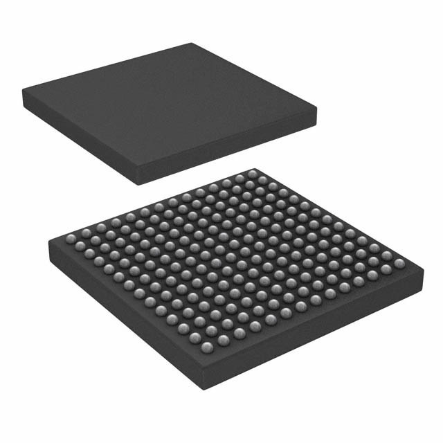


 工商网监
湘ICP备2023018690号
工商网监
湘ICP备2023018690号

