Product
Folder
Sample &
Buy
Support &
Community
Tools &
Software
Technical
Documents
ADS7251, ADS7851
SBAS587A – JANUARY 2014 – REVISED APRIL 2014
ADS7x51 12-Bit, 2-MSPS and 14-Bit, 1.5-MSPS, Dual, Differential Input, SimultaneousSampling, Analog-to-Digital Converters with Internal Reference
1 Features
3 Description
•
•
•
•
•
The ADS7251 and ADS7851 belong to a family of
pin-compatible, dual, high-speed, simultaneoussampling, analog-to-digital converters (ADCs) that
support fully-differential analog inputs and feature two
independent internal voltage references. The
ADS7251 offers 12-bit resolution and up to 2-MSPS
sampling speed. The ADS7851 offers 14-bit
resolution and up to 1.5-MSPS sampling speed.
1
•
•
•
12- and 14-Bit Pin-Compatible Family
Simultaneous Sampling of Two Channels
Supports Fully-Differential Analog Inputs
Independent Internal Reference (per ADC)
High Speed:
– Up to 2 MSPS with the ADS7251 (12-Bit)
– Up to 1.5 MSPS with the ADS7851 (14-Bit)
Excellent Performance:
– ADS7251:
– SNR: 73 dB
– INL: ±1 LSB
– ADS7851:
– SNR: 83.5 dB
– INL: ±2 LSB
Fully-Specified Over the Extended Industrial
Temperature Range: –40°C to +125°C
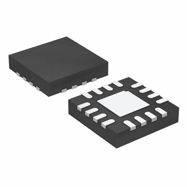
Small Footprint: WQFN-16 (3 mm × 3 mm)
The devices support a wide digital supply voltage
range, allowing easy communication with a variety of
digital host controllers using a simple, serial interface.
Both devices are fully specified over the extended
industrial temperature range (–40°C to +125°C) and
are available in a pin-compatible, space-saving,
WQFN-16 (3-mm × 3-mm) package.
Device Information
ORDER NUMBER
•
•
•
•
•
•
Motor Control: Direct Interface to SinCos
Encoders
Optical Networking: EDFA Gain Control Loop
Protection Relays
Power Quality Measurement
Three-Phase Power Controls
Programmable Logic Controllers
Industrial Automation
BODY SIZE
WQFN (16)
3 mm × 3 mm
ADS7851RTE
WQFN (16)
3 mm × 3 mm
Typical Application Diagram
2 Applications
•
PACKAGE
ADS7251RTE
C
ADS7851,
ADS7251
R
AINP
VCM
+V
+V
+V
AINM
R
C
Internal
Reference
C
R
AINP
VCM
+V
+V
+V
AINM
R
C
1
An IMPORTANT NOTICE at the end of this data sheet addresses availability, warranty, changes, use in safety-critical applications,
intellectual property matters and other important disclaimers. PRODUCTION DATA.
�ADS7251, ADS7851
SBAS587A – JANUARY 2014 – REVISED APRIL 2014
www.ti.com
Table of Contents
1
2
3
4
5
6
Features ..................................................................
Applications ...........................................................
Description .............................................................
Revision History.....................................................
Terminal Configuration and Functions................
Specifications.........................................................
6.1
6.2
6.3
6.4
6.5
6.6
6.7
6.8
6.9
6.10
6.11
6.12
7
1
1
1
2
3
4
Absolute Maximum Ratings ..................................... 4
Handling Ratings....................................................... 4
Recommended Operating Conditions....................... 4
Thermal Information .................................................. 4
Electrical Characteristics: ADS7251 ......................... 5
Electrical Characteristics: ADS7851 ......................... 6
Electrical Characteristics: Common .......................... 7
ADS7251 Timing Characteristics .............................. 8
ADS7851 Timing Characteristics .............................. 9
Typical Characteristics: ADS7251 ........................ 10
Typical Characteristics: ADS7851 ........................ 13
Typical Characteristics: Common ......................... 16
Detailed Description ............................................ 17
7.1
7.2
7.3
7.4
8
Overview .................................................................
Functional Block Diagram .......................................
Feature Description.................................................
Device Functional Modes........................................
17
17
18
21
Application and Implementation ........................ 23
8.1 Application Information............................................ 23
8.2 Typical Application ................................................. 23
9 Power Supply Recommendations...................... 27
10 Layout................................................................... 28
10.1 Layout Guidelines ................................................. 28
10.2 Layout Example .................................................... 28
11 Device and Documentation Support ................. 29
11.1
11.2
11.3
11.4
11.5
Documentation Support ........................................
Related Links ........................................................
Trademarks ...........................................................
Electrostatic Discharge Caution ............................
Glossary ................................................................
29
29
29
29
29
12 Mechanical, Packaging, and Orderable
Information ........................................................... 29
4 Revision History
Changes from Original (January 2014) to Revision A
Page
•
Changed format to meet latest data sheet standards; added Layout section, moved existing sections ............................... 1
•
Deleted Ordering Information table ........................................................................................................................................ 3
•
Changed Supply Current, IDVDD parameter typical specification in Electrical Characteristics: ADS7251 table...................... 5
•
Changed Supply Current, IDVDD parameter typical specification in Electrical Characteristics: ADS7851 table...................... 6
•
Changed Input Voltage column in Table 1 ........................................................................................................................... 20
2
Submit Documentation Feedback
Copyright © 2014, Texas Instruments Incorporated
Product Folder Links: ADS7251 ADS7851
�ADS7251, ADS7851
www.ti.com
SBAS587A – JANUARY 2014 – REVISED APRIL 2014
5 Terminal Configuration and Functions
REFOUT-A
1
REFGND-A
2
AINM-A
AINP-A
AVDD
GND
16
15
14
13
RTE Package
WQFN-16
(Top View)
12
SDO-B
11
SDO-A
REFGND-B
3
10
SCLK
REFOUT-B
4
9
CS
5
6
7
8
AINM-B
AINP-B
DVDD
GND
Thermal Pad
Terminal Descriptions
TERMINAL
NAME
NO.
I/O
AINM-A
16
Analog input
Negative analog input, channel A
DESCRIPTION
AINP-A
15
Analog input
Positive analog input, channel A
AINM-B
5
Analog input
Negative analog input, channel B
AINP-B
6
Analog input
Positive analog input, channel B
AVDD
14
Supply
CS
9
Digital input
DVDD
7
Supply
Digital I/O supply
GND
8, 13
Supply
Digital ground
REFGND-A
2
Supply
Reference ground potential, channel A
REFGND-B
3
Supply
Reference ground potential, channel B
REFOUT-A
1
Analog output
Reference voltage output, REF_A
REFOUT-B
4
Analog output
Reference voltage output, REF_B
SCLK
10
Digital input
SDO-A
11
Digital output
Data output for serial communication, channel A
SDO-B
12
Digital output
Data output for serial communication, channel B
Thermal pad
Supply
ADC supply voltage
Chip-select signal; active low
Serial communication clock
Exposed thermal pad.
TI recommends connecting this pin to the printed circuit board (PCB) ground.
Submit Documentation Feedback
Copyright © 2014, Texas Instruments Incorporated
Product Folder Links: ADS7251 ADS7851
3
�ADS7251, ADS7851
SBAS587A – JANUARY 2014 – REVISED APRIL 2014
www.ti.com
6 Specifications
6.1 Absolute Maximum Ratings (1)
over operating free-air temperature range (unless otherwise noted)
AVDD to GND
Supply voltage
DVDD to GND
Analog input voltage
MIN
MAX
UNIT
–0.3
+7
V
–0.3
+7
V
AINP_x to REFGND_x
REFGND_x – 0.3
AVDD + 0.3
V
AINM_x to REFGND_x
REFGND_x – 0.3
AVDD + 0.3
V
GND – 0.3
DVDD + 0.3
V
Digital input voltage
CS, SCLK to GND
Ground voltage difference
| REFGND_x – GND |
0.3
V
Input current
Any pin except supply pins
±10
mA
+150
°C
Maximum virtual junction temperature, TJ
(1)
Stresses beyond those listed under Absolute Maximum Ratings may cause permanent damage to the device. These are stress ratings
only, which do not imply functional operation of the device at these or any other conditions beyond those indicated under Recommended
Operating Conditions. Exposure to absolute-maximum-rated conditions for extended periods may affect device reliability.
6.2 Handling Ratings
Tstg
Storage temperature range
VESD (1),
all pins
(1)
(2)
(3)
MIN
MAX
UNIT
–65
+150
°C
Human body model (HBM) ESD stress voltage (2),
JEDEC standard 22, test method A114-C.01
±2000
V
Charged device model (CDM) ESD stress voltage (3),
JEDEC standard 22, test method C101
±500
V
Electrostatic discharge (ESD) to measure device sensitivity and immunity to damage caused by assembly line electrostatic discharges in
to the device.
Level listed above is the passing level per ANSI, ESDA, and JEDEC JS-001. JEDEC document JEP155 states that ±2000-V HBM
allows safe manufacturing with a standard ESD control process.
Level listed above is the passing level per EIA-JEDEC JESD22-C101. JEDEC document JEP157 states that ±500-V CDM allows safe
manufacturing with a standard ESD control process.
6.3 Recommended Operating Conditions
over operating free-air temperature range (unless otherwise noted)
MIN
AVDD
Analog supply voltage
DVDD
Digital supply voltage
NOM
MAX
UNIT
5
V
3.3
V
6.4 Thermal Information
THERMAL METRIC (1)
ADS7251,
ADS7851
RTE (WQFN)
UNIT
16 TERMINALS
RθJA
Junction-to-ambient thermal resistance
33.3
RθJC(top)
Junction-to-case (top) thermal resistance
29.5
RθJB
Junction-to-board thermal resistance
7.3
ψJT
Junction-to-top characterization parameter
0.2
ψJB
Junction-to-board characterization parameter
7.4
RθJC(bot)
Junction-to-case (bottom) thermal resistance
0.9
(1)
4
°C/W
For more information about traditional and new thermal metrics, see the IC Package Thermal Metrics application report, SPRA953.
Submit Documentation Feedback
Copyright © 2014, Texas Instruments Incorporated
Product Folder Links: ADS7251 ADS7851
�ADS7251, ADS7851
www.ti.com
SBAS587A – JANUARY 2014 – REVISED APRIL 2014
6.5 Electrical Characteristics: ADS7251
All minimum and maximum specifications are at TA = –40°C to +125°C, AVDD = 5 V, VREF_A = VREF_B = 2.5 V, and fDATA =
2 MSPS, unless otherwise noted. Typical values are at TA = +25°C, AVDD = 5 V, and DVDD = 3.3 V.
PARAMETER
TEST CONDITIONS
MIN
TYP
MAX
UNIT
RESOLUTION
Resolution
12
Bits
SAMPLING DYNAMICS
tCONV
Conversion time
tACQ
Acquisition time
fDATA
Data rate
fCLK
Clock frequency
tSU_CSCK + 12 tCLK
ns
75
ns
2
MSPS
32
MHz
DC ACCURACY
NMC
No missing codes
DNL
Differential nonlinearity
INL
Integral nonlinearity
VOS
Input offset error
12
VOS match
ADC_A to ADC_B
Bits
–0.99
±0.3
1
LSB
–1
±0.5
1
LSB
–1
±0.2
1
mV
–1
±0.2
1
mV
μV/°C
dVOS/dT
Input offset thermal drift
4
GE
Gain error
Referenced to the voltage at
REFOUT_x
–0.1%
±0.05%
0.1%
GERR match
ADC_A to ADC_B
–0.1%
±0.05%
0.1%
GE/dT
Gain error thermal drift
Referenced to the voltage at
REFOUT_x
CMRR
Common-mode rejection ratio
Both ADCs, dc to 20 kHz
1
ppm/°C
72
dB
72.9
dB
AC ACCURACY
SINAD
Signal-to-noise + distortion
SNR
Signal-to-noise ratio
THD
Total harmonic distortion
SFDR
Spurious-free dynamic range
72.7
For 20-kHz input frequency,
at –0.5 dBFS
Isolation between ADC_A and
ADC_B
fIN = 15 kHz, fNOISE = 25 kHz
72.8
73
dB
–90
dB
90
dB
–105
dB
SUPPLY CURRENT
IAVDD-DYNAMIC
IAVDD-STATIC
Supply
current
IDVDD
Analog, during
conversion
Throughput = 2 MSPS,
AVDD = 5 V
Analog, static
Digital, for code 800
11
12
mA
5.5
mA
0.15
mA
POWER DISSIPATION
PD-ACTIVE
PD-STATIC
Power
dissipation
During conversion
Throughput = 2 MSPS,
AVDD = 5 V
Static mode
55
60
27.5
Submit Documentation Feedback
Copyright © 2014, Texas Instruments Incorporated
Product Folder Links: ADS7251 ADS7851
mW
mW
5
�ADS7251, ADS7851
SBAS587A – JANUARY 2014 – REVISED APRIL 2014
www.ti.com
6.6 Electrical Characteristics: ADS7851
All minimum and maximum specifications are at TA = –40°C to +125°C, AVDD = 5 V, VREF_A = VREF_B = 2.5 V, and fDATA =
1.5 MSPS, unless otherwise noted. Typical values are at TA = +25°C, AVDD = 5 V, and DVDD = 3.3 V.
PARAMETER
TEST CONDITIONS
MIN
TYP
MAX
UNIT
RESOLUTION
Resolution
14
Bits
SAMPLING DYNAMICS
tCONV
Conversion time
tACQ
Acquisition time
fDATA
Data rate
fCLK
Clock frequency
tSU_CSCK + 14 tCLK
90
ns
ns
1500
kSPS
27
MHz
DC ACCURACY
NMC
No missing codes
13
DNL
Differential nonlinearity
–1
±0.75
2
LSB
INL
Integral nonlinearity
–2
±1
2
LSB
VOS
Input offset error
–1
±0.2
1
mV
–1
±0.2
1
VOS match
ADC_A to ADC_B
Bits
mV
μV/°C
dVOS/dT
Input offset thermal drift
1
GE
Gain error
Referenced to the voltage at
REFOUT_x
–0.1%
±0.05%
0.1%
GERR match
ADC_A to ADC_B
–0.1%
±0.05%
0.1%
GE/dT
Gain error thermal drift
Referenced to the voltage at
REFOUT_x
CMRR
Common-mode rejection ratio
Both ADCs, dc to 20 kHz
1
ppm/°C
72
dB
81.4
82.6
dB
82
83.5
dB
–90
dB
90
dB
–120
dB
AC ACCURACY
SINAD
Signal-to-noise + distortion
SNR
Signal-to-noise ratio
THD
Total harmonic distortion
SFDR
Spurious-free dynamic range
Isolation between ADC_A and
ADC_B
For 20-kHz input frequency,
at –0.5 dBFS
fIN = 15 kHz, fNOISE = 25 kHz
SUPPLY CURRENT
Analog, during
conversion
IAVDD-DYNAMIC
IAVDD-STATIC
Supply
current
Throughput = 1.5 MSPS,
AVDD = 5 V
Analog, static
Digital, for code
2000
IDVDD
10
12
mA
5.5
mA
0.15
mA
POWER DISSIPATION
PD-ACTIVE
PD-STATIC
6
Power
dissipation
During conversion
Throughput = 1.5 MSPS,
AVDD = 5 V
Static mode
50
27.5
Submit Documentation Feedback
60
mW
mW
Copyright © 2014, Texas Instruments Incorporated
Product Folder Links: ADS7251 ADS7851
�ADS7251, ADS7851
www.ti.com
SBAS587A – JANUARY 2014 – REVISED APRIL 2014
6.7 Electrical Characteristics: Common
All minimum and maximum specifications are at TA = –40°C to +125°C, AVDD = 5 V, VREF_A = VREF_B = 2.5 V, and fDATA =
2 MSPS, unless otherwise noted. Typical values are at TA = +25°C, AVDD = 5 V, and DVDD = 3.3 V.
PARAMETER
TEST CONDITIONS
MIN
TYP
MAX
UNIT
ANALOG INPUT
Full-scale input range
(AINP_x – AINM_x)
For AVDD ≥ 5 V
–2 VREF
2 VREF
V
For AVDD < 5 V
–AVDD
AVDD
V
VIN
Absolute input voltage
(AINP_x or AIM_x to REFGND_x)
For AVDD ≥ 5 V
0
2 VREF
V
For AVDD < 5 V
0
AVDD
V
VCM
Input common-mode voltage range
VREF_A = VREF_B = VREF
VREF – 0.1
VREF VREF + 0.1
FSR
CIN
In sample mode
Input capacitance
In hold mode
V
40
pF
4
pF
SAMPLING DYNAMICS
tA
Aperture delay
tA match
Full-power
bandwidth
BW
ADC_A to ADC_B
At 3 dB
At 0.1 dB
8
ns
40
ps
25
MHz
5
MHz
INTERNAL VOLTAGE REFERENCE
VREFOUT
Internal reference output voltage
At +25°C
VREFOUT-match VREFOUT matching
| REFOUT_A – REFOUT_B |
dVREFOUT/dt
Long-term voltage drift
1000 hours
dVREFOUT/dT
Reference voltage drift with temperature
RO
Internal reference output impedance
COUT
External output capacitor
Internal reference output settling time
DIGITAL INPUTS
2.495
COUT = 22 μF
2.500
2.505
V
±1
mV
150
ppm
±10
ppm/°C
1
Ω
22
μF
10
ms
(1)
VIH
Input voltage, high
VIL
Input voltage, low
CIN
Input capacitance
IIN
Input leakage current
0.7 DVDD
DVDD + 0.3
–0.3
0.3 DVDD
5
0 ≤ Vdigital-input ≤ DVDD
V
V
pF
1
μA
0.8 DVDD
DVDD
V
0
0.2 DVDD
V
±0.1
DIGITAL OUTPUTS (1)
VOH
Output voltage, high
IOH = 500-µA source
VOL
Output voltage, low
IOH = 500-µA sink
POWER SUPPLY
AVDD
DVDD
4.75 (2)
5.0
5.25
V
Operational range
1.65
3.3
5.25
V
For specified performance
1.65
3
3.6
V
+125
°C
Analog (AVDD to GND)
Supply voltage
Digital (DVDD to GND)
TEMPERATURE RANGE
TA
(1)
(2)
Operating free-air temperature
–40
Specified by design; not production tested.
The AVDD supply voltage defines the permissible voltage swing on the analog input pins. Refer to the Power Supply Recommendations
section for more details.
Submit Documentation Feedback
Copyright © 2014, Texas Instruments Incorporated
Product Folder Links: ADS7251 ADS7851
7
�ADS7251, ADS7851
SBAS587A – JANUARY 2014 – REVISED APRIL 2014
www.ti.com
6.8 ADS7251 Timing Characteristics
PARAMETER
TEST CONDITIONS
MIN
TYP
MAX
UNIT
2000
kSPS
32
MHz
fTHROUGHPUT
Throughput
fCLK = max
fCLK
CLOCK frequency
fTHROUGHPUT = max
tCLK
CLOCK period
fTHROUGHPUT = max
tPH_CK
CLOCK high time
0.45
0.55
tCLK
tPL_CK
CLOCK low time
0.45
0.55
tCLK
tCONV
Conversion time
tACQ
Acquisition time
tPH_CS
CS high time
tD_CKDO
tDV_CSDO
tD_CKCS
ns
tSU_CSCK + 12 tCLK
fCLK = max
75
Delay time
ns
CS falling to data enable
Last SCLK rising to CS rising
15
ns
10
ns
5
ns
CS rising to DOUT going to 3-state
10
Setup time CS falling to SCLK falling
ns
ns
30
SCLK rising edge to (next) data valid
tDZ_CSDO
tSU_CSCK
31.25
15
ns
ns
Figure 1 shows the details of the serial interface between the ADS7251 and the digital host controller.
Sample
N+1
Sample
N
tTHROUGHPUT
tCONV
tACQ
tPH_CS
CS
tSU_CSCK
SCLK
1
2
3
0
4
5
6
tSCLK
tPL_CK
7
8
9
10
11
12
tD_CKCS
13
14
tD_CKDO
tDV_CSDO
SDO-A
tPH_CK
tDZ_CSDO
0
ChA
D11
ChA
D10
ChA
D9
ChA
D8
ChA
D7
ChA
D6
ChA
D5
ChA
D4
ChA
D3
ChA
D2
ChA ChA
D1 D0
ChB
D4
ChB
D3
ChB
D2
ChB ChB
D1 D0
Data From Sample N
SDO-B
0
0
ChB
D11
ChB
D10
ChB
D9
ChB
D8
ChB
D7
ChB
D6
ChB
D5
Figure 1. ADS7251 Serial Interface Timing Diagram
8
Submit Documentation Feedback
Copyright © 2014, Texas Instruments Incorporated
Product Folder Links: ADS7251 ADS7851
�ADS7251, ADS7851
www.ti.com
SBAS587A – JANUARY 2014 – REVISED APRIL 2014
6.9 ADS7851 Timing Characteristics
PARAMETER
TEST CONDITIONS
MIN
TYP
MAX
UNIT
1500
kSPS
27
MHz
fTHROUGHPUT
Sample taken to data read
fCLK = max
fCLK
CLOCK frequency
fTHROUGHPUT = max
tCLK
CLOCK period
fTHROUGHPUT = max
tPH_CK
CLOCK high time
0.45
0.55
tCLK
tPL_CK
CLOCK low time
0.45
0.55
tCLK
tCONV
Conversion time
tACQ
Acquisition time
tPH_CS
CS high time
tD_CKDO
tDV_CSDO
tD_CKCS
ns
tSU_CSCK + 14 tCLK
fCLK = max
ns
30
ns
CS falling to data enable
Delay time
ns
90
SCLK rising edge to (next) data valid
Last SCLK rising to CS rising
tDZ_CSDO
tSU_CSCK
37
15
ns
10
ns
5
ns
CS rising to DOUT going to 3-state
10
Setup time CS falling to SCLK falling
ns
15
ns
Figure 2 shows the details of the serial interface between the ADS7851 and the digital host controller.
Sample
N+1
Sample
N
tTHROUGHPUT
tCONV
tACQ
tPH_CS
CS
tSU_CSCK
SCLK
1
2
3
SDO-A
tPL_CK
4
5
6
7
8
9
ChA
D12
ChA
D11
ChA
D10
ChA
D9
ChA
D8
ChA
D7
10
tSCLK
11
12
13
tD_CKCS
14
15
16
tD_CKDO
tDV_CSDO
0
tPH_CK
tDZ_CSDO
0
ChA
D13
ChA
D6
ChA
D5
ChA
D4
ChA
D3
ChA
D2
ChA
D1
ChA
D0
ChB
D5
ChB
D4
ChB
D3
ChB
D2
ChB
D1
ChB
D0
Data From Sample N
SDO-B
0
0
ChB
D13
ChB
D12
ChB
D11
ChB
D10
ChB
D9
ChB
D8
ChB
D7
ChB
D6
Figure 2. ADS7851 Serial Interface Timing Diagram
Submit Documentation Feedback
Copyright © 2014, Texas Instruments Incorporated
Product Folder Links: ADS7251 ADS7851
9
�ADS7251, ADS7851
SBAS587A – JANUARY 2014 – REVISED APRIL 2014
www.ti.com
6.10 Typical Characteristics: ADS7251
At TA = +25°C, AVDD = 5 V, DVDD = 3.3 V, VREF = 2.5 V (internal), and fDATA = 1 MSPS, unless otherwise noted.
0
75
Signal-to-Noise Ratio (dBFS)
Signal Power (dB)
-20
-40
-60
-80
-100
-120
-140
-160
-180
0
200
400
600
800
74
73.5
73
72.5
72
71.5
71
1000
Input Frequency
74.5
-40 -25 -10
C00
fIN = 500 kHz
75
-87
74.5
-88
Total Harmonic Distortion (dBFS)
Signal-to-Noise and Distortion (dBFS)
110 125
C00
Figure 4. SNR vs Device Temperature
74
73.5
73
72.5
72
71.5
71
5
20 35 50 65 80
Free-Air Temperature (oC)
95
-89
-90
-91
-92
-93
-94
-95
110 125
-40 -25 -10
C00
fIN = 10 kHz
5
20 35 50 65 80
Free-Air Temperature (oC)
95
110 125
C00
fIN = 10 kHz
Figure 5. SINAD vs Device Temperature
Figure 6. THD vs Device Temperature
75
Signal-to-Noise and Distortion (dBFS)
75
Signal-to-Noise Ratio (dBFS)
95
fIN = 10 kHz
Figure 3. Typical FFT for 500-kHz Input
-40 -25 -10
5
20 35 50 65 80
Free-Air Temperature (oC)
74
73
72
71
74
73
72
71
0
100
200
300
Input Frequency (kHz)
400
500
0
100
C00
200
300
Input Frequency (kHz)
400
500
C00
fIN = 10 kHz
Figure 7. SNR vs Input Frequency
10
Figure 8. SINAD vs Input Frequency
Submit Documentation Feedback
Copyright © 2014, Texas Instruments Incorporated
Product Folder Links: ADS7251 ADS7851
�ADS7251, ADS7851
www.ti.com
SBAS587A – JANUARY 2014 – REVISED APRIL 2014
Typical Characteristics: ADS7251 (continued)
At TA = +25°C, AVDD = 5 V, DVDD = 3.3 V, VREF = 2.5 V (internal), and fDATA = 1 MSPS, unless otherwise noted.
100
-87
80
Hits per Code (%FS)
Total Harmonic Distortion (dBFS)
-85
-89
-91
-93
60
40
20
-95
-97
0
0
100
200
300
Input Frequency (kHz)
400
2046
500
2047
C00
VIN-DIFF = 0 V
C01
Figure 10. DC Histogram
1
1
0.8
0.8
Integral Nonlinearity (LSB)
Differential Nonlinearity (LSB)
2050
65536 Data Points
Figure 9. THD vs Input Frequency
0.6
0.4
0.2
0
-0.2
-0.4
-0.6
0.6
0.4
0.2
0
-0.2
-0.4
-0.6
-0.8
-0.8
-1
-1
0
512
1024
1536 2048 2560 3072
ADC Output Code
3584
0
4096
512
1024
C01
Figure 11. Typical DNL
1536 2048 2560
ADC Output Code
3072
3584
4096
C01
Figure 12. Typical INL
1
1
0.75
0.75
Integral Nonlinearity (LSB)
Differential Nonlinearity (LSB)
2048
2049
ADC Output Code
0.5
0.25
0
-0.25
-0.5
-0.75
0.5
0.25
0
-0.25
-0.5
-0.75
-1
-1
-40 -25 -10
5
20 35 50 65 80
Free-Air Temperature (oC)
95
Figure 13. DNL vs Device Temperature
110 125
-40 -25 -10
C01
5
20 35 50 65 80
Free-Air Temperature (oC)
95
110 125
C01
Figure 14. INL vs Device Temperature
Submit Documentation Feedback
Copyright © 2014, Texas Instruments Incorporated
Product Folder Links: ADS7251 ADS7851
11
�ADS7251, ADS7851
SBAS587A – JANUARY 2014 – REVISED APRIL 2014
www.ti.com
Typical Characteristics: ADS7251 (continued)
1
0.1
0.75
0.075
0.5
0.05
Gain Error (%FS)
Offset Error (mV)
At TA = +25°C, AVDD = 5 V, DVDD = 3.3 V, VREF = 2.5 V (internal), and fDATA = 1 MSPS, unless otherwise noted.
0.25
0
-0.25
-0.5
-0.75
0.025
0
-0.025
-0.05
-0.075
-1
-0.1
-40 -25 -10
5
20
35
50
65
80
95
110 125
Free-Air Temperature (oC)
-40 -25 -10
C01
12
11.75
11
11.5
11.25
11
10.75
10.5
10.25
110 125
C01
10
9
8
7
6
5
10
-40 -25 -10
5
20 35 50 65 80
Free-Air Temperature (oC)
95
110 125
4
0
C02
Figure 17. IAVDD vs Device Temperature
12
95
Figure 16. Gain Error vs Device Temperature
12
IAVDD - Dynamic (mA)
IAVDD - Dynamic (mA)
Figure 15. Offset Error vs Device Temperature
5
20 35 50 65 80
Free-Air Temperature (oC)
Submit Documentation Feedback
500
1000
Throughput (kSPS)
1500
2000
C02
Figure 18. IAVDD vs Throughput
Copyright © 2014, Texas Instruments Incorporated
Product Folder Links: ADS7251 ADS7851
�ADS7251, ADS7851
www.ti.com
SBAS587A – JANUARY 2014 – REVISED APRIL 2014
6.11 Typical Characteristics: ADS7851
At TA = +25°C, AVDD = 5 V, DVDD = 3.3 V, VREF = 2.5 V (internal), and fDATA = 1 MSPS, unless otherwise noted.
85
84.5
Signal-to-Noise Ratio (dBFS)
0
-20
Signal Power (dB)
-40
-60
-80
-100
-120
-140
-160
-180
-200
84
83.5
83
82.5
82
81.5
81
0
150
300
450
Input Frequency (kHz)
600
-40 -25 -10
750
C02
fIN = 500 kHz
110 125
C02
Figure 20. SNR vs Device Temperature
-91
Total Harmonic Distortion (dBFS)
85
Signal-to-Noise and Distortion (dBFS)
95
fIN = 10 kHz
Figure 19. Typical FFT for 500-kHz Input
84.5
84
83.5
83
82.5
82
81.5
-91.5
-92
-92.5
-93
-93.5
-94
-94.5
-95
81
-40 -25 -10
5
20 35 50 65 80
Free-Air Temperature (oC)
95
-40 -25 -10
110 125
C02
fIN = 10 kHz
5
20 35 50 65 80
Free-Air Temperature (oC)
95
110 125
C02
fIN = 10 kHz
Figure 21. SINAD vs Device Temperature
Figure 22. THD vs Device Temperature
84
Signal-to-Noise and Distortion (dBFS)
85
Signal-to-Noise Ratio (dBFS)
5
20 35 50 65 80
Free-Air Temperature (oC)
84.5
84
83.5
83
82.5
82
81.5
83.5
83
82.5
82
81.5
81
80.5
80
81
0
100
200
300
Input Frequency (kHz)
400
500
0
100
200
300
400
Input Frequency (kHz)
C02
500
C02
fIN = 10 kHz
Figure 23. SNR vs Input Frequency
Figure 24. SINAD vs Input Frequency
Submit Documentation Feedback
Copyright © 2014, Texas Instruments Incorporated
Product Folder Links: ADS7251 ADS7851
13
�ADS7251, ADS7851
SBAS587A – JANUARY 2014 – REVISED APRIL 2014
www.ti.com
Typical Characteristics: ADS7851 (continued)
At TA = +25°C, AVDD = 5 V, DVDD = 3.3 V, VREF = 2.5 V (internal), and fDATA = 1 MSPS, unless otherwise noted.
100
-87
Hits Per Code (%FS)
Total Harmonic Distortion (dBFS)
-86
-88
-89
-90
-91
-92
80
60
40
20
-93
-94
0
100
200
300
Input Frequency (kHz)
400
0
500
8190
8191
VIN-DIFF = 0 V
1
0.8
0.8
Typical Integral Nonlinearity (LSB)
Typical Differential Nonlinearity (LSB)
8196
C03
Figure 26. DC Histogram
1
0.6
0.4
0.2
0
-0.2
-0.4
-0.6
-0.8
-1
0.6
0.4
0.2
0
-0.2
-0.4
-0.6
-0.8
-1
0
4096
8192
ADC Output Code
12288
16384
0
4096
8192
12288
ADC Output Code
C03
Figure 27. Typical DNL
16384
C03
Figure 28. Typical INL
2
2
1.5
1.5
Integral Nonlinearity (LSB)
Differential Nonlinearity (LSB)
8195
65536 Data Points
Figure 25. THD vs Input Frequency
1
0.5
0
-0.5
1
0.5
0
-0.5
-1
-1.5
-2
-1
-40 -25 -10
5
20 35 50 65 80
Free-Air Temperature (oC)
95
Figure 29. DNL vs Device Temperature
14
8192
8193
8194
ADC Output Code
C03
110 125
-40 -25 -10
C03
5
20 35 50 65 80
Free-Air Temperature (oC)
95
110 125
C04
Figure 30. INL vs Device Temperature
Submit Documentation Feedback
Copyright © 2014, Texas Instruments Incorporated
Product Folder Links: ADS7251 ADS7851
�ADS7251, ADS7851
www.ti.com
SBAS587A – JANUARY 2014 – REVISED APRIL 2014
Typical Characteristics: ADS7851 (continued)
1
0.1
0.75
0.075
0.5
0.05
Gain Error (%FS)
Offset Error (mV)
At TA = +25°C, AVDD = 5 V, DVDD = 3.3 V, VREF = 2.5 V (internal), and fDATA = 1 MSPS, unless otherwise noted.
0.25
0
-0.25
0.025
0
-0.025
-0.5
-0.05
-0.75
-0.075
-0.1
-1
-40 -25 -10
5
20 35 50 65 80
Free-Air Temperature (oC)
95
-40 -25 -10
110 125
C03
Figure 31. Offset Error vs Device Temperature
95
110 125
C03
Figure 32. Gain Error vs Device Temperature
10
12
11.5
IAVDD - Dynamic Current (mA)
IAVDD Dynamic Current (mA)
5
20 35 50 65 80
Free-Air Temperature (oC)
11
10.5
10
9.5
9
8.5
9
8
7
6
5
4
8
-40 -25 -10
5
20 35 50 65 80
Free-Air Temperature (oC)
95
110 125
0
C04
Figure 33. IAVDD vs Device Temperature
500
1000
Throughtput (kSPS)
Product Folder Links: ADS7251 ADS7851
C04
Figure 34. IAVDD vs Throughput
Submit Documentation Feedback
Copyright © 2014, Texas Instruments Incorporated
1500
15
�ADS7251, ADS7851
SBAS587A – JANUARY 2014 – REVISED APRIL 2014
www.ti.com
6.12 Typical Characteristics: Common
2.502
30
2.5015
25
2.501
20
2.5005
Current (mA)
Reference Output (V)
At TA = +25°C, AVDD = 5 V, DVDD = 3.3 V, and VREF = 2.5 V (internal), unless otherwise noted.
2.5
2.4995
15
10
5
2.499
0
2.4985
-5
2.498
-40 -25 -10
5
20 35 50 65 80
Free-Air Temperature (oC)
95
110 125
-10
2.49
2.495
2.5
C03
2.505
Voltage (V)
2.51
2.515
2.52
C03
Rout = 0.75 Ω Typ
Figure 35. Reference Output vs
Device Temperature
Figure 36. Internal Reference:
Output Current vs Output Voltage
Common-mode Rejection Ratio (dB)
110
100
90
80
70
60
50
40
0
100
200
300
Input Frequency (kHz)
400
500
C04
Figure 37. CMRR vs Input Frequency
16
Submit Documentation Feedback
Copyright © 2014, Texas Instruments Incorporated
Product Folder Links: ADS7251 ADS7851
�ADS7251, ADS7851
www.ti.com
SBAS587A – JANUARY 2014 – REVISED APRIL 2014
7 Detailed Description
7.1 Overview
The ADS7251 and ADS7851 are pin-compatible, dual, simultaneous-sampling, analog-to-digital converters
(ADCs). Each device features two independent internal voltage references and supports fully-differential input
signals with the input common-mode on each input pin equal to the reference voltage. The full-scale input signal
on each input pin is equal to twice the reference voltage. The devices provide a simple, serial interface to the
host controller and operate over a wide range of digital power supplies.
7.2 Functional Block Diagram
REF_A
Comparator
S/H
CDAC
SAR
ADC_A
ADC_B
S/H
Serial
Interface
SAR
CDAC
Comparator
REF_B
Submit Documentation Feedback
Copyright © 2014, Texas Instruments Incorporated
Product Folder Links: ADS7251 ADS7851
17
�ADS7251, ADS7851
SBAS587A – JANUARY 2014 – REVISED APRIL 2014
www.ti.com
7.3 Feature Description
7.3.1 Reference
The device has two simultaneous sampling ADCs (ADC_A and ADC_B) and two independent internal reference
sources (INTREF_A and INTREF_B). INTREF_A outputs voltage VREF_A on pin REFOUT_A and INTREF_B
outputs voltage VREF_B on pin REFOUT_B. As shown in Figure 38, the REFOUT_A and REFOUT_B pins must
be decoupled with the REFGND_A and REFGND_B pins, respectively, with individual 22-µF decoupling
capacitors. ADC_A operates with reference voltage VREF_A and ADC_B operates with reference voltage VREF_B.
AINP_A
AINM_A
ADC_A
REFGND_A
22 PF
REFOUT_A
INTREF_A
REFOUT_B
INTREF_B
22 PF
REFGND_B
AINP_B
AINM_B
ADC_B
Figure 38. Reference Block Diagram
18
Submit Documentation Feedback
Copyright © 2014, Texas Instruments Incorporated
Product Folder Links: ADS7251 ADS7851
�ADS7251, ADS7851
www.ti.com
SBAS587A – JANUARY 2014 – REVISED APRIL 2014
Feature Description (continued)
7.3.2 Analog Input
The devices support fully-differential analog input signals. These inputs are sampled and converted
simultaneously by the two ADCs, ADC_A and ADC_B. Figure 39a and Figure 39b show equivalent circuits for
the ADC_A and ADC_B analog input pins, respectively.
Series resistance (RS) represents the on-state sampling switch resistance (typically 50 Ω) and CSAMPLE is the
device sampling capacitor (typically 40 pF). ADC_A samples VAINP_A and VAINM_A and converts for the difference
voltage (VAINP_A – VAINM_A). ADC_B samples VAINP_B and VAINM_B and converts for the difference voltage
(VAINP_B – VAINM_B).
AVDD
AVDD
RS
CSAMPLE
AINP_A
RS
CSAMPLE
RS
CSAMPLE
AINP_B
GND
GND
AVDD
AVDD
RS
AINM_A
CSAMPLE
AINM_B
GND
GND
a) ADC_A
b) ADC_B
Figure 39. Equivalent Circuit for the Analog Input Pins
7.3.2.1 Analog Input Full-Scale Range
The analog input full-scale range (FSR) for ADC_A and ADC_B is twice the reference voltage provided to the
particular ADC. Therefore, the FSR for ADC_A and ADC_B can be determined by Equation 1 and Equation 2,
respectively:
FSR_ADC_A = 2 × VREF_A,
VAINP_A and VAINM_A = 0 to 2 × VREF_A,
(1)
FSR_ADC_B = 2 × VREF_B,
VAINP_B and VAINM_B = 0 to 2 × VREFIN_B
(2)
To use the full dynamic input range on the analog input pins, AVDD must be as shown in Equation 3, Equation 4,
and Equation 5:
AVDD ≥ 2 × VREF_A
AVDD ≥ 2 × VREF_B
4.5 V ≤ AVDD ≤ 5.5 V
(3)
(4)
(5)
7.3.2.2 Common-Mode Voltage Range
For the analog input, the devices support a common-mode voltage equal to the reference voltage provided to the
ADC. Therefore, the common-mode voltage for the ADC_A and ADC_B must be as shown in Equation 6 and
Equation 7, respectively.
VCM_A = VREF_A
VCM_B = VREF_B
(6)
(7)
Submit Documentation Feedback
Copyright © 2014, Texas Instruments Incorporated
Product Folder Links: ADS7251 ADS7851
19
�ADS7251, ADS7851
SBAS587A – JANUARY 2014 – REVISED APRIL 2014
www.ti.com
Feature Description (continued)
7.3.3 ADC Transfer Function
The device output is in twos compliment format. Device resolution for the fully-differential input can be computed
by Equation 8:
1 LSB = (4 × VREF) / (2N)
where:
•
•
VREF = VREF_A = VREF_B, and
N = 12 (ADS7251), or 14 (ADS7851).
(8)
Table 1 shows the different input voltages and the corresponding device output codes. Figure 40 shows the ideal
transfer characteristics for the device.
Table 1. Transfer Characteristics
OUTPUT CODE (Hex)
INPUT VOLTAGE
(AINP_x – AINM_x)
CODE
ADS7251
ADS7851
2000
< –2 × VREF
NFSC
800
–2 × VREF + 1 LSB
NFSC + 1
801
2001
–1 LSB
MC
FFF
3FFF
0
PLC
000
0000
> 2 × VREF – 1 LSB
PFSC
7FF
1FFF
ADC Code (Hex)
PFSC
PLC
MC
NFSC + 1
NFSC
NFSR + 1 LSB
�1 LSB
0
VIN
PFSR ± 1 LSB
Fully-Differential Analog Input
(AINP_x ± AINM_x)
Figure 40. Ideal Transfer Characteristics
20
Submit Documentation Feedback
Copyright © 2014, Texas Instruments Incorporated
Product Folder Links: ADS7251 ADS7851
�ADS7251, ADS7851
www.ti.com
SBAS587A – JANUARY 2014 – REVISED APRIL 2014
7.4 Device Functional Modes
7.4.1 Serial Interface
The devices support a simple, SPI-compatible interface to the external digital host. The CS signal defines one
conversion and serial transfer frame. A frame starts with a CS falling edge and ends with a CS rising edge. The
SDO_A and SDO_B pins output the ADC_A and ADC_B conversion results, respectively. Figure 41 shows a
detailed timing diagram for the ADS7251.
Sample
N+1
Sample
N
tTHROUGHPUT
tCONV
tACQ
CS
SCLK
1
SDO-A
0
2
3
4
ChA
D11
0
5
ChA
D10
6
ChA
D9
7
ChA
D8
8
ChA
D7
9
ChA
D6
10
ChA
D5
11
12
13
14
ChA
D4
ChA
D3
ChA
D2
ChA ChA
D1 D0
ChB
D4
ChB
D3
ChB
D2
ChB ChB
D1 D0
Data From Sample N
0
SDO-B
ChB
D11
0
ChB
D10
ChB
D9
ChB
D8
ChB
D7
ChB
D6
ChB
D5
Figure 41. ADS7251 Serial Interface Timing Diagram
Figure 42 shows a detailed timing diagram for the ADS7851.
Sample
N+1
Sample
N
tTHROUGHPUT
tCONV
tACQ
CS
SCLK
1
SDO-A
0
2
0
3
4
5
6
7
8
9
ChA
D13
ChA
D12
ChA
D11
ChA
D10
ChA
D9
ChA
D8
ChA
D7
10
ChA
D6
11
12
13
14
15
16
ChA
D5
ChA
D4
ChA
D3
ChA
D2
ChA
D1
ChA
D0
ChB
D5
ChB
D4
ChB
D3
ChB
D2
ChB
D1
ChB
D0
Data From Sample N
SDO-B
0
0
ChB
D13
ChB
D12
ChB
D11
ChB
D10
ChB
D9
ChB
D8
ChB
D7
ChB
D6
Figure 42. ADS7851 Serial Interface Timing Diagram
Submit Documentation Feedback
Copyright © 2014, Texas Instruments Incorporated
Product Folder Links: ADS7251 ADS7851
21
�ADS7251, ADS7851
SBAS587A – JANUARY 2014 – REVISED APRIL 2014
www.ti.com
Device Functional Modes (continued)
A CS falling edge brings the serial data bus out of 3-state and also outputs '0' on the SDO_A and SDO_B pins. A
minimum delay of tSU_CSCK must elapse between the CS falling edge and the first SCLK falling edge. The
subsequent clock edges are used to shift out the conversion result using the serial interface, as shown in
Table 2. The sample-and-hold circuit returns to sample mode as soon as the conversion process is over. Any
extra clock edges output a '0' on the SDO pins. A CS rising edge ends the frame and brings the serial data bus
to 3-state.
Table 2. Data Launch Edge
LAUNCH EDGE
SCLK
DEVICE
ADS7851
ADS7251
CS↑
PIN
CS↓
↓1
↓2
…
↓13
↓14
↓15
↓16
…
SDO-A
0
0
D13_A
…
D2_A
D1_A
D0_A
0
…
Hi-Z
SDO-B
0
0
D13_B
…
D2_B
D1_B
D0_B
0
…
Hi-Z
SDO-A
0
0
D11_A
…
D0_A
0
0
0
…
Hi-Z
SDO-B
0
0
D11_B
…
D0_B
0
0
0
…
Hi-Z
7.4.2 Short-Cycling Feature
For the ADS7851, a minimum of 16 SCLK rising edges must be provided between the beginning and end of the
frame to complete the 14-bit data transfer. For the ADS7251, a minimum of 14 SCLK rising edges must be
provided between the beginning and end of the frame to complete the 12-bit data transfer. As shown in
Figure 43, if CS is brought high before the expected number of SCLK rising edges are provided, the current
frame is aborted and the device starts sampling the new analog input signal. However, the output data bits
latched into the digital host before this CS rising edge are still valid data corresponding to sample N.
After aborting the current frame, CS must be kept high for tACQ to ensure minimum acquisition time is provided
for the next conversion.
Sample
N
Sample
N+1
tACQ
CS
SCLK
SDO
ADS7251
1
0
2
0
3
D11
D10
Data From Sample N
SDO
ADS7851
0
0
D13
D12
Figure 43. Short-Cycling Feature
22
Submit Documentation Feedback
Copyright © 2014, Texas Instruments Incorporated
Product Folder Links: ADS7251 ADS7851
�ADS7251, ADS7851
www.ti.com
SBAS587A – JANUARY 2014 – REVISED APRIL 2014
8 Application and Implementation
8.1 Application Information
The two primary circuits required to maximize the performance of a high-precision, successive approximation
register (SAR), analog-to-digital converter (ADC) are the input driver and the reference driver circuits. The
ADS7851 and ADS7251 feature an internal reference designed to support device requirements. This section
details some general principles for designing the input driver circuit and provides some application circuits
designed using these devices.
8.2 Typical Application
The application circuit shown in Figure 44 is optimized for using the ADS7251 at a 2-MSPS throughput to
achieve lowest distortion and lowest noise for input signal frequencies up to 100 kHz.
1 K
�
1 K
�
AVDD
AVDD
VIN+
VREF
VCM
+
+
THS4521
+
-
10
�
820 pF
AVDD
V
AINP
+
ADS7251
AINM
GND
10
�
+
VIN-
1 K
�
1 K
�
AD7251 2 MSPS
32MHz SCLK
INPUT DRIVER
Figure 44. ADS7251 DAQ Circuit: Maximum SINAD for Input Signal Frequencies up to 100 kHz
The application circuit shown in Figure 45 is optimized for using the ADS7851 at a 1.5-MSPS throughput to
achieve lowest distortion and lowest noise for input signal frequencies up to 100 kHz.
1 K
�
1 K
�
AVDD
AVDD
VIN+
VREF
VCM
+
+
THS4521
+
-
10
�
820 pF
V
AINP
+
ADS7851
AINM
GND
10
�
+
VIN-
AVDD
1 K
�
1 K
�
INPUT DRIVER
AD7851 1.5 MSPS
27MHz SCLK
Figure 45. ADS7851 DAQ Circuit: Maximum SINAD for Input Signal Frequencies up to 100 kHz
Submit Documentation Feedback
Copyright © 2014, Texas Instruments Incorporated
Product Folder Links: ADS7251 ADS7851
23
�ADS7251, ADS7851
SBAS587A – JANUARY 2014 – REVISED APRIL 2014
www.ti.com
Typical Application (continued)
8.2.1 Design Requirements
For the ADS7251, design an input driver and reference driver circuit to achieve > 71-dB SNR and < –90-dB THD
at input frequencies of 10 kHz and 100 kHz.
For the ADS7851, design an input driver and reference driver circuit to achieve > 81-dB SNR and < –90-dB THD
at input frequencies of 10 kHz and 100 kHz.
8.2.2 Detailed Design Procedure
The input driver circuit for a high-precision ADC mainly consists of two parts: a driving amplifier and an
antialiasing filter. Careful design of the front-end circuit is critical to meet the linearity and noise performance of a
high-precision ADC.
8.2.2.1 Input Amplifier Selection
Selection criteria for the input amplifiers is highly dependent on the input signal type and the performance goals
of the data acquisition system. Some key amplifier specifications to consider while selecting an appropriate
amplifier to drive the inputs of the ADC are:
• Small-signal bandwidth. Select the small-signal bandwidth of the input amplifiers to be as high as possible
after meeting the power budget of the system. Higher bandwidth reduces the closed-loop output impedance
of the amplifier, thus allowing the amplifier to more easily drive the low cutoff frequency RC filter at the ADC
inputs. Higher bandwidth also minimizes the harmonic distortion at higher input frequencies. In order to
maintain the overall stability of the input driver circuit, the amplifier bandwidth should be selected as
described in Equation 9:
•
§
·
1
¸¸
Unity � Gain Bandwidth t 4 u ¨¨
© 2S u RFLT u CFLT ¹
(9)
Noise. Noise contribution of the front-end amplifiers should be as low as possible to prevent any degradation
in SNR performance of the system. As a rule of thumb, to ensure that the noise performance of the data
acquisition system is not limited by the front-end circuit, the total noise contribution from the front-end circuit
should be kept below 20% of the input-referred noise of the ADC. Noise from the input driver circuit is
bandlimited by designing a low cutoff frequency RC filter, as explained in Equation 10.
2
§ V 1 _ AM P_ PP ·
S
¨
¸
NG u 2 u ¨ f
� en2 _ RM S u u f�3dB
¸
6.6
2
¨
¸
©
¹
d
§ SNR�dB� ·
¸
20
¹
�¨
1 VREF
u
u 10 ©
5
2
where:
•
•
•
•
•
V1 / f_AMP_PP is the peak-to-peak flicker noise in µVRMS,
en_RMS is the amplifier broadband noise density in nV/√Hz,
f–3dB is the 3-dB bandwidth of the RC filter, and
NG is the noise gain of the front-end circuit, which is equal to '1' in a buffer configuration.
Distortion. Both the ADC and the input driver introduce nonlinearity in a data acquisition block. As a rule of
thumb, to ensure that the distortion performance of the data acquisition system is not limited by the front-end
circuit, the distortion of the input driver should be at least 10 dB lower than the distortion of the ADC, as
shown in Equation 11.
THD AMP d THD ADC � 10 �dB �
•
24
(10)
(11)
Settling Time. For dc signals with fast transients that are common in a multiplexed application, the input signal
must settle to the desired accuracy at the inputs of the ADC during the acquisition time window. This
condition is critical to maintain the overall linearity performance of the ADC. Typically, the amplifier data
sheets specify the output settling performance only up to 0.1% to 0.001%, which may not be sufficient for the
desired accuracy. Therefore, the settling behavior of the input driver should always be verified by TINA™SPICE simulations before selecting the amplifier.
Submit Documentation Feedback
Copyright © 2014, Texas Instruments Incorporated
Product Folder Links: ADS7251 ADS7851
�ADS7251, ADS7851
www.ti.com
SBAS587A – JANUARY 2014 – REVISED APRIL 2014
Typical Application (continued)
The distortion resulting from variation in the common-mode signal is eliminated by using a fully-differential
amplifier (FDA) in an inverting gain configuration that establishes a fixed common-mode level at the ADC input.
This configuration also eliminates the requirement of rail-to-rail swing at the amplifier input. The low-power
THS4521, used as an input driver, provides exceptional ac performance because of its extremely low-distortion
and high-bandwidth specifications. The device REFOUT_x pin can be directly connected to the VOCM pin of the
THS4521 to set the output common-mode voltage to 2.5 V, as required by the ADC.
8.2.2.2 Antialiasing Filter
Converting analog-to-digital signals requires sampling an input signal at a constant rate. Any higher frequency
content in the input signal beyond half the sampling frequency is digitized and folded back into the low-frequency
spectrum. This process is called aliasing. Therefore, an analog, antialiasing filter must be used to remove the
harmonic content from the input signal before being sampled by the ADC. An antialiasing filter is designed as a
low-pass, RC filter, for which the 3-dB bandwidth is optimized based on specific application requirements (as
shown in Figure 46). For dc signals with fast transients (including multiplexed input signals), a high-bandwidth
filter is designed to allow accurately settling the signal at the ADC inputs during the small acquisition time
window. For ac signals, the filter bandwidth should be kept low to band-limit the noise fed into the ADC input,
thereby increasing the signal-to-noise ratio (SNR) of the system.
Besides filtering the noise from the front-end drive circuitry, the RC filter also helps attenuate the sampling
charge injection from the switched-capacitor input stage of the ADC. A filter capacitor, CFLT, is connected across
the ADC inputs. This capacitor helps reduce the sampling charge injection and provides a charge bucket to
quickly charge the internal sample-and-hold capacitors during the acquisition process. As a rule of thumb, the
value of this capacitor should be at least 10 times the specified value of the ADC sampling capacitance. For
these devices, the input sampling capacitance is equal to 40 pF. Thus, the value of CFLT should be greater than
400 pF. The capacitor should be a COG- or NPO-type because these capacitor types have a high-Q, lowtemperature coefficient, and stable electrical characteristics under varying voltages, frequency, and time.
Note that driving capacitive loads can degrade the phase margin of the input amplifiers, thus making the amplifier
marginally unstable. To avoid amplifier stability issues, series isolation resistors (RFLT) are used at the output of
the amplifiers. A higher value of RFLT is helpful from the amplifier stability perspective, but adds distortion as a
result of interactions with the nonlinear input impedance of the ADC. Distortion increases with source impedance,
input signal frequency, and input signal amplitude. Therefore, the selection of RFLT requires balancing the stability
and distortion of the design. For these devices, TI recommends limiting the value of RFLT to a maximum of 22 Ω
in order to avoid any significant degradation in linearity performance. The tolerance of the selected resistors can
be chosen as 1% because the use of a differential capacitor at the input balances the effects resulting from any
resistor mismatch.
RFLT �22
�
f � 3 dB
2S u �R FLT
1
� R FLT � u C FLT
CFLT ��400 pF
VAINP
+ ADS7851
ADS7251
AINM
GND
RFLT �22
�
Figure 46. Antialiasing Filter
The input amplifier bandwidth should be much higher than the cutoff frequency of the antialiasing filter. TI
strongly recommends performing a SPICE simulation to confirm that the amplifier has more than 40° phase
margin with the selected filter. Simulation is critical because even with high-bandwidth amplifiers, some amplifiers
might require more bandwidth than others to drive similar filters. If an amplifier has less than a 40° phase margin
with 22-Ω resistors, using a different amplifier with higher bandwidth or reducing the filter cutoff frequency with a
larger differential capacitor is advisable.
In addition, the components of the antialiasing filter are such that the noise from the front-end circuit is kept low
without adding distortion to the input signal.
Submit Documentation Feedback
Copyright © 2014, Texas Instruments Incorporated
Product Folder Links: ADS7251 ADS7851
25
�ADS7251, ADS7851
SBAS587A – JANUARY 2014 – REVISED APRIL 2014
www.ti.com
Typical Application (continued)
8.2.3 Application Curves
Figure 47 shows an FFT plot for the ADS7251 with the circuit shown in Figure 44 and an input frequency of
10 kHz. Figure 48 shows an FFT plot for the ADS7251 with the same circuit configuration but for an input
frequency of 100 kHz.
0
0
AVDD = 5 V
TA = 25oC
fIN = 10 kHz
SNR = 73 dB
THD = -90 dB
-20
-40
-60
Power (dB)
Power (dB)
-40
AVDD = 5 V
TA = 25oC
fIN = 100 kHz
SNR = 72 dB
THD = -91 dB
-20
-80
-100
-60
-80
-100
-120
-120
-140
-140
-160
-160
0
200
400
600
800
1000
Input Frequency (kHz)
0
200
C10
Figure 47. Test Results for ADS7251 with a 10-kHz Input
400
600
Input Frequency (kHz)
800
1000
C10
Figure 48. Test Results for ADS7251 with a 100-kHz Input
Figure 49 shows an FFT plot for the ADS7851 with the circuit shown in Figure 45 and an input frequency of
10 kHz. Figure 50 shows an FFT plot for the ADS7251 with the same circuit configuration but for an input
frequency of 100 kHz.
0
0
AVDD = 5 V
TA = 25oC
fIN = 10 kHz
SNR = 82.3 dB
THD = -91 dB
-20
-60
-40
Power (dB)
Power (dB)
-40
-80
-100
-60
-80
-100
-120
-120
-140
-140
-160
-160
0
150
300
450
600
Input Frequency (kHz)
750
0
150
300
450
600
750
Input Frequency (kHz)
C10
Figure 49. Test Results with a 10-kHz Input
26
AVDD = 5 V
TA = 25oC
fIN = 100 kHz
SNR = 82.3 dB
THD = -93 dB
-20
C10
Figure 50. Test Results with a 100-kHz Input
Submit Documentation Feedback
Copyright © 2014, Texas Instruments Incorporated
Product Folder Links: ADS7251 ADS7851
�ADS7251, ADS7851
www.ti.com
SBAS587A – JANUARY 2014 – REVISED APRIL 2014
9 Power Supply Recommendations
The devices have two separate power supplies: AVDD and DVDD. The device operates on AVDD; DVDD is
used for the interface circuits. AVDD and DVDD can be independently set to any value within the permissible
ranges.
The AVDD supply voltage value defines the permissible voltage swing on the analog input pins. To avoid
saturation of output codes, and to use the full dynamic range on the analog input pins, AVDD must be set as
shown in Equation 12, Equation 13, and Equation 14:
AVDD ≥ 2 × VREF_A
AVDD ≥ 2 × VREF_B
4.75 V ≤ AVDD ≤ 5.25 V
(12)
(13)
(14)
Decouple the AVDD and DVDD pins with the GND pin using individual 10-µF decoupling capacitors, as shown in
Figure 51.
AVDD
AVDD (pin 14)
10 PF
GND (pin 13)
10 PF
DVDD
DVDD (pin 7)
Figure 51. Power-Supply Decoupling
Submit Documentation Feedback
Copyright © 2014, Texas Instruments Incorporated
Product Folder Links: ADS7251 ADS7851
27
�ADS7251, ADS7851
SBAS587A – JANUARY 2014 – REVISED APRIL 2014
www.ti.com
10 Layout
10.1 Layout Guidelines
Figure 52 shows a board layout example for the ADS7251 and ADS7851. Use a ground plane underneath the
device and partition the PCB into analog and digital sections. Avoid crossing digital lines with the analog signal
path and keep the analog input signals and the reference input signals away from noise sources. As shown in
Figure 52, the analog input and reference signals are routed on the left side of the board and the digital
connections are routed on the right side of the device.
The power sources to the device must be clean and well-bypassed. Use 10-μF, ceramic bypass capacitors in
close proximity to the analog (AVDD) and digital (DVDD) power-supply pins. Avoid placing vias between the
AVDD and DVDD pins and the bypass capacitors. Connect all ground pins to the ground plane using short, lowimpedance paths.
The REFOUT-A and REFOUT-B reference outputs are bypassed with 10-μF, X7R-grade ceramic capacitors
(CREF-x). Place the reference bypass capacitors as close as possible to the reference REFOUT-x pins and
connect the bypass capacitors using short, low-inductance connections. Avoid placing vias between the
REFOUT-x pins and the bypass capacitors. Small 0.1-Ω to 0.2-Ω resistors (RREF-x) are used in series with the
reference bypass capacitors to improve stability.
The fly-wheel RC filters are placed immediately next to the input pins. Among ceramic surface-mount capacitors,
COG (NPO) ceramic capacitors provide the best capacitance precision. The type of dielectric used in COG
(NPO) ceramic capacitors provides the most stable electrical properties over voltage, frequency, and temperature
changes. Figure 52 shows CIN-A and CIN-B filter capacitors placed across the analog input pins of the device.
10.2 Layout Example
CREF-A
AVDD
CIN-A
GND
GND
AVDD
AINP-A
AINM-A
GND
RREF-A
CAVDD
SDO-A
REFOUT-A
CREF-B
SCLK
CIN-B
GND
/CS
GND
AINM-B
RREF-B
REFOUT-B
GND
SDO-B
REFGND-B
DVDD
GND
REFGND-A
AINP-B
GND
CDVDD
DVDD
GND
GND
Figure 52. Example Layout for the ADS7251 and ADS7851
28
Submit Documentation Feedback
Copyright © 2014, Texas Instruments Incorporated
Product Folder Links: ADS7251 ADS7851
�ADS7251, ADS7851
www.ti.com
SBAS587A – JANUARY 2014 – REVISED APRIL 2014
11 Device and Documentation Support
11.1 Documentation Support
11.1.1 Related Documentation
For related documentation see the following:
• THS4521 Data Sheet, SBOS458
11.2 Related Links
The table below lists quick access links. Categories include technical documents, support and community
resources, tools and software, and quick access to sample or buy.
Table 3. Related Links
PARTS
PRODUCT FOLDER
SAMPLE & BUY
TECHNICAL
DOCUMENTS
TOOLS &
SOFTWARE
SUPPORT &
COMMUNITY
ADS7251
Click here
Click here
Click here
Click here
Click here
ADS7851
Click here
Click here
Click here
Click here
Click here
11.3 Trademarks
TINA is a trademark of Texas Instruments Inc..
All other trademarks are the property of their respective owners.
11.4 Electrostatic Discharge Caution
These devices have limited built-in ESD protection. The leads should be shorted together or the device placed in conductive foam
during storage or handling to prevent electrostatic damage to the MOS gates.
11.5 Glossary
SLYZ022 — TI Glossary.
This glossary lists and explains terms, acronyms and definitions.
12 Mechanical, Packaging, and Orderable Information
The following pages include mechanical, packaging, and orderable information. This information is the most
current data available for the designated devices. This data is subject to change without notice and revision of
this document. For browser-based versions of this data sheet, refer to the left-hand navigation.
Submit Documentation Feedback
Copyright © 2014, Texas Instruments Incorporated
Product Folder Links: ADS7251 ADS7851
29
�PACKAGE OPTION ADDENDUM
www.ti.com
10-Dec-2020
PACKAGING INFORMATION
Orderable Device
Status
(1)
Package Type Package Pins Package
Drawing
Qty
Eco Plan
(2)
Lead finish/
Ball material
MSL Peak Temp
Op Temp (°C)
Device Marking
(3)
(4/5)
(6)
ADS7251IRTER
ACTIVE
WQFN
RTE
16
3000
RoHS & Green
NIPDAU
Level-2-260C-1 YEAR
-40 to 125
7251
ADS7251IRTET
ACTIVE
WQFN
RTE
16
250
RoHS & Green
NIPDAU
Level-2-260C-1 YEAR
-40 to 125
7251
ADS7851IRTER
ACTIVE
WQFN
RTE
16
3000
RoHS & Green
NIPDAU
Level-2-260C-1 YEAR
-40 to 125
7851
ADS7851IRTET
ACTIVE
WQFN
RTE
16
250
RoHS & Green
NIPDAU
Level-2-260C-1 YEAR
-40 to 125
7851
(1)
The marketing status values are defined as follows:
ACTIVE: Product device recommended for new designs.
LIFEBUY: TI has announced that the device will be discontinued, and a lifetime-buy period is in effect.
NRND: Not recommended for new designs. Device is in production to support existing customers, but TI does not recommend using this part in a new design.
PREVIEW: Device has been announced but is not in production. Samples may or may not be available.
OBSOLETE: TI has discontinued the production of the device.
(2)
RoHS: TI defines "RoHS" to mean semiconductor products that are compliant with the current EU RoHS requirements for all 10 RoHS substances, including the requirement that RoHS substance
do not exceed 0.1% by weight in homogeneous materials. Where designed to be soldered at high temperatures, "RoHS" products are suitable for use in specified lead-free processes. TI may
reference these types of products as "Pb-Free".
RoHS Exempt: TI defines "RoHS Exempt" to mean products that contain lead but are compliant with EU RoHS pursuant to a specific EU RoHS exemption.
Green: TI defines "Green" to mean the content of Chlorine (Cl) and Bromine (Br) based flame retardants meet JS709B low halogen requirements of


 工商网监
湘ICP备2023018690号
工商网监
湘ICP备2023018690号
