������
www.ti.com
SLOS390A – NOVEMBER 2001– REVISED MAY 2002
±�� ��
������������ ������
�
��������� ������ � ����
FEATURES
DESCRIPTION
D ±3-A Maximum Output Current
D Requires External PWM From DC to 1 MHz
The DRV592 is a high-efficiency, high-current H-bridge
ideal for driving a wide variety of thermoelectric cooler
elements in systems powered from 2.8 V to 5.5 V. Low
output stage on-resistance significantly decreases
power dissipation in the amplifier.
With TTL-Compatible Voltages for High and
Low
D
D
D
D
Low Supply Voltage Operation: 2.8 V to 5.5 V
The DRV592 may be driven from any external PWM
generator such as a DSP, a microcontroller, or a FPGA.
The frequency may vary from dc (i.e., on or off) to
1 MHz. The inputs are compatible with TTL logic levels.
High Efficiency Generates Less Heat
Over-Current and Thermal Protection
Fault Indicators for Over-Current, Thermal
and Under-Voltage Conditions
The DRV592 is internally protected against thermal and
current overloads. Logic-level fault indicators signal
when the junction temperature has reached
approximately 130°C to allow for system-level
shutdown before the amplifier’s internal thermal
shutdown circuitry activates. The fault indicators also
signal when an over-current event has occurred. If the
over-current circuitry is tripped, the DRV592
automatically resets.
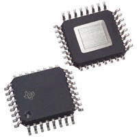
D 9×9 mm PowerPAD Quad Flatpack
APPLICATIONS
D Thermoelectric Cooler (TEC) Driver
D Laser Diode Biasing
VDD
OUT+
OUT+
OUT+
OUT+
PVDD
PVDD
1 µF
1 µF
PVDD
PVDD
10 µF
10 µH
PGND
PWM Input 1
IN+
PGND
PWM Input 2
IN–
PGND
SHUTDOWN
OUT–
PVDD
Shutdown Control
10 µF
10 µH
1 µF
To TEC or Laser
Diode Anode
OUT–
PGND
FAULT0
OUT–
FAULT1
To Fault Monitor
OUT–
PGND
OUT–
PGND
HI-Z
PVDD
AGND (Connect to PowerPAD)
To HI-Z Control
PVDD
OUT+
PVDD
AVDD
10 µF
To TEC or Laser
Diode Cathode
Please be aware that an important notice concerning availability, standard warranty, and use in critical applications of Texas Instruments
semiconductor products and disclaimers thereto appears at the end of this data sheet.
PowerPAD is a trademark of Texas Instruments.
���������� � � !"#$%&' #! ( )*$$+!' &( #" ,*-. )&' #! /&'+0 �$#/*)'(
)#!"#$% '# (,+) " )&' #!( ,+$ '1+ '+$%( #" �+2&( �!('$*%+!'( ('&!/&$/ 3&$$&!'40
�$#/*)' #! ,$#)+(( !5 /#+( !#' !+)+((&$ .4 !).*/+ '+(' !5 #" &.. ,&$&%+'+$(0
Copyright 2002, Texas Instruments Incorporated
�������
www.ti.com
SLOS390A – NOVEMBER 2001– REVISED MAY 2002
This integrated circuit can be damaged by ESD. Texas
Instruments recommends that all integrated circuits be
handled with appropriate precautions. Failure to observe
proper handling and installation procedures can cause damage.
ESD damage can range from subtle performance degradation to
complete device failure. Precision integrated circuits may be more
susceptible to damage because very small parametric changes could
cause the device not to meet its published specifications.
ORDERING INFORMATION
TA
PowerPAD QUAD FLATPACK
(VFP)
DRV592VFP(1)
–40°C to 85°C
(1) This package is available taped and reeled. To order this
packaging option, add an R suffix to the part number (e.g.,
DRV592VFPR).
ABSOLUTE MAXIMUM RATINGS
over operating free-air temperature range unless otherwise noted(1)
Supply voltage, AVDD, PVDD
Input voltage, VI
Output current, IO (FAULT0, FAULT1)
Continuous total power dissipation
DRV591
UNIT
–0.3 to 5.5
V
–0.3 to VDD + 0.3
V
1
mA
See Dissipation Rating Table
Operating free-air temperature range, TA
–40 to 85
°C
Operating junction temperature range, TJ
–40 to 150
°C
Storage temperature range, Tstg
–65 to 165
°C
(1) Stresses beyond those listed under “absolute maximum ratings” may cause permanent damage to the device. These are stress ratings only, and
functional operation of the device at these or any other conditions beyond those indicated under “recommended operating conditions” is not
implied. Exposure to absolute-maximum-rated conditions for extended periods may affect device reliability.
RECOMMENDED OPERATING CONDITIONS
ÑÑÑÑÑÑÑÑÑÑÑÑÑÑÑÑÑÑÑÑÑÑÑÑÑÑÑÑÑ
ÑÑÑ
ÑÑÑ
ÑÑÑÑÑÑÑÑÑÑÑÑÑÑÑ
ÑÑÑÑÑÑÑÑÑÑÑÑÑÑÑ
ÑÑÑÑÑ
ÑÑ
ÑÑÑ
ÑÑÑÑÑÑÑÑÑÑÑÑÑÑÑÑÑÑÑÑÑÑÑÑÑÑÑÑÑ
ÑÑÑÑÑÑÑÑÑÑÑÑÑÑÑ
ÑÑÑÑÑÑÑÑÑÑÑÑÑÑÑÑÑÑÑÑÑÑÑÑÑÑÑÑÑ
ÑÑÑÑÑÑÑÑÑÑÑÑÑÑÑ
ÑÑÑ
Ñ
ÑÑ
ÑÑÑ
Ñ
ÑÑÑÑÑÑÑÑÑÑÑÑÑÑÑÑÑÑÑÑÑÑÑÑÑÑÑÑÑ
ÑÑÑÑÑ
ÑÑÑ
MIN
Supply voltage, AVDD, PVDD
2.8
High-level input voltage, VIH
SHUTDOWN, HI-Z, IN+, IN–
Low-level input voltage, VIL
SHUTDOWN, HI-Z, IN+, IN–
Operating free-air temperature, TA
PACKAGE
ΘJA(1)
(°C/W)
ΘJC
(°C/W)
TA = 25°C
POWER RATING
VFP
29.4
1.2
4.1 W
(1) This data was taken using 2 oz trace and copper pad that is
soldered directly to a JEDEC standard 4-layer 3 in × 3 in PCB.
2
5.5
2
–40
PACKAGE DISSIPATION RATINGS
MAX UNIT
V
V
0.8
V
85
°C
�������
www.ti.com
SLOS390A – NOVEMBER 2001– REVISED MAY 2002
ELECTRICAL CHARACTERISTICS
over operating free-air temperature range unless otherwise noted
PARAMETER
TEST CONDITIONS
MIN
TYP
MAX
VO
Voltage output (measured differentially)
VDD = 5 V
IO = ±1 A, rds(on) = 65 mΩ
IO = ±3 A, rds(on) = 65 mΩ
|IIH|
High-level input current
|IIL|
Low-level input current
VDD = 5.5V,
VDD = 5.5V,
VI = VDD
VI = 0 V
VDD = 5 V,
IO = 4 A
A,
TA = 25°C
High side
25
60
95
Low side
25
65
95
VDD = 3.3 V,
IO = 4 A,
A
TA = 25°C
High side
25
80
140
Low side
25
90
140
rDS(on)
Output on-resistance
on resistance
V
4.61
1
µA
1
µA
mΩ
mΩ
Maximum continuous current output
3
Output resistance in shutdown
UNIT
4.87
SHUTDOWN = 0.8 V
1
Switching frequency
2
0 (dc)
Status flag output pins (FAULT0, FAULT1)
Fault active (open drain output)
Sinking 200 µA
Iq
Q i
Quiescent
t currentt
VDD = 5 V
VDD = 3.3 V
Iq(SD)
Quiescent current in shutdown mode
SHUTDOWN = 0.8 V
A
3.5
1
0.1
N switching
No
it hi
0
0.5
1.5
0
0.3
1
0.01
50
kΩ
MHz
V
mA
A
µA
PIN ASSIGNMENTS
PVDD
PVDD
PVDD
PVDD
OUT+
OUT+
OUT+
OUT+
VFP PACKAGE
(TOP VIEW)
32 31 30 29 28 27 26 25
1
24
2
23
22
3
4
PowerPAD
5
21
20
7
19
18
8
17
6
OUT+
PGND
PGND
PGND
PGND
PGND
PGND
OUT–
9 10 11 12 13 14 15 16
PVDD
PVDD
PVDD
PVDD
OUT–
OUT–
OUT–
OUT–
AVDD
AGND
HI-Z
FAULT1
FAULT0
IN+
IN–
SHUTDOWN
3
�������
www.ti.com
SLOS390A – NOVEMBER 2001– REVISED MAY 2002
Terminal Functions
TERMINAL
NAME
NO.
I/O
DESCRIPTION
AGND
2
AVDD
1
I
Analog power supply
FAULT0
5
O
Fault flag 0, low when active open drain output (see application information)
FAULT1
4
O
Fault flag 1, low when active open drain output (see application information)
HI-Z
3
I
Places both outputs of the H-bridge into a high-impedance state (2 kΩ to ground) when a TTL logic low is
applied to this terminal; normal operation when a TTL logic high is applied.
IN–
7
I
Negative H-bridge input
IN+
6
I
Positive H-bridge input
OUT–
13–17
O
Negative H-bridge output (5 terminals)
OUT+
24–28
O
Positive H-bridge output (5 terminals)
PGND
18–23
PVDD
9–12,
29–32
I
High-current power supply (8 terminals)
8
I
Places the amplifier in shutdown mode when a TTL logic low is applied to this terminal; places the amplifier in
normal operation when a TTL logic high is applied
SHUTDOWN
Analog ground
High-current ground (6 terminals)
FUNCTIONAL BLOCK DIAGRAM
AVDD
AVDD
IN+
IN–
SHUTDOWN
IN+
TTL
Input IN–
Buffer
AGND
PVDD
Gate
Drive
OUT+
PGND
SDZ
PVDD
OUT–
Gate
Drive
HI-Z
PGND
Biases
and
References
Start-Up
Protection
Logic
4
OC
Detect
Thermal
FAULT0
VDDok
FAULT1
�������
www.ti.com
SLOS390A – NOVEMBER 2001– REVISED MAY 2002
TYPICAL CHARACTERISTICS
TABLE OF GRAPHS
FIGURE
Efficiency
rDS(on)
Iq
PSRR
IO
vs Load resistance
2, 3
vs Supply voltage
4
vs Free-air temperature
5
vs Free-air temperature
6
Supply current
vs Switching frequency
7
Power supply rejection ratio
vs Frequency
8, 9
vs Output voltage
10
vs Ambient temperature
11
Drain-source
Drain
source on-state
on state resistance
Maximum output current
TEST SET-UP FOR GRAPHS
The LC output filter used in Figures 2, 3, 8, and 9 is shown below.
L1
OUT+
C1
RL
L2
OUT–
C2
L1, L2 = 10 µH (part number: CDRH104R, manufacturer: Sumida)
C1, C2 = 10 µF (part number: ECJ-4YB1C106K, manufacturer: Panasonic)
Figure 1. LC Output Filter
5
�������
www.ti.com
SLOS390A – NOVEMBER 2001– REVISED MAY 2002
TYPICAL CHARACTERISTICS
EFFICIENCY
vs
LOAD RESISTANCE
EFFICIENCY
vs
LOAD RESISTANCE
100
100
90
90
PO = 2 W
80
70
PO = 0.5 W
60
50
40
50
40
30
20
20
VDD = 5 V
fS = 500 kHz
PO = 0.25 W
60
30
10
VDD = 3.3 V
fS = 500 kHz
10
0
0
1
2
3
4
5
6
7
8
RL – Load Resistance – Ω
9
1
10
Figure 2
IO = 1 A
TA = 25°C
250
Total
150
Low Side
100
High Side
50
0
2.7
3.1
3.5
3.9
4.3
4.7
VDD – Supply Voltage – V
Figure 4
3
4
5
6
7
8
RL – Load Resistance – Ω
9
10
DRAIN-SOURCE ON-STATE RESISTANCE
vs
FREE-AIR TEMPERATURE
rDS(on) – Drain-Source On-State Resistance – mΩ
rDS(on) – Drain-Source On-State Resistance – mΩ
300
200
2
Figure 3
DRAIN-SOURCE ON-STATE RESISTANCE
vs
SUPPLY VOLTAGE
6
PO = 1 W
70
PO = 0.5 W
Efficiency – %
Efficiency – %
80
PO = 1 W
5.1
5.5
300
250
VDD = 5 V
IO = 1 A
VFP Package
200
Total
150
Low Side
100
High Side
50
0
–40
–15
10
35
60
TA – Free-Air Temperature – °C
Figure 5
85
�������
www.ti.com
SLOS390A – NOVEMBER 2001– REVISED MAY 2002
TYPICAL CHARACTERISTICS
SUPPLY CURRENT
vs
SWITCHING FREQUENCY
300
10
VDD = 3.3 V
IO = 1 A
VFP Package
250
No Load
8
Iq – Supply Current – mA
rDS(on) – Drain-Source On-State Resistance – mΩ
DRAIN-SOURCE ON-STATE RESISTANCE
vs
FREE-AIR TEMPERATURE
Total
200
150
Low Side
100
High Side
VDD = 5 V
6
VDD = 3.3 V
4
2
50
0
–40
–15
10
35
60
0
100 200
85
TA – Free-Air Temperature – °C
300 400 500
Figure 6
POWER SUPPLY REJECTION RATIO
vs
FREQUENCY
–20
VDD = 5 V
fS = 500 kHz
RL = 1 Ω
Vripple = 100 mVpp
PSRR – Power Supply Rejection Ratio – dB
PSRR – Power Supply Rejection Ratio – dB
–20
–40
–50
–60
–70
–80
10
700 800 900 1000
Figure 7
POWER SUPPLY REJECTION RATIO
vs
FREQUENCY
–30
600
Switching Frequency – kHz
100
1k
10k
f – Frequency – Hz
Figure 8
100k
–30
VDD = 3.3 V
fS = 500 kHz
RL = 1 Ω
Vripple = 100 mVpp
–40
–50
–60
–70
–80
10
100
1k
10k
f – Frequency – Hz
100k
Figure 9
7
�������
www.ti.com
SLOS390A – NOVEMBER 2001– REVISED MAY 2002
TYPICAL CHARACTERISTICS
MAXIMUM OUTPUT CURRENT
vs
OUTPUT VOLTAGE
MAXIMUM OUTPUT CURRENT
vs
AMBIENT TEMPERATURE
3.5
3.5
I O – Maximum Output Current – A
I O – Maximum Output Current – A
3
TJ = 100°C
2.5
TJ = 85°C
2
TJ = 125°C
1.5
1
VDD = 5 V
TA = 25°C
VFP Package
0.5
0
0
1
2
3
VO – Output Voltage – V
3
2.5
2
1.5
1
0.5
4
TJ ≤ 125°C
VFP Package
0
–40 –30 –20 –10 0 10 20 30 40 50 60 70 80
TA – Ambient Temperature – °C
5
Figure 10
Figure 11
APPLICATION INFORMATION
VDD
OUT+
OUT+
OUT+
OUT+
PVDD
PVDD
1 µF
PVDD
1 µF
PVDD
10 µF
10 µH
AVDD
OUT+
AGND (Connect to PowerPAD)
PGND
PGND
SHUTDOWN
OUT–
PVDD
Shutdown Control
10 µH
1 µF
10 µF
Figure 12. Typical Application Circuit
8
To TEC or Laser
Diode Anode
OUT–
IN–
OUT–
PGND
PWM Input 2
OUT–
IN+
OUT–
PGND
PWM Input 1
PVDD
PGND
FAULT0
To Fault Monitor
PVDD
PGND
PVDD
HI-Z
FAULT1
To HI-Z Control
10 µF
To TEC or Laser
Diode Cathode
�������
www.ti.com
SLOS390A – NOVEMBER 2001– REVISED MAY 2002
APPLICATION INFORMATION
L
DRIVING EXTERNALLY-GENERATED PWM
TO THE DRV592 INPUTS
OUT+
C
The DRV592 may be simply viewed as a full-H-bridge, with
all the gate drive and protection circuitry fully integrated,
but with no internal PWM generator.
TEC
R
L
OUT–
C
The inputs may be driven independently with a PWM
signal ranging from dc to 1 MHz. The HIGH and LOW
levels must be TTL compatible. For example, when a
voltage 2 V or higher is applied to IN+, then OUT+ goes
to VDD. If a voltage 0.8 V or lower is applied, then the
output goes to ground.
Figure 13. LC Output Filter
L
OUT+
or
OUT–
Any PWM modulation scheme may be applied to the
DRV592 inputs.
C
TEC
R
OUTPUT FILTER CONSIDERATIONS
TEC element manufacturers provide electrical
specifications for maximum dc current and maximum
output voltage for each particular element. The maximum
ripple current, however, is typically only recommended to
be less than 10% with no reference to the frequency
components of the current. The maximum temperature
differential across the element, which decreases as ripple
current increases, may be calculated with the following
equation:
(1)
1
DT +
DT max
ǒ1 ) N2Ǔ
Where:
∆T = actual temperature differential
∆Tmax = maximum temperature differential
(specified by manufacturer)
N = ratio of ripple current to dc current
According to this relationship, a 10% ripple current
reduces the maximum temperature differential by 1%. An
LC network may be used to filter the current flowing to the
TEC to reduce the amount of ripple and, more importantly,
protect the rest of the system from any electromagnetic
interference (EMI).
FILTER COMPONENT SELECTION
The LC filter, which may be designed from two different
perspectives, both described below, will help estimate the
overall performance of the system. The filter should be
designed for the worst-case conditions during operation,
which is typically when the differential output is at 50% duty
cycle. The following section serves as a starting point for
the design, and any calculations should be confirmed with
a prototype circuit in the lab.
Any filter should always be placed as close as possible to
the DRV592 to reduce EMI.
Figure 14. LC Half-Circuit Equivalent
LC FILTER IN THE FREQUENCY DOMAIN
The transfer function for a 2nd order low-pass filter
(Figures 13 and 14) is shown in equation (2):
H LP(jw) +
1
ǒ Ǔ
– ww
0
2
(2)
jw
) 1 w )1
Q 0
w0 + 1
ǸLC
Q + quality factor
w + DRV592 switching frequency
The resonant frequency for the filter is typically chosen to
be at least one order of magnitude lower than the switching
frequency. Equation (2) may then be simplified to give the
following magnitude equation (3). These equations
assume the use of the filter in Figure 13.
ŤH LPŤdB
fo +
+ –40 log
ǒǓ
fs
fo
(3)
1
2p ǸLC
f s + 500 kHz (DRV592 switching frequency)
If L=10 µH and C=10 µF, the resonant frequency is
15.9 kHz, which corresponds to –60 dB of attenuation at
the 500 kHz switching frequency. For VDD = 5 V, the
amount of ripple voltage at the TEC element is
approximately 5 mV.
The average TEC element has a resistance of 1.5 Ω, so the
ripple current through the TEC is approximately 3.4 mA. At
the 3-A maximum output current of the DRV592, this
3.4 mA corresponds to 0.011% ripple current, causing less
than 0.0001% reduction of the maximum temperature
differential of the TEC element (see equation 1).
9
�������
www.ti.com
SLOS390A – NOVEMBER 2001– REVISED MAY 2002
LC FILTER IN THE TIME DOMAIN
The ripple current of an inductor may be calculated using
equation (4):
DI +
L
ǒVO–V TECǓDTs
(4)
L
D + duty cycle (0.5 worst case)
POWER SUPPLY DECOUPLING
T s + 1ńfs + 1ń500 kHz
For VO = 5 V, VTEC = 2.5 V, and L = 10 µH, and a switching
frequency of 500 kHz; the inductor ripple current is
250 mA. To calculate how much of that ripple current flows
through the TEC element, however, the properties of the
filter capacitor must be considered.
For relatively small capacitors (less than 22 µF) with very
low equivalent series resistance (ESR, less than 10 mΩ),
such as ceramic capacitors, the following equation (5) may
be used to estimate the ripple voltage on the capacitor due
to the change in charge:
ǒǓ
f
2
DV + p ǒ1–DǓ o
C
2
fs
2
(5)
V
TEC
SHUTDOWN OPERATION
The DRV592 includes a shutdown mode that disables the
outputs and places the device in a low supply current state.
The SHUTDOWN pin may be controlled with a TTL logic
signal. When SHUTDOWN is held high, the device
operates normally. When SHUTDOWN is held low, the
device is placed in shutdown. The SHUTDOWN pin must
not be left floating. If the shutdown feature is unused, the
pin may be connected to VDD.
FAULT REPORTING
f s + DRV592 switching frequency
The DRV592 includes circuitry to sense three faults:
1
2p ǸLC
For L = 10 µH and C = 10 µF, the cutoff frequency, fo, is
15.9 kHz. For worst case duty cycle of 0.5 and
VTEC = 2.5 V, the ripple voltage on the capacitors is
6.2 mV. The ripple current may be calculated by dividing
the ripple voltage by the TEC resistance of 1.5 Ω, resulting
in a ripple current through the TEC element of 4.1 mA.
Note that this is similar to the value calculated using the
frequency domain approach.
For larger capacitors (greater than 22 µF) with relatively
high ESR (greater than 100 mΩ), such as electrolytic
capacitors, the ESR dominates over the chargingdischarging of the capacitor. The following simple equation
(6) may be used to estimate the ripple voltage:
DV
C
+ DIL
R
ESR
(6)
DI L + inductor ripple current
ESR
+ filter capacitor ESR
For a 100 µF electrolytic capacitor, an ESR of 0.1 Ω is
common. If the 10 µH inductor is used, delivering 250 mA
of ripple current to the capacitor (as calculated above),
then the ripple voltage is 25 mV. This is over ten times that
of the 10 µF ceramic capacitor, as ceramic capacitors
typically have negligible ESR.
10
To reduce the effects of high-frequency transients or
spikes, a small ceramic capacitor, typically 0.1 µF to 1 µF,
should be placed as close to each set of PVDD pins of the
DRV592 as possible. For bulk decoupling, a 10 µF to
100 µF tantalum or aluminum electrolytic capacitor should
be placed relatively close to the DRV592.
D + duty cycle
fo +
R
For worst case conditions, the on-resistance of the output
transistors has been ignored to give the maximum
theoretical ripple current. In reality, the voltage drop across
the output transistors decreases the maximum VO as the
output current increases. It can be shown using equation
(4) that this decreases the inductor ripple current, and
therefore the TEC ripple current.
D Overcurrent
D Undervoltage
D Overtemperature
These three fault conditions are decoded via the FAULT1
and FAULT0 terminals. Internally, these are open-drain
outputs, so an external pull-up resistor of 5 kΩ or greater
is required.
Table 1. Fault Indicators
FAULT1
FAULT0
0
0
Overcurrent
0
1
Undervoltage
1
0
Overtemperature
1
1
Normal operation
The over-current fault is reported when the output current
exceeds four amps. As soon as the condition is sensed,
the over-current fault is set and the outputs go into a
high-impedance state for approximately 3 µs to 5 µs
(500 kHz operation). After 3 µs to 5 µs, the outputs are
re-enabled. If the over-current condition has ended, the
fault is cleared and the device resumes normal operation.
If the over-current condition still exists, the above
sequence repeats.
The under-voltage fault is reported when the operating
voltage is reduced below 2.8 V. This fault is not latched, so
as soon as the power-supply recovers, the fault is cleared
�������
www.ti.com
SLOS390A – NOVEMBER 2001– REVISED MAY 2002
and normal operation resumes. During the under-voltage
condition, the outputs are high-impedance to prevent
over-dissipation due to increased rDS(on).
The over-temperature fault is reported when the junction
temperature exceeds 130°C. The device continues
operating normally until the junction temperature reaches
190°C, at which point the IC is disabled to prevent
permanent damage from occurring. The system’s
controller must reduce the power demanded from the
DRV592 once the over-temperature flag is set, or else the
device switches off when it reaches 190°C. This flag is not
latched, once the junction temperature drops below
130°C, the fault is cleared, and normal operation resumes.
POWER DISSIPATION AND MAXIMUM
AMBIENT TEMPERATURE
Though the DRV592 is much more efficient than traditional
linear solutions, the power drop across the on-resistance
of the output transistors does generate some heat in
the package, which may be calculated as shown in
equation (7):
P
DISS
ǒ OUTǓ
+ I
2
PowerPAD ground connection should be made to
AGND, not PGND. Ground planes are not
recommended for AGND or PGND. Wide traces (100
mils) should be used for PGND while narrow traces
(15 mils) should be used for AGND.
2.
Power supply decoupling. A small 0.1-µF to 1-µF
ceramic capacitor should be placed as close to each
set of PVDD pins as possible, connecting from PVDD
to PGND. A 0.1-µF to 1-µF ceramic capacitor should
also be placed close to the AVDD pin, connecting from
AVDD to AGND. A bulk decoupling capacitor of at
least 10 µF, preferably ceramic, should be placed
close to the DRV592, from PVDD to PGND.
3.
Power and output traces. The power and output
traces should be sized to handle the desired
maximum output current. The output traces should be
kept as short as possible to reduce EMI, i.e., the
output filter should be placed as close as possible to
the DRV592 outputs.
4.
PowerPAD.
The DRV592 in the Quad Flatpack
package uses TI’s PowerPAD technology to enhance
the thermal performance. The PowerPAD is
physically connected to the substrate of the DRV592
silicon, which is connected to AGND. The PowerPAD
ground connection should therefore be kept separate
from PGND as described above. The pad underneath
the AGND pin may be connected underneath the
device to the PowerPAD ground connection for ease
of routing. For additional information on PowerPAD
PCB layout, refer to the PowerPAD Thermally
Enhanced Package application note, TI literature
number SLMA002.
5.
Thermal performance.
For proper thermal
performance, the PowerPAD must be soldered down
to a thermal land, as described in the PowerPAD
Thermally Enhanced Package application note, TI
literature number SLMA002. In addition, at high
current levels (greater than 2 A) or high ambient
temperatures (greater than 25°C), an internal plane
may be used for heat sinking. The vias under the
PowerPAD should make a solid connection, and the
plane should not be tied to ground except through the
PowerPAD connection, as described above.
(7)
r
DS(on), total
For example, at the maximum output current of 3 A through
a total on-resistance of 130 mΩ (at TJ = 25°C), the power
dissipated in the package is 1.17 W.
The maximum ambient temperature may be calculated
using equation (8):
ǒ
T A + TJ * θ JA
P
DISS
Ǔ
(8)
PRINTED-CIRCUIT BOARD (PCB) LAYOUT
CONSIDERATIONS
Since the DRV592 is a high-current switching device, a
few guidelines for the layout of the printed-circuit board
(PCB) must be considered:
1.
Grounding.
Analog ground (AGND) and power
ground (PGND) must be kept separated, ideally back
to where the power supply physically connects to the
PCB, minimally back to the bulk decoupling capacitor
(10 µF ceramic minimum). Furthermore, the
11
�PACKAGE OPTION ADDENDUM
www.ti.com
10-Dec-2020
PACKAGING INFORMATION
Orderable Device
Status
(1)
Package Type Package Pins Package
Drawing
Qty
Eco Plan
(2)
Lead finish/
Ball material
MSL Peak Temp
Op Temp (°C)
Device Marking
(3)
(4/5)
(6)
DRV592VFP
ACTIVE
HLQFP
VFP
32
250
RoHS & Green
NIPDAU
Level-2-260C-1 YEAR
-40 to 85
DRV592
(1)
The marketing status values are defined as follows:
ACTIVE: Product device recommended for new designs.
LIFEBUY: TI has announced that the device will be discontinued, and a lifetime-buy period is in effect.
NRND: Not recommended for new designs. Device is in production to support existing customers, but TI does not recommend using this part in a new design.
PREVIEW: Device has been announced but is not in production. Samples may or may not be available.
OBSOLETE: TI has discontinued the production of the device.
(2)
RoHS: TI defines "RoHS" to mean semiconductor products that are compliant with the current EU RoHS requirements for all 10 RoHS substances, including the requirement that RoHS substance
do not exceed 0.1% by weight in homogeneous materials. Where designed to be soldered at high temperatures, "RoHS" products are suitable for use in specified lead-free processes. TI may
reference these types of products as "Pb-Free".
RoHS Exempt: TI defines "RoHS Exempt" to mean products that contain lead but are compliant with EU RoHS pursuant to a specific EU RoHS exemption.
Green: TI defines "Green" to mean the content of Chlorine (Cl) and Bromine (Br) based flame retardants meet JS709B low halogen requirements of


 工商网监
湘ICP备2023018690号
工商网监
湘ICP备2023018690号
