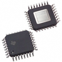
Actual Size
9mm Square
DRV593
DRV594
www.ti.com
SLOS401C – OCTOBER 2002 – REVISED JULY 2010
±3-A HIGH-EFFICIENCY PWM POWER DRIVER
Check for Samples: DRV593, DRV594
FEATURES
1
•
2
•
•
•
•
•
•
•
•
•
DESCRIPTION
Operation Reduces Output Filter Size and Cost
by 50% Compared to DRV591
±3-A Maximum Output Current
Low Supply Voltage Operation: 2.8 V to 5.5 V
High Efficiency Generates Less Heat
Overcurrent and Thermal Protection
Fault Indicators for Overcurrent, Thermal and
Undervoltage Conditions
Two Selectable Switching Frequencies
Internal or External Clock Sync
PWM Scheme Optimized for EMI
9×9 mm PowerPAD™ Quad Flatpack Package
The DRV593 and DRV594 are high-efficiency,
high-current power amplifiers ideal for driving a wide
variety of thermoelectric cooler elements in systems
powered from 2.8 V to 5.5 V. The operation of the
device requires only one inductor and capacitor for
the output filter, saving significant printed-circuit
board area. Pulse-width modulation (PWM) operation
and low output stage on-resistance significantly
decrease power dissipation in the amplifier.
The DRV593 and DRV594 are internally protected
against thermal and current overloads. Logic-level
fault indicators signal when the junction temperature
has reached approximately 128°C to allow for
system-level shutdown before the amplifier's internal
thermal shutdown circuitry activates. The fault
indicators also signal when an overcurrent event has
occurred. If the overcurrent circuitry is tripped, the
devices automatically reset (see application
information section for more details).
APPLICATIONS
•
•
Thermoelectric Cooler (TEC) Driver
Laser Diode Biasing
The PWM switching frequency may be set to 500 kHz
or 100 kHz depending on system requirements. To
eliminate external components, the gain is fixed at
2.3 V/V for the DRV593. For the DRV594, the gain is
fixed at 14.5 V/V.
VDD
PWM
SHUTDOWN
10 µF
H/C
FAULT1
FAULT0
PWM
PVDD
PVDD
PVDD
FREQ
INT/EXT
PGND
1 µF
H/C
Shutdown Control
PGND
IN−
H/C
1 kΩ
PGND
IN+
H/C
1 kΩ
To TEC or Laser
Diode Anode
PGND
DRV593
DRV594
AREF
PVDD
1 µF
PGND
COSC
PVDD
220 pF
PGND
ROSC
PVDD
DC Control
Voltage
10 µH
PWM
AGND (Connect to PowerPAD)
FAULT0
120 kΩ
AVDD
FAULT1
1 µF
PWM
1 µF
10 µF
To TEC or Laser
Diode Cathode
1
2
Please be aware that an important notice concerning availability, standard warranty, and use in critical applications of Texas
Instruments semiconductor products and disclaimers thereto appears at the end of this data sheet.
PowerPAD is a trademark of Texas Instruments.
PRODUCTION DATA information is current as of publication date.
Products conform to specifications per the terms of the Texas
Instruments standard warranty. Production processing does not
necessarily include testing of all parameters.
Copyright © 2002–2010, Texas Instruments Incorporated
�DRV593
DRV594
SLOS401C – OCTOBER 2002 – REVISED JULY 2010
www.ti.com
This integrated circuit can be damaged by ESD. Texas Instruments recommends that all integrated circuits be handled with
appropriate precautions. Failure to observe proper handling and installation procedures can cause damage.
ESD damage can range from subtle performance degradation to complete device failure. Precision integrated circuits may be more
susceptible to damage because very small parametric changes could cause the device not to meet its published specifications.
Table 1. ORDERING INFORMATION (1)
PowerPAD QUAD FLATPACK
(VFP)
TA
DRV593VFP (2)
–40°C to 85°C
(1)
(2)
DRV594VFP (2)
For the most current package and ordering information, see the Package Option Addendum at the end
of this document, or see the TI Web site at www.ti.com
This package is available taped and reeled. To order this packaging option, add an R suffix to the part
number (e.g., DRV593VFPR or DRV594VFPR).
ABSOLUTE MAXIMUM RATINGS
over operating free-air temperature range unless otherwise noted (1)
DRV593, DRV594
AVDD, PVDD
Supply voltage
VI
Input voltage
IO (FAULT0, FAULT1)
Output current
–0.3 V to 5.5 V
–0.3 V to VDD + 0.3 V
1 mA
Continuous total power dissipation
See Dissipation Rating Table
TA
Operating free-air temperature range
–40°C to 85°C
TJ
Operating junction temperature range
–40°C to 150°C
Tstg
Storage temperature range
–65°C to 165°C
(1)
Stresses beyond those listed under absolute maximum ratings may cause permanent damage to the device. These are stress ratings
only, and functional operation of the device at these or any other conditions beyond those indicated under recommended operating
conditions is not implied. Exposure to absolute-maximum-rated conditions for extended periods may affect device reliability.
RECOMMENDED OPERATING CONDITIONS
AVDD, PVDD
Supply voltage
VIH
High-level input voltage
FREQ, INT/EXT, SHUTDOWN, COSC
VIL
Low-level input voltage
FREQ, INT/EXT, SHUTDOWN, COSC
TA
Operating free-air temperature
MIN
MAX
2.8
5.5
2
–40
UNIT
V
V
0.8
V
85
°C
PACKAGE DISSIPATION RATINGS
(1)
2
PACKAGE
qJA (1)
(°C/W)
qJC
(°C/W)
TA=25°C
POWER RATING
VFP
29.4
1.2
4.1 W
This data was taken using 2 oz trace and copper pad that is soldered directly to a JEDEC standard
4-layer 3 in × 3 in PCB.
Submit Documentation Feedback
Copyright © 2002–2010, Texas Instruments Incorporated
Product Folder Link(s): DRV593 DRV594
�DRV593
DRV594
www.ti.com
SLOS401C – OCTOBER 2002 – REVISED JULY 2010
ELECTRICAL CHARACTERISTICS
over operating free-air temperature range unless otherwise noted
PARAMETER
TEST CONDITIONS
MIN
TYP MAX
14
UNIT
|VOO|
Output offset voltage (measured differentially)
VI = VDD/2,
IO = 0 A
100
mV
|IIH|
High-level input current
VDD = 5.5V,
VI = VDD
1
mA
|IIL|
Low-level input current
VDD = 5.5V,
VI = 0 V
1
mA
Vn
Integrated output noise voltage
f =
很抱歉,暂时无法提供与“DRV594VFP”相匹配的价格&库存,您可以联系我们找货
免费人工找货