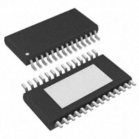
Typical Size
6.4 mm X 9.7 mm
SN65HVS880
www.ti.com............................................................................................................................................... SLAS592C – MARCH 2008 – REVISED NOVEMBER 2008
24 V, EIGHT-CHANNEL DIGITAL-INPUT SERIALIZER
FEATURES
1
• Eight Sensor Inputs
– High Input Voltage up to 30 V
– Selectable Debounce Filters From 0 ms to
3 ms
– Adjustable Current Limits From 0.2 mA to
5.2 mA
– Field Inputs and Supply Lines Protected to
15-kV HBM
• Output Drivers for External Status LEDs
• Cascadable for More Inputs in Multiples of
Eight
2
•
•
•
SPI-Compatible Interface
Regulated 5-V Output for External Digital
Isolator
Over-Temperature and Low-Supply Voltage
Indicator
APPLICATIONS
•
•
•
Sensor Inputs for Industrial Automation and
Process Control
– IEC61131-2 Type 1, 2, or 3 Switches
– EN60947-5-2 Proximity Switches
High Channel Count Digital Input Modules for
PC and PLC Systems
Decentralized I/O Modules
DESCRIPTION
The SN65HVS880 is a 24-V, eight-channel, digital-input serializer for high-channel density digital input modules
of PC and PLC based systems in industrial automation. In combination with galvanic isolators the device
completes the interface between the 24-V sensor outputs of the field-side and the low-voltage controller inputs at
the control-side. Input signals provided by EN60947-5-2 compliant 2- and 3-wire proximity switches are
current-limited and then validated by internal debounce filters. The input switching characteristic is in accordance
with IEC61131-2 for Type 1, 2, and 3 sensor switches.
Upon the application of load and clock signals, input data is latched in parallel into the shift register and
afterwards clocked out serially via a subsequent isolator into a serial PLC input.
Cascading of multiple SN65HVS880 is possible by connecting the serial output of the leading device with the
serial input of the following device, enabling the design of high-channel count input modules. Input status is
indicated via 3-mA constant current LED outputs. An external precision resistor is required to set the internal
reference current. The integrated voltage regulator provides a 5-V output to supply low-power isolators. An
on-chip temperature sensor together with an internal supply voltage monitor provides a chip-okay (CHOK)
indication.
The SN65HVS880 comes in a 28-pin PWP PowerPAD™ package allowing for efficient heat dissipation. The
device is specified for operation at temperatures from –40°C to 85°C.
1
2
Please be aware that an important notice concerning availability, standard warranty, and use in critical applications of Texas
Instruments semiconductor products and disclaimers thereto appears at the end of this data sheet.
PowerPAD is a trademark of Texas Instruments.
PRODUCTION DATA information is current as of publication date.
Products conform to specifications per the terms of the Texas
Instruments standard warranty. Production processing does not
necessarily include testing of all parameters.
Copyright © 2008, Texas Instruments Incorporated
�SN65HVS880
SLAS592C – MARCH 2008 – REVISED NOVEMBER 2008............................................................................................................................................... www.ti.com
Voltage
Regulator
24 V In
Debounce Select
DB0:DB1
Serial Input
5V
8
8
8
SERIALIZER
LED Outputs
RE0:RE7
2
Signal
Conditioning
Field Inputs
IP0:IP7
5 V Out
IREF Adj: RLIM
Field Ground
3
Control Inputs
LD, CE, CLK
Serial Output
DB0
DB1
IP0
RE0
IP1
RE1
IP2
RE2
IP3
RE3
IP4
RE4
RLIM
V24
1
2
3
4
5
6
7
8
9
10
11
12
13
14
28
27
26
25
24
23
22
21
20
19
18
17
16
15
FGND
SIP
LD
CLK
CE
SOP
IP7
RE7
IP6
RE6
IP5
RE5
CHOK
5VOP
FUNCTIONAL BLOCK DIAGRAM
Voltage
Regulator
V24
5VOP
5V
Thermal
Protection
&
Supply
Monitor
CHOK
FGND
RE0
IP0
SIP
Voltage
Sense
IP7
DB1
Current
Sense
&
RE7
DB0
Debounce
Select
Adj. Current
Thresholds
Debounce
Filter
LD
CE
Channel 0
SERIALZER
RLIM
CLK
Channel 7
SOP
2
Submit Documentation Feedback
Copyright © 2008, Texas Instruments Incorporated
Product Folder Link(s): SN65HVS880
�SN65HVS880
www.ti.com............................................................................................................................................... SLAS592C – MARCH 2008 – REVISED NOVEMBER 2008
TERMINAL FUNCTIONS
TERMINAL
PIN NO.
NAME
DESCRIPTION
1, 2
DB0, DB1
3, 5, 7, 9,
11, 18, 20, 22
Debounce select inputs
IPx
Input channel x
4, 6, 8, 10,
12, 17, 19, 21
REx
Return path x (LED drive)
13
RLIM
Current limiting resistor
14
V24
15
5VOP
24 VDC field supply
5 V output to supply low-power isolators
16
CHOK
Chip okay indicator output
23
SOP
Serial data output
24
CE
Clock enable input
25
CLK
Serial clock input
26
LD
Load pulse input
27
SIP
Serial data input
28
FGND
Field ground
Submit Documentation Feedback
Copyright © 2008, Texas Instruments Incorporated
Product Folder Link(s): SN65HVS880
3
�SN65HVS880
SLAS592C – MARCH 2008 – REVISED NOVEMBER 2008............................................................................................................................................... www.ti.com
ABSOLUTE MAXIMUM RATINGS
over operating free-air temperature range (unless otherwise noted)
MIN
MAX
V24
Field power input
V24
–0.3
35
V
VIPx
Field digital inputs
IPx
–0.3
35
V
VID
Voltage at any logic input
DB0, DB1, CLK, SIP, CE, LD
–0.5
6
V
IO
Output current
CHOK, SOP
±8
mA
All pins
±4
IPx,V24
±15
Human-Body Model (1)
VESD
Electrostatic discharge
PTOT
Continuous total power
dissipation
TJ
Junction temperature
(1)
(2)
(3)
UNIT
kV
Charged-Device Model (2)
All pins
±1
kV
Machine Model (3)
All pins
±100
V
170
°C
MAX
UNIT
See Thermal Characteristics table
JEDEC Standard 22, Method A114-A.
JEDEC Standard 22, Method C101
JEDEC Standard 22, Method A115-A
THERMAL CHARACTERISTICS
PARAMETER
θJA
Junction-to-air thermal resistance
θJB
Junction-to-board thermal resistance
θJC
Junction-to-case thermal resistance
PD
Device power dissipation
TEST CONDITIONS
MIN
TYP
High-K thermal resistance
ILOAD = 50 mA, RIN = 0, IPO–IP7 = V24 = 30 V,
RE7 = FGND, fCLK = 100 MHz,
IIP-LIM and ICC = worst case with RLIM = 25 kΩ
35
°C/W
15
°C/W
4.27
°C/W
2591
mW
RECOMMENDED OPERATING CONDITIONS
V24
Field supply voltage
VIPL
Field input low-state input voltage (1)
MIN
TYP
MAX
18
24
30
V
6
V
0
(1)
UNIT
VIPH
Field input high-state input voltage
10
30
V
VIL
Logic low-state input voltage
0
0.8
V
VIH
Logic high-state input voltage
2
5.5
V
RLIM
Current limiter resistor
500
kΩ
fIP
Input data rate (2)
17
0
TJ
TA
(1)
(2)
4
–40
25
1
Mbps
150
°C
85
°C
Field input voltages correspond to an input resistor of RIN = 1.2 kΩ
Maximum data rate corresponds to 0 ms debounce time, (DB0 = open, DB1 = FGND), and RIN = 0 Ω
Submit Documentation Feedback
Copyright © 2008, Texas Instruments Incorporated
Product Folder Link(s): SN65HVS880
�SN65HVS880
www.ti.com............................................................................................................................................... SLAS592C – MARCH 2008 – REVISED NOVEMBER 2008
ELECTRICAL CHARACTERISTICS
all voltages measured against FGND unless otherwise stated, see Figure 12
SYMBOL
PARAMETER
TERMINAL
VTH–(IP)
Low-level device input threshold voltage
VTH+(IP)
High-level device input threshold voltage
VHYS(IP)
Device input hysteresis
VTH–(IN)
Low-level field input threshold voltage
VTH+(IN)
High-level field input threshold voltage
VHYS(IN)
Field input hysteresis
VTH–(V24)
Low-level V24-monitor threshold voltage
VTH+(V24)
High-level V24-monitor threshold voltage
IP0–IP7
TEST CONDITIONS
MIN
TYP
4
4.3
18 V< V24 < 30 V,
RIN = 0 Ω
5.2
measured at
field side of RIN
18 V < V24 < 30 V,
RIN = 1.2 kΩ ± 5%,
RLIM = 25 kΩ
V24
16.8
IP0–IP7
Input current limit
VOL
Logic low-level output voltage
VOH
Logic high-level output voltage
IIL
Logic input leakage current
IRE-on
RE on-state current
ICC(V24)
Supply current
VO(5V)
ILIM(5V)
SOP, CHOK
V
18
V24
Linear regulator output voltage
5VOP
V
1.4
1.83
2.3
kΩ
10 V < VIPx < 30 V,
RLIM = 25 kΩ
3.15
3.6
4
mA
IOL = 20 µA
0.4
IOH = –20 µA
4
RLIM = 25 kΩ,
REX = FGND
2.8
3.15
IP0 to IP7 = V24,
5VOP = open,
REX = FGND,
All logic inputs open
50
µA
3.5
mA
8.7
mA
18 V < V24 < 30 V,
no load
4.5
5
5.5
18 V < V24 < 30 V,
IL = 50 mA
4.5
5
5.5
V
115
5VOP, V24
tDB
Debounce times of input channels
IP0–IP7
tDB-HL
Voltage monitor debounce time after V24 < 15
V (CHOK turns low)
V
V
–50
Linear regulator output current limit
ΔV5/ΔV24 Line regulation
V
3 V < VIPx < 6 V,
RIN = 1.2 kΩ ± 5%,
RLIM = 25 kΩ
DB0, DB1, SIP,
LD, CE, CLK
RE0–RE7
V
V
16.05
0.75
Input resistance
IIP-LIM
V
10
1
15
V
V
8.4
9.4
UNIT
V
5.5
0.9
6
VHYS(V24) V24-monitor hysteresis
RIP
MAX
18 V < V24 < 30 V,
IL = 5 mA
mA
2
DB0 = open,
DB1 = FGND
0
DB0 = FGND,
DB1 = open
1
DB0 = DB1 = open
3
mV/V
ms
1
ms
6
ms
V24, CHOK
tDB-LH
Voltage monitor debounce time after V24 > 18
V (CHOK turns high)
TOVER
Over-temperature indication
150
°C
TSHDN
Shutdown temperature
170
°C
Submit Documentation Feedback
Copyright © 2008, Texas Instruments Incorporated
Product Folder Link(s): SN65HVS880
5
�SN65HVS880
SLAS592C – MARCH 2008 – REVISED NOVEMBER 2008............................................................................................................................................... www.ti.com
TIMING REQUIREMENTS
over operating free-air temperature range (unless otherwise noted)
SYMBOL
PARAMETER
MIN
TYP
MAX
UNIT
tW1
CLK pulse width
See Figure 6
4
ns
tW2
LD pulse width
See Figure 4
6
ns
tSU1
SIP to CLK setup time
See Figure 7
4
ns
tH1
SIP to CLK hold time
See Figure 7
2
ns
tSU2
Falling edge to rising edge (CE to CLK) setup time
See Figure 8
4
ns
tREC
LD to CLK recovery time
See Figure 5
2
fCLK
Clock pulse frequency
See Figure 6
DC
ns
100
MHz
SWITCHING CHARACTERISTICS
over operating free-air temperature range (unless otherwise noted)
SYMBOL
PARAMETER
TEST CONDITIONS
MIN
TYP
MAX
UNIT
tPLH1, tPHL1
CLK to SOP
CL = 15 pF, see Figure 6
10
ns
tPLH2, tPHL2
LD to SOP
CL = 15 pF, see Figure 4
14
ns
tr, tf
Rise and fall times
CL = 15 pF, see Figure 6
5
ns
6
Submit Documentation Feedback
Copyright © 2008, Texas Instruments Incorporated
Product Folder Link(s): SN65HVS880
�SN65HVS880
www.ti.com............................................................................................................................................... SLAS592C – MARCH 2008 – REVISED NOVEMBER 2008
INPUT CHARACTERISTICS
30
RIN = 1.2 kΩ
25
a) IIP-LIM = 2.5 mA ( RLIM = 36.1 kΩ)
b) IIP-LIM = 3.0 mA ( RLIM = 30.1 kΩ)
VIN (V)
a)
b)
c)
c) IIP-LIM = 3.6 mA ( RLIM = 24.9 kΩ)
20
15
10
Off
On
5
Field Input Thresholds
0
0
.
0.5
1.0
1.5
2.0
2.5
3.0
3.5
4.0
IIN (mA)
Figure 1. Typical Input Characteristics
9.6
101.5
V24 = 24 V
VIN = 24 V
9.4
101.0
RIN = 1.2 kΩ
9.2
RLIM = 24.9 kΩ
9.0
100.5
VIN (V)
IIP-LIM/IIP-LIM–25ºC(%)
102.0
100.0
8.8
VTH+(IN)
V24 = 24 V
RIN = 1.2 kΩ
RLIM = 24.9 kΩ
8.6
99.5
8.4
99.0
VTH–(IN)
8.2
98.5
98.0
–45 –35 –25 –15 –5
5
15
25
35
45
55
65
75
85
95
8.0
–45 –35 –25 –15 –5
5
15
25
35
45
55
65
75
85
95
TA (ºC)
TA (ºC)
Figure 2. Typical Current Limiter Variation vs Ambient
Temperature
Figure 3. Typical Limiter Threshold Voltage Variation vs
Ambient Temperature
Submit Documentation Feedback
Copyright © 2008, Texas Instruments Incorporated
Product Folder Link(s): SN65HVS880
7
�SN65HVS880
SLAS592C – MARCH 2008 – REVISED NOVEMBER 2008............................................................................................................................................... www.ti.com
PARAMETER MEASUREMENT INFORMATION
Waveforms
For the complete serial interface timing, refer to Figure 21.
tw2
LD
LD
t REC
t PLH2
tPHL2
CLK
SOP
Figure 4. Parallel – Load Mode
Figure 5. Serial – Shift Mode
valid
1/fCLK
t w1
SIP
CLK
tSU 1
tPLH1
tH1
tPHL1
CLK
SOP
tr
tf
Figure 6. Serial – Shift Mode
Figure 7. Serial – Shift Mode
CLK
t SU2
CE
CLK inhibited
Figure 8. Serial – Shift Clock Inhibit Mode
8
Submit Documentation Feedback
Copyright © 2008, Texas Instruments Incorporated
Product Folder Link(s): SN65HVS880
�SN65HVS880
www.ti.com............................................................................................................................................... SLAS592C – MARCH 2008 – REVISED NOVEMBER 2008
VOLTAGE REGULATOR PERFORMANCE CHARACTERISTICS
5.000
4
ILOAD = 5 mA
4.995
2
TA = 27°C
4.990
ILOAD = 0 mA
4.985
0
VOUT (V)
ΔVOUT (mV)
6
–2
–4
4.980
4.975
–6
4.970
–8
4.965
4.960
–45 –35 –25 –15 –5
–10
0
5
10
15
20
25
30
35
5
15
25 35 45 55 65 75 85 95
TA (°C)
VIN (V)
Figure 9. Line Regulation
Figure 10. Output Voltage vs Ambient Temperature
5.5
5.0
4.5
RLOAD = 100 Ω
VOUT (V)
4.0
3.5
3.0
2.5
2.0
1.5
1.0
0.5
0
0
5
10
15
20
VIN (V)
25
30
35
Figure 11. Output Voltage vs Input Voltage
SIGNAL CONVENTIONS
RIN
IPx
IIN
VTH(IN)
VTH(IP)
SN65HVS880
FGND
Figure 12. On/Off Threshold Voltage Measurements
Submit Documentation Feedback
Copyright © 2008, Texas Instruments Incorporated
Product Folder Link(s): SN65HVS880
9
�SN65HVS880
SLAS592C – MARCH 2008 – REVISED NOVEMBER 2008............................................................................................................................................... www.ti.com
DEVICE INFORMATION
Digital Inputs
1.25 VREF
5V
ILIM Mirror
n = 72
IIN
IPx
ILIM
Limiter
IINmax = ILIM
IREF
RLIM
Figure 13. Digital Input Stage
Each digital input operates as a controlled current sink limiting the input current to a maximum value of ILIM. The
current limit is derived from the reference current via ILIM = n × IREF, and IREF is determined by IREF = VREF/RLIM.
Thus, changing the current limit requires the change of RLIM to a different value via: RLIM = n × VREF/ILIM.
Inserting the actual values for n and VREF gives: RLIM = 90 V / ILIM.
While the device is specified for a current limit of 3.6 mA, (via RLIM = 25 kΩ), it is easy to lower the current limit
to further reduce the power consumption. For example, for a current limit of 2.5 mA simply calculate:
RLIM =
90 V
90 V
=
= 36 kΩ
ILIM
2.5 mA
Debounce Filter
The HVS880 applies a simple analog/digital filtering technique to remove unintended signal transitions due to
contact bounce or other mechanical effects. Any new input (either low or high) must be present for the duration
of the selected debounce time to be latched into the shift register as a valid state.
The logic signal levels at the control inputs, DB0 and DB1 of the internal Debounce-Select logic determine the
different debounce times listed in the following truth table.
Table 1. Debounce Times
DB1
10
DB0
FUNCTION
Open
Open
3 ms delay
Open
FGND
1 ms delay
FGND
Open
0 ms delay
(Filter bypassed)
FGND
FGND
Reserved
Submit Documentation Feedback
Copyright © 2008, Texas Instruments Incorporated
Product Folder Link(s): SN65HVS880
�SN65HVS880
www.ti.com............................................................................................................................................... SLAS592C – MARCH 2008 – REVISED NOVEMBER 2008
5V
IPx
REF
REx
RLIM
FGND
Figure 14. Equivalent Input Diagram
Shift Register
The conversion from parallel input to serial output data is performed by an eight-channel, parallel-in serial-out
shift register. Parallel-in access is provided by the internal inputs, PIP0–PIP7, that are enabled by a low level at
the load input (LD). When clocked, the latched input data shift towards the serial output (SOP). The shift register
also provides a clock-enable function.
Clocking is accomplished by a low-to-high transition of the clock (CLK) input while LD is held high and the clock
enable (CE) input is held low. Parallel loading is inhibited when LD is held high. The parallel inputs to the register
are enabled while LD is low independently of the levels of the CLK, CE, or serial (SIP) inputs.
SIP
D
CLK
CE
Logic
Q
CP
R
D
Q
CP
S
R
D
Q
CP
S
R
D
Q
CP
S
R
D
Q
CP
S
R
D
Q
CP
S
R
D
Q
CP
S
R
D
Q
SOP
CP
S
R
S
LD
PIP 0
PIP 1
PIP 2
PIP 3
PIP 4
PIP 5
PIP 6
PIP 7
Figure 15. Shift Register Logic Structure
Submit Documentation Feedback
Copyright © 2008, Texas Instruments Incorporated
Product Folder Link(s): SN65HVS880
11
�SN65HVS880
SLAS592C – MARCH 2008 – REVISED NOVEMBER 2008............................................................................................................................................... www.ti.com
Table 2. Function Table
INPUTS
(1)
FUNCTION
LD
CLK
CE
L
X
X
Parallel load
H
X
H
No change
H
↑
L
Shift (1)
Shift = content of each internal register shifts towards serial outputs.
Data at SIP is shifted into first register.
Voltage Regulator
The on-chip linear voltage regulator provides a 5 V supply to the internal- and external circuitry, such as digital
isolators, with an output drive capability of 50 mA and a typical current limit of 115 mA. The regulator accepts
input voltages from 30 V down to 10 V. Because the regulator output is intended to supply external digital isolator
circuits proper output voltage decoupling is required. For best results connect a 1 µF and a 0.1 µF ceramic
capacitor as close as possible to the 5VOP-output. For longer traces between the SN65HVS880 and isolators of
the ISO72xx family use additional 0.1 µF and 10 pF capacitors next to the isolator supply pins. Make sure,
however, that the total load capacitance does not exceed 4.7 µF.
For good stability the voltage regulator requires a minimum load current, IL-MIN. Ensure that under any operating
condition the ratio of the minimum load current in mA to the total load capacitance in µF is larger than 1:
IL-MIN 1 mA
>
1 µF
CL
Supply Voltage Monitor
The integrated supply voltage monitor senses the supply voltage of the SN65HVS880 at the V24-pin. If this
voltage drops below 15 V but stays within the regulator’s operating range, i.e., 15 V > V24 > 10 V, the output
CHOK goes low 1 ms later. When the supply voltage returns to 24 V, the CHOK output turns logic high after
6 ms. Should the supply voltage drop below 10 V, the device ceases operation. Upon the supply returning to
above 18 V, the CHOK output turns high again after 6 ms.
18 V
18 V
15 V
15 V
V24
15 V > V24 > 10 V
1 ms
debounce
time starts
10 V
1 ms
debounce
time starts
tDB-HL
tDB-LH
V24 < 10 V
Circuit ceases
operation
tDB-LH
CHOK
Figure 16. CHOK Output Timing as a Function of Supply Voltage Drop at V24
Temperature Sensor
An on-chip temperature sensor monitors the device temperature and signals a fault condition if the device
becomes too hot. A first trip point exists at 150°C. If the junction temperature exceeds this trip point, the sensor
output, being active low, presents a low to the input of the AND gate forcing the CHOK output to go low. If the
junction temperature continues to rise, passing a second trip point at 170°C, all device outputs assume tri-state.
12
Submit Documentation Feedback
Copyright © 2008, Texas Instruments Incorporated
Product Folder Link(s): SN65HVS880
�SN65HVS880
www.ti.com............................................................................................................................................... SLAS592C – MARCH 2008 – REVISED NOVEMBER 2008
Chip Okay (CHOK) Output
The CHOK output is the Boolean AND-function of the two, active-low fault conditions: temperature failure and
supply failure. As such CHOK is a device health indicator, assuming logic high in the absence of any fault
condition. If either one of the two or both fault conditions occur, CHOK becomes logic low.
A special condition occurs, however, when the chip temperature exceeds the second temperature trip point due
to an output short. Then the CHOK output buffer becomes tri-state, thus separating the buffer from the external
circuitry. An internal 100 kΩ pulldown resistor, connecting the CHOK-pin to ground, is used as a “cooling down”
resistor, which continues to provide a logic low level to the external circuitry.
Submit Documentation Feedback
Copyright © 2008, Texas Instruments Incorporated
Product Folder Link(s): SN65HVS880
13
�SN65HVS880
SLAS592C – MARCH 2008 – REVISED NOVEMBER 2008............................................................................................................................................... www.ti.com
APPLICATION INFORMATION
System-Level EMC
The SN65HVS880 must operate reliably in harsh industrial environments. At a system level, the device is tested
according to several international electromagnetic compatibility (EMC) standards.
In addition to the device internal ESD structures, external protection circuitry, such as the one in Figure 17, is
needed to absorb as much energy from burst- and surge-transients as possible.
CC
RS
VSUP = 24 V
DTS
39V Transient Voltage Suppressor: SM15T39CA
DRP
Super Rectifier: BYM10-1000, or
General Purpose rectifier: 1N4007
DZ
33 V – 36 V fast Zener Diode, Z2SMB36
RS
56 Ω, 1/3 W MELF Resistor
RIN
1.2 kΩ, 1/4 W MELF Resistor
CIN
22 nF, 60 V Ceramic Capacitor
CHV
4.7 nF, 2 kV Ceramic Capacitor
CC
n x 220 nF, 60 V Ceramic Capacitors
CB
1 µF - 10 µF, 60 V Ceramic Capacitor
DRP
V 24
CHV
D TS
DZ
CC
CB
CC
SN65HVS880
RIN
INx
IP0 – IP7
CIN
0V
FGND
CHV
FE
Figure 17. Typical EMC Protection Circuitry for Supply and Signal Inputs
Input Channel Switching Characteristics
The input stage of the HVS880 is so designed, that for an input resistor RIN = 1.2 kΩ the trip point for signalling
an ON-condition is at 9.4 V at 3.6 mA. This trip point satisfies the switching requirements of IEC61131-2 Type 1
and Type 3 switches.
Type 2
Type 3
30
30
30
25
25
25
15
10
5
ON
20
VIN (V)
ON
20
VIN (V)
VIN (V)
Type 1
15
10
5
OFF
0
–30
5
10
IIN (mA)
10
5
OFF
0
–3
15
ON
20
15
0
5
10
15
OFF
0
–3
20
25
IIN (mA)
30
0
5
10
IIN (mA)
15
Figure 18. Switching Characteristics for IEC61131-2 Type 1, 2, and 3 Proximity Switches
For a Type 2 switch application, two inputs are connected in parallel. The current limiters then add to a total
maximum current of 7.2 mA. While the return-path (RE-pin), of one input might be used to drive an indicator
LED, the RE-pin of the other input channel should be connected to ground (FGND).
Paralleling input channels reduces the number of available input channels from an octal Type 1 or Type 3 input
to a quad Type 2 input device. Note, that in this configuration output data of an input channel is represented by
two shift register bits.
14
Submit Documentation Feedback
Copyright © 2008, Texas Instruments Incorporated
Product Folder Link(s): SN65HVS880
�SN65HVS880
www.ti.com............................................................................................................................................... SLAS592C – MARCH 2008 – REVISED NOVEMBER 2008
RIN
RIN
IN0
IN0
IP0
IP0
CIN
CIN
RE0
RE0
RIN
RIN
IN1
IP1
IP1
CIN
CIN
RE1
RE1
Figure 19. Paralleling Two Type 1 or Type 3 Inputs Into One Type 2 Input
Digital Interface Timing
The digital interface of the SN65HVS880 is SPI compatible and interfaces, isolated or non-isolated, to a wide
variety of standard micro controllers.
SN65HVS880
IP0
IP7
SERIALIZER
SIP
HOST
CONTROLLER
ISO7241
LD
OUTA
INA
CE
OUTB
INB
CLK
OUTC
INC
SOP
IND
OUTD
LOAD
STE
SCLK
SOMI
Figure 20. Simple Isolation of the Shift Register Interface
Upon a low-level at the load input, LD, the information of the field inputs, IP0 to IP7 is latched into the shift
register. Taking /LD high again blocks the parallel inputs of the shift register from the field inputs. A low-level at
the clock-enable input, CE, enables the clock signal, CLK, to serially shift the data to the serial output, SOP. Data
is clocked at the rising edge of CLK. Thus after eight consecutive clock cycles all field input data have been
clocked out of the shift register and the information of the serial input, SIP, appears at the serial output, SOP.
Submit Documentation Feedback
Copyright © 2008, Texas Instruments Incorporated
Product Folder Link(s): SN65HVS880
15
�SN65HVS880
SLAS592C – MARCH 2008 – REVISED NOVEMBER 2008............................................................................................................................................... www.ti.com
CLK
CE
SIP
high
LD
PIP0–PIP6
PIP7
IP 6
IP7
SOP don’t care
IP 5
IP4
inhibit
IP3
IP2
IP1
IP 0
SIP
Serial shift
Figure 21. Interface Timing for Parallel-Load and Serial-Shift Operation of the Shift Register
Cascading for High Channel Count Input Modules
Designing high-channel count modules require cascading multiple SN65HVS880 devices. Simply connect the
serial output (SOP) of a leading device with the serial input (SIP) of a following device without changing the
processor interface.
HOST
CONTROLLER
ISO7241
4 X SN65HVS880
OUTA
INA
LOAD
OUTB
INB
STE
OUTC
INC
CLK
SCLK
SOMI
SOP
OUTD
IP7
SERIALIZER
IP0
IP7
IP0
SERIALIZER
CE
LD
SIP
SOP
CE
CLK
LD
SIP
SOP
CLK
IP7
SERIALIZER
IP0
IP7
IP0
SERIALIZER
CE
LD
SIP
CLK
SOP
LD
CE
SIP
IND
Figure 22. Cascading Four SN65HVS880 for a 32-Channel Input Module
16
Submit Documentation Feedback
Copyright © 2008, Texas Instruments Incorporated
Product Folder Link(s): SN65HVS880
�SN65HVS880
www.ti.com............................................................................................................................................... SLAS592C – MARCH 2008 – REVISED NOVEMBER 2008
Typical Digital Input Module Application
SM15T39CA
5V
24 V
5 V-ISO
(Logic) 24 V1
SM15T39A
(Sensors) 24 V2
Power
Supply 0 V
4.7 nF
2 kV
Isolated
DC / DC
220 nF
100 V
220 nF
100 V
4.7 nF
2 kV
GND2
GND1
0 V-ISO
4.7 nF
2 kV
56 Ω
MELF
FE
220 nF
100 V
Srew Terminals
BYM10-1000
Z2SMB36
2.2 mF
60 V
1.2 kW
MELF
220 nF
60 V
22 nF
100 V
S0
5VOP
IP0
CE
VCC2
RE0
SIP
EN2
EN1
VCC
LD
OUTA
INA
LOAD
CLK
OUTB
INB
SCLK
ISO7242
VCC1
HOST
CONTROLLER
CHOK
INC
OUTC
INT
RE7
SOP
IND
OUTD
MISO
RLIM
DB0
GND2
GND1
DGND
FGND
DB1
IP7
22 nF
100 V
0.1 mF
V24
1.2 kW
MELF
S7
1 mF
SN65HVS880
24.9 kW
Figure 23. Typical Digital Input Module Application
Submit Documentation Feedback
Copyright © 2008, Texas Instruments Incorporated
Product Folder Link(s): SN65HVS880
17
�PACKAGE OPTION ADDENDUM
www.ti.com
10-Dec-2020
PACKAGING INFORMATION
Orderable Device
Status
(1)
Package Type Package Pins Package
Drawing
Qty
Eco Plan
(2)
Lead finish/
Ball material
MSL Peak Temp
Op Temp (°C)
Device Marking
(3)
(4/5)
(6)
SN65HVS880PWP
ACTIVE
HTSSOP
PWP
28
50
RoHS & Green
NIPDAU
Level-2-260C-1 YEAR
-40 to 85
HVS880
SN65HVS880PWPR
ACTIVE
HTSSOP
PWP
28
2000
RoHS & Green
NIPDAU
Level-2-260C-1 YEAR
-40 to 85
HVS880
(1)
The marketing status values are defined as follows:
ACTIVE: Product device recommended for new designs.
LIFEBUY: TI has announced that the device will be discontinued, and a lifetime-buy period is in effect.
NRND: Not recommended for new designs. Device is in production to support existing customers, but TI does not recommend using this part in a new design.
PREVIEW: Device has been announced but is not in production. Samples may or may not be available.
OBSOLETE: TI has discontinued the production of the device.
(2)
RoHS: TI defines "RoHS" to mean semiconductor products that are compliant with the current EU RoHS requirements for all 10 RoHS substances, including the requirement that RoHS substance
do not exceed 0.1% by weight in homogeneous materials. Where designed to be soldered at high temperatures, "RoHS" products are suitable for use in specified lead-free processes. TI may
reference these types of products as "Pb-Free".
RoHS Exempt: TI defines "RoHS Exempt" to mean products that contain lead but are compliant with EU RoHS pursuant to a specific EU RoHS exemption.
Green: TI defines "Green" to mean the content of Chlorine (Cl) and Bromine (Br) based flame retardants meet JS709B low halogen requirements of


 工商网监
湘ICP备2023018690号
工商网监
湘ICP备2023018690号
