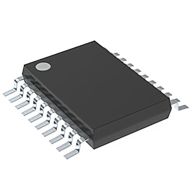
SN74AHC245-Q1
SCLS527B – APRIL 2008 – REVISED NOVEMBER 2022
1 Features
3 Description
•
The SN74AHC245-Q1 octal bus transceiver
is
designed
for
asynchronous
two-way
communication between data buses. The controlfunction implementation minimizes external timing
requirements. This device allows data transmission
from the A bus to the B bus or from the B bus
to the A bus, depending on the logic level at the
direction-control (DIR) input. The output-enable (OE)
input can be used to disable the device so that the
buses effectively are isolated.
•
•
AEC-Q100 qualified for automotive applications:
– Device temperature grade 1: –40°C to +125°C,
TA
– Device HBM ESD Classification Level 2
– Device CDM ESD Classifcation Level C6
Operating range 2 V to 5.5 V VCC
Latch-Up Performance Exceeds 250 mA Per JESD
17
2 Applications
•
•
•
Enable or Disable a Digital Signal
Hold a Signal During Controller Reset
Debounce a Switch
To ensure the high-impedance state during power up
or power down, OE should be tied to VCC through
a pullup resistor; the minimum value of the resistor
is determined by the current-sinking capability of the
driver.
Package Information(1)
PART NUMBER
SN74AHC245-Q1
(1)
(2)
PACKAGE
BODY SIZE (NOM)
PW (TSSOP, 20)
6.50 mm × 4.40 mm
WRKS (WQFN, 20)(2)
4.50 mm × 2.50 mm
For all available packages, see the orderable addendum at
the end of the data sheet.
Preview
1
DIR
19
OE
A1
2
18
B1
To Seven Other Channels
Figure 3-1. Simplified Schematic
An IMPORTANT NOTICE at the end of this data sheet addresses availability, warranty, changes, use in safety-critical applications,
intellectual property matters and other important disclaimers. ADVANCE INFORMATION for preproduction products; subject to change
without notice.
ADVANCE INFORMATION
SN74AHC245-Q1 Automotive Octal Bus Transceivers With 3-State Outputs
�SN74AHC245-Q1
www.ti.com
SCLS527B – APRIL 2008 – REVISED NOVEMBER 2022
Table of Contents
ADVANCE INFORMATION
1 Features............................................................................1
2 Applications..................................................................... 1
3 Description.......................................................................1
4 Revision History.............................................................. 2
5 Pin Configuration and Functions...................................3
6 Specifications.................................................................. 4
6.1 Absolute Maximum Ratings........................................ 4
6.2 ESD Ratings............................................................... 4
6.3 Recommended Operating Conditions.........................4
6.4 Thermal Information....................................................5
6.5 Electrical Characteristics.............................................5
6.6 Switching Characteristics, VCC = 3.3 V ± 0.3 V...........5
6.7 Switching Characteristics, VCC = 5 V ± 0.5 V..............6
6.8 Noise Characteristics.................................................. 6
6.9 Operating Characteristics........................................... 6
6.10 Typical Characteristics.............................................. 7
7 Parameter Measurement Information............................ 8
8 Detailed Description........................................................9
8.1 Overview..................................................................... 9
8.2 Functional Block Diagram........................................... 9
8.3 Feature Description.....................................................9
8.4 Device Functional Modes..........................................10
9 Application and Implementation.................................. 12
9.1 Application Information............................................. 12
9.2 Typical Application.................................................... 12
10 Power Supply Recommendations..............................14
11 Layout........................................................................... 15
11.1 Layout Guidelines................................................... 15
11.2 Layout Example...................................................... 15
12 Device and Documentation Support..........................16
12.1 Receiving Notification of Documentation Updates..16
12.2 Support Resources................................................. 16
12.3 Trademarks............................................................. 16
12.4 Electrostatic Discharge Caution..............................16
12.5 Glossary..................................................................16
13 Mechanical, Packaging, and Orderable
Information.................................................................... 16
4 Revision History
NOTE: Page numbers for previous revisions may differ from page numbers in the current version.
Changes from Revision A (April 2008) to Revision B (November 2022)
Page
• Updated the numbering, formatting, tables, figures, and cross-references throughout the document to reflect
modern data sheet standards............................................................................................................................. 1
• Added Thermal Information table....................................................................................................................... 5
2
Submit Document Feedback
Copyright © 2022 Texas Instruments Incorporated
Product Folder Links: SN74AHC245-Q1
�SN74AHC245-Q1
www.ti.com
SCLS527B – APRIL 2008 – REVISED NOVEMBER 2022
5 Pin Configuration and Functions
1
20
VCC
A1
2
19
OE
A2
3
18
B1
A3
A4
4
17
5
16
B2
B3
A5
6
15
B4
7
8
9
10
14
13
12
11
B5
B6
B7
B8
A6
A7
A8
GND
DIR
1
VCC
20
A1
2
19 OE
A2
3
18 B1
A3
4
17 B2
A4
5
16 B3
PAD
Figure 5-1. SN74AHC245-Q1 PW Package, 20-Pin
TSSOP (Top View)
A5
6
15 B4
A6
7
14 B5
A7
8
13 B6
A8
9
12 B7
10
GND
11
B8
ADVANCE INFORMATION
DIR
Figure 5-2. SN74AHC245-Q1 WRKS Package, 20Pin WQFN (Top View)
Table 5-1. Pin Functions
PIN
NO.
NAME
I/O(1)
DESCRIPTION
1
DIR
I/O
Direction control input (L = B → A, H = A → B)
2
A1
I/O
Channel 1 output/input A
3
A2
I/O
Channel 2 output/input A
4
A3
I/O
Channel 3 output/input A
5
A4
I/O
Channel 4 output/input A
6
A5
I/O
Channel 5 output/input A
7
A6
I/O
Channel 6 output/input A
8
A7
I/O
Channel 7 output/input A
9
A8
I/O
Channel 8 output/input A
10
GND
G
Ground
11
B8
I/O
Channel 8 input/output B
12
B7
I/O
Channel 7 input/output B
13
B6
I/O
Channel 6input/output B
14
B5
I/O
Channel 5input/output B
15
B4
I/O
Channel 4input/output B
16
B
I/O
Channel 3input/output B
17
B2
I/O
Channel 2input/output B
18
B2
I/O
Channel 1input/output B
19
B1
I/O
Output enable, active low
20
VCC
P
Positive supply
Thermal Pad
PAD
-
Thermal Pad(2)
(1)
(2)
I = Input, O = Output, I/O = Input or Output, G = Ground, P = Power.
WRKS Package Only
Submit Document Feedback
Copyright © 2022 Texas Instruments Incorporated
Product Folder Links: SN74AHC245-Q1
3
�SN74AHC245-Q1
www.ti.com
SCLS527B – APRIL 2008 – REVISED NOVEMBER 2022
6 Specifications
6.1 Absolute Maximum Ratings
over operating free-air temperature range (unless otherwise noted) (1)
VCC
Supply voltage range
range(2)
Control inputs
MIN
MAX
–0.5
7
UNIT
V
–0.5
7
V
–0.5
VCC + 0.5
V
VI
Input voltage
VO
I/O, Output voltage range
IIK
Input clamp current
VI < 0
–20
mA
IOK
I/O, Output clamp current
VO < 0 or VO > VCC
±20
mA
IO
Continuous output current
VO = 0 to VCC
±25
mA
±75
mA
Control inputs
Continuous current through VCC or GND
ADVANCE INFORMATION
(1)
(2)
Operation outside the Absolute Maximum Ratings may cause permanent device damage. Absolute Maximum Ratings do not imply
functional operation of the device at these or any other conditions beyond those listed under Recommended Operating Conditions.
If used outside the Recommended Operating Conditions but within the Absolute Maximum Ratings, the device may not be fully
functional, and this may affect device reliability,functionality, performance, and shorten the device lifetime.
The input and output negative-voltage ratings may be exceeded if the input and output current ratings are observed.
6.2 ESD Ratings
VALUE
V(ESD)
(1)
Electrostatic
discharge
Human body model (HBM), per AEC Q100-002 HBM ESD Classification Level
2(1)
±2000
Charged device model (CDM), per AEC Q100-011 CDM ESD Classification
Level C6
±1000
UNIT
V
AEC Q100-002 indicate that HBM stressing shall be in accordance with the ANSI/ESDA/JEDEC JS-001 specification.
6.3 Recommended Operating Conditions
over operating free-air temperature range (unless otherwise noted)(1)
VCC
VIH
Supply voltage
High-level input voltage
MIN
MAX
2
5.5
VCC = 2 V
1.5
VCC = 3 V
2.1
VCC = 5.5 V
Low-level input voltage
V
0.5
VCC = 3 V
0.9
VCC = 5.5 V
V
1.65
VI
Input voltage
OE or DIR
0
5.5
V
VO
Output voltage
A or B
0
VCC
V
–50
µA
IOH
High-level output current
VCC = 2 V
IOL
Low-level output current
∆t/∆v
Input transition rise or fall rate
TA
Operating free-air temperature
(1)
4
V
3.85
VCC = 2 V
VIL
UNIT
VCC = 3.3 V ± 0.3 V
–4
VCC = 5 V ± 0.5 V
–8
VCC = 2 V
50
VCC = 3.3 V ± 0.3 V
4
VCC = 5 V ± 0.5 V
8
VCC = 3.3 V ± 0.3 V
100
VCC = 5 V ± 0.5 V
20
–40
125
mA
µA
mA
ns/V
°C
All unused inputs of the device must be held at VCC or GND to ensure proper device operation. Refer to the TI application report,
Implications of Slow or Floating CMOS Inputs.
Submit Document Feedback
Copyright © 2022 Texas Instruments Incorporated
Product Folder Links: SN74AHC245-Q1
�SN74AHC245-Q1
www.ti.com
SCLS527B – APRIL 2008 – REVISED NOVEMBER 2022
6.4 Thermal Information
THERMAL METRIC(1)
RθJA
(1)
Junction-to-ambient thermal resistance
PW
RKS
20 PINS
20 PINS
83
67.7
UNIT
°C/W
For more information about traditional and new thermal metrics, see the IC Package Thermal Metrics application report.
6.5 Electrical Characteristics
over operating free-air temperature range (unless otherwise noted)
TEST CONDITIONS
VCC
IOH = –50 µA
ICC
1.9
2
1.9
3V
2.9
3
2.9
4.5
4.4
2.58
IOH = –8 mA
4.5 V
3.94
MIN
UNIT
MAX
4.4
V
2.48
3.8
0.1
0.1
3V
0.1
0.1
4.5 V
0.1
0.1
IOL = 4 mA
3V
0.36
0.44
IOL = 8 mA
4.5 V
0.36
0.44
5.5 V
±0.1
±1
0 V to 5.5 V
±0.1
±1
5.5 V
±0.25
±2.5
µA
4
40
µA
10
10
pF
V I = VCC or GND
VI = VCC or GND,
IO = 0
5.5 V
Ci
OE or DIR
VI = VCC or GND
5V
2.5
Cio
A or B inputs
VI = VCC or GND
5V
4
(1)
MAX
2V
VO = VCC or GND,
VI ( OE) = VIL or VIH
IOZ (1)
2V
3V
VOL
OE or DIR
TYP
4.5 V
IOL = 50 µA
II
TA = -40°C to 125°C
MIN
IOH = –4 mA
VOH
A or B inputs
TA = 25°C
ADVANCE INFORMATION
PARAMETER
V
µA
pF
The parameter IOZ includes the input leakage current.
6.6 Switching Characteristics, VCC = 3.3 V ± 0.3 V
over recommended operating free-air temperature range (unless otherwise noted) (see Figure 7-1)
PARAMETER
tPLH
tPHL
tPZH
tPZL
tPHZ
tPLZ
tPLH
tPHL
tPZH
tPZL
tPHZ
tPLZ
FROM
(INPUT)
TO
(OUTPUT)
LOAD
CAPACITANCE
A or B
B or A
CL = 15 pF
OE
A or B
CL = 15 pF
OE
A or B
CL = 15 pF
A or B
B or A
CL = 50 pF
OE
A or B
CL = 50 pF
OE
A or B
CL = 50 pF
TA = 25°C
MIN
TA = -40°C to 125°C
TYP
MAX
MIN
MAX
5.8
8.4
1
10
5.8
8.4
1
10
8.5
13.2
1
15.5
8.5
13.2
1
15.5
8.9
12.5
1
15.5
8.9
12.5
1
15.5
8.3
11.9
1
13.5
8.3
11.9
1
13.5
11
16.7
1
19
11
16.7
1
19
11.5
15.8
1
18
11.5
15.8
1
18
UNIT
ns
ns
ns
ns
ns
ns
Submit Document Feedback
Copyright © 2022 Texas Instruments Incorporated
Product Folder Links: SN74AHC245-Q1
5
�SN74AHC245-Q1
www.ti.com
SCLS527B – APRIL 2008 – REVISED NOVEMBER 2022
6.7 Switching Characteristics, VCC = 5 V ± 0.5 V
over recommended operating free-air temperature range (unless otherwise noted) (see Figure 7-1)
PARAMETER
tPLH
tPHL
tPZH
tPZL
tPHZ
tPLZ
tPLH
ADVANCE INFORMATION
tPHL
tPZH
tPZL
tPHZ
tPLZ
FROM
(INPUT)
TO
(OUTPUT)
LOAD
CAPACITANCE
A or B
B or A
CL = 15 pF
OE
A or B
CL = 15 pF
OE
A or B
CL = 15 pF
A or B
B or A
CL = 50 pF
OE
A or B
CL = 50 pF
OE
A or B
CL = 50 pF
TA = 25°C
MIN
TA = -40°C to 125°C
TYP
MAX
MIN
MAX
4
5.5
1
6.5
4
5.5
1
6.5
5.8
8.5
1
10
5.8
8.5
1
10
5.6
7.8
1
9.2
5.6
7.8
1
9.2
5.5
7.5
1
8.5
5.5
7.5
1
8.5
7.3
10.6
1
12
7.3
10.6
1
12
7
9.7
1
11
7
9.7
1
11
UNIT
ns
ns
ns
ns
ns
ns
6.8 Noise Characteristics
VCC = 5 V, CL = 50 pF, TA = 25°C (1)
PARAMETER
MIN
TYP
MAX
UNIT
VOL(P)
Quiet output, maximum dynamic VOL
0.9
V
VOL(V)
Quiet output, minimum dynamic VOL
–0.9
V
VOH(V)
Quiet output, minimum dynamic VOH
4.3
V
VIH(D)
High-level dynamic input voltage
VIL(D)
Low-level dynamic input voltage
(1)
3.5
V
1.5
V
Characteristics are for surface-mount packages only.
6.9 Operating Characteristics
VCC = 5 V, TA = 25°C
PARAMETER
Cpd
6
Power dissipation capacitance
TEST CONDITIONS
No load
Submit Document Feedback
f = 1 MHz
TYP
14
UNIT
pF
Copyright © 2022 Texas Instruments Incorporated
Product Folder Links: SN74AHC245-Q1
�SN74AHC245-Q1
www.ti.com
SCLS527B – APRIL 2008 – REVISED NOVEMBER 2022
6.10 Typical Characteristics
700
100
25°C
125°C
-40°C
560
70
490
60
420
ICC (µA)
ICC (nA)
80
50
40
210
140
10
70
0.5
1
1.5
2
2.5
3
VCC (V)
3.5
4
4.5
5
0
5.5
Figure 6-1. Supply Current Across Voltage Supply Voltage
0
0.24
3.27
0.21
1.5
2
2.5
VIN (V)
3
3.5
4
4.5
5
0.15
VOL (V)
3.18
3.15
3.12
0.12
0.09
3.09
0.06
3.06
25°C
125°C
-40°C
3.03
25°C
125°C
-40°C
0.03
0
-7
-6
-5
-4
IOH (mA)
-3
-2
-1
0
0
1
2
3
4
IOL (mA)
5
6
7
8
Figure 6-4. Output Voltage vs Current in LOW State; 3.3-V
Supply
Figure 6-3. Output Voltage vs Current in HIGH State; 3.3-V
Supply
5
0.4
4.95
0.35
4.9
0.3
4.85
0.25
VOL (V)
4.8
4.75
4.7
0.2
0.15
4.65
0.1
4.6
25°C
125°C
-40°C
4.55
4.5
-16
1
0.18
3.21
3
-8
0.5
Figure 6-2. Supply Current Across Input Voltage; 5-V Supply
3.3
3.24
VOH (V)
280
20
0
VOH (V)
350
30
0
25°C
125°C
-40°C
630
ADVANCE INFORMATION
90
-14
-12
-10
-8
IOH (mA)
-6
-4
-2
25°C
125°C
-40°C
0.05
0
0
Figure 6-5. Output Voltage vs Current in HIGH State; 5-V Supply
0
2
4
6
8
IOL (mA)
10
12
14
16
Figure 6-6. Output Voltage vs Current in LOW State; 5-V Supply
Submit Document Feedback
Copyright © 2022 Texas Instruments Incorporated
Product Folder Links: SN74AHC245-Q1
7
�SN74AHC245-Q1
www.ti.com
SCLS527B – APRIL 2008 – REVISED NOVEMBER 2022
7 Parameter Measurement Information
RL = 1 kΩ
From Output
Under Test
Test
Point
From Output
Under Test
S1
VCC
Open
TEST
GND
CL
(see Note A)
CL
(see Note A)
S1
tPLH/tPHL
tPLZ/tPZL
tPHZ/tPZH
Open Drain
Open
VCC
GND
VCC
LOAD CIRCUIT FOR
3-STATE AND OPEN-DRAIN OUTPUTS
LOAD CIRCUIT FOR
TOTEM-POLE OUTPUTS
VCC
50% VCC
Timing Input
ADVANCE INFORMATION
tw
tsu
VCC
Input
50% VCC
50% VCC
0V
th
VCC
50% VCC
Data Input
50% VCC
0V
0V
VOLTAGE WAVEFORMS
PULSE DURATION
VOLTAGE WAVEFORMS
SETUP AND HOLD TIMES
VCC
50% VCC
Input
50% VCC
0V
tPLH
In-Phase
Output
tPHL
50% VCC
tPHL
Out-of-Phase
Output
VOH
50% VCC
VOL
Output
Waveform 1
S1 at VCC
(see Note B)
50% VCC
50% VCC
50% VCC
0V
tPLZ
tPZL
≈VCC
50% VCC
Output
Waveform 2
S1 at GND
(see Note B)
VOLTAGE WAVEFORMS
PROPAGATION DELAY TIMES
INVERTING AND NONINVERTING OUTPUTS
VOL + 0.3 V
VOL
tPHZ
tPZH
tPLH
VOH
50% VCC
VOL
VCC
Output
Control
50% VCC
VOH – 0.3 V
VOH
≈0 V
VOLTAGE WAVEFORMS
ENABLE AND DISABLE TIMES
LOW- AND HIGH-LEVEL ENABLING
NOTES: A. CL includes probe and jig capacitance.
B. Waveform 1 is for an output with internal conditions such that the output is low except when disabled by the output control.
Waveform 2 is for an output with internal conditions such that the output is high except when disabled by the output control.
C. All input pulses are supplied by generators having the following characteristics: PRR ≤ 1 MHz, ZO = 50 Ω, tr ≤ 3 ns, tf ≤ 3 ns.
D. The outputs are measured one at a time with one input transition per measurement.
E. All parameters and waveforms are not applicable to all devices.
Figure 7-1. Load Circuit and Voltage Waveforms
8
Submit Document Feedback
Copyright © 2022 Texas Instruments Incorporated
Product Folder Links: SN74AHC245-Q1
�SN74AHC245-Q1
www.ti.com
SCLS527B – APRIL 2008 – REVISED NOVEMBER 2022
8 Detailed Description
8.1 Overview
The SN74AHC245-Q1 is designed for asynchronous two-way communication between data buses. The controlfunction implementation minimizes external timing requirements. The SN74AHC245-Q1 allows data transmission
from the A bus to the B bus or from the B bus to the A bus, depending on the logic level at the direction-control
(DIR) input. The output-enable (OE) input can be used to disable the device so that the buses are effectively
isolated. To ensure the high-impedance state during power up or power down, OE should be tied to VCC through
a pullup resistor; the minimum value of the resistor is determined by the current-sinking capability of the driver.
8.2 Functional Block Diagram
1
ADVANCE INFORMATION
DIR
19
OE
A1
2
18
B1
To Seven Other Channels
8.3 Feature Description
8.3.1 Standard CMOS Inputs
This device includes standard CMOS inputs. Standard CMOS inputs are high impedance and are typically
modeled as a resistor in parallel with the input capacitance given in the Electrical Characteristics. The worst
case resistance is calculated with the maximum input voltage, given in the Absolute Maximum Ratings, and the
maximum input leakage current, given in the Electrical Characteristics, using Ohm's law (R = V ÷ I).
Standard CMOS inputs require that input signals transition between valid logic states quickly, as defined
by the input transition time or rate in the Recommended Operating Conditions table. Failing to meet this
specification will result in excessive power consumption and could cause oscillations. More details can be found
in Implications of Slow or Floating CMOS Inputs.
Do not leave standard CMOS inputs floating at any time during operation. Unused inputs must be terminated at
VCC or GND. If a system will not be actively driving an input at all times, then a pull-up or pull-down resistor can
be added to provide a valid input voltage during these times. The resistor value will depend on multiple factors; a
10-kΩ resistor, however, is recommended and will typically meet all requirements.
8.3.2 Balanced CMOS 3-State Outputs
This device includes balanced CMOS 3-state outputs. Driving high, driving low, and high impedance are the
three states that these outputs can be in. The term balanced indicates that the device can sink and source
similar currents. The drive capability of this device may create fast edges into light loads, so routing and load
conditions should be considered to prevent ringing. Additionally, the outputs of this device can drive larger
currents than the device can sustain without being damaged. It is important for the output power of the device
to be limited to avoid damage due to overcurrent. The electrical and thermal limits defined in the Absolute
Maximum Ratings must be followed at all times.
When placed into the high-impedance mode, the output will neither source nor sink current, with the exception of
minor leakage current as defined in the Electrical Characteristics table. In the high-impedance state, the output
voltage is not controlled by the device and is dependent on external factors. If no other drivers are connected
to the node, then this is known as a floating node and the voltage is unknown. A pull-up or pull-down resistor
Submit Document Feedback
Copyright © 2022 Texas Instruments Incorporated
Product Folder Links: SN74AHC245-Q1
9
�SN74AHC245-Q1
www.ti.com
SCLS527B – APRIL 2008 – REVISED NOVEMBER 2022
can be connected to the output to provide a known voltage at the output while it is in the high-impedance state.
The value of the resistor will depend on multiple factors, including parasitic capacitance and power consumption
limitations. Typically, a 10-kΩ resistor can be used to meet these requirements.
Unused 3-state CMOS outputs should be left disconnected.
8.3.3 Wettable Flanks
This device includes wettable flanks for at least one package. See the Features section on the front page of the
data sheet for which packages include this feature.
Package
Package
Solder
We�able Flank Lead
Standard Lead
ADVANCE INFORMATION
Pad
PCB
Figure 8-1. Simplified Cutaway View of Wettable-Flank QFN Package and Standard QFN Package After
Soldering
Wettable flanks help improve side wetting after soldering, which makes QFN packages easier to inspect with
automatic optical inspection (AOI). As shown in Figure 8-1, a wettable flank can be dimpled or step-cut to
provide additional surface area for solder adhesion which assists in reliably creating a side fillet. See the
mechanical drawing for additional details.
8.3.4 Clamp Diode Structure
As Figure 8-2 shows, the outputs to this device have both positive and negative clamping diodes, and the inputs
to this device have negative clamping diodes only.
CAUTION
Voltages beyond the values specified in the Absolute Maximum Ratings table can cause damage
to the device. The input and output voltage ratings may be exceeded if the input and output clampcurrent ratings are observed.
Device
VCC
+IOK
Input
Output
Logic
-IIK
-IOK
GND
Figure 8-2. Electrical Placement of Clamping Diodes for Each Input and Output
8.4 Device Functional Modes
Function Table lists the functional modes of the SN74AHC245-Q1.
10
Submit Document Feedback
Copyright © 2022 Texas Instruments Incorporated
Product Folder Links: SN74AHC245-Q1
�SN74AHC245-Q1
www.ti.com
SCLS527B – APRIL 2008 – REVISED NOVEMBER 2022
Table 8-1. Function Table
INPUTS(1)
OE
DIR
A
B
L
L
B
Z
L
H
Z
A
H
X
Z
Z
H = High voltage level, L = Low voltage level, X = Don't care
A = Logic value at 'A' input, B = Logic value at 'B' input, Z = High
impedance
ADVANCE INFORMATION
(1)
(2)
OUTPUTS(2)
Submit Document Feedback
Copyright © 2022 Texas Instruments Incorporated
Product Folder Links: SN74AHC245-Q1
11
�SN74AHC245-Q1
www.ti.com
SCLS527B – APRIL 2008 – REVISED NOVEMBER 2022
9 Application and Implementation
Note
Information in the following applications sections is not part of the TI component specification,
and TI does not warrant its accuracy or completeness. TI’s customers are responsible for
determining suitability of components for their purposes, as well as validating and testing their design
implementation to confirm system functionality.
9.1 Application Information
ADVANCE INFORMATION
The SN74AHC245-Q1 can be used to drive signals over relatively long traces or transmission lines. In order to
reduce ringing caused by impedance mismatches between the driver, transmission line, and receiver, a series
damping resistor placed in series with the transmitter’s output can be used. The figure in the Application Curve
section shows the received signal with three separate resistor values. Just a small amount of resistance can
make a significant impact on signal integrity in this type of application.
9.2 Typical Application
Rd
System
Controller
Z0
Rd
Peripheral
L > 12 cm
Transceiver 2
Transceiver 1
Figure 9-1. Application block diagram
9.2.1 Design Requirements
12
Submit Document Feedback
Copyright © 2022 Texas Instruments Incorporated
Product Folder Links: SN74AHC245-Q1
�SN74AHC245-Q1
www.ti.com
SCLS527B – APRIL 2008 – REVISED NOVEMBER 2022
9.2.1.1 Power Considerations
Ensure the desired supply voltage is within the range specified in the Recommended Operating Conditions. The
supply voltage sets the device's electrical characteristics as described in the Electrical Characteristics section.
The ground must be capable of sinking current equal to the total current to be sunk by all outputs of the
SN74AHC245-Q1 plus the maximum supply current, ICC, listed in the Electrical Characteristics, and any
transient current required for switching. The logic device can only sink as much current that can be sunk into
its ground connection. Be sure to not exceed the maximum total current through GND listed in the Absolute
Maximum Ratings.
The SN74AHC245-Q1 can drive a load with a total capacitance less than or equal to 50 pF while still meeting
all of the data sheet specifications. Larger capacitive loads can be applied; however, it is not recommended to
exceed 50 pF.
The SN74AHC245-Q1 can drive a load with total resistance described by RL ≥ VO / IO, with the output voltage
and current defined in the Electrical Characteristics table with VOH and VOL. When outputting in the HIGH state,
the output voltage in the equation is defined as the difference between the measured output voltage and the
supply voltage at the VCC pin.
Total power consumption can be calculated using the information provided in CMOS Power Consumption and
Cpd Calculation.
Thermal increase can be calculated using the information provided in Thermal Characteristics of Standard Linear
and Logic (SLL) Packages and Devices.
CAUTION
The maximum junction temperature, TJ(max) listed in the Absolute Maximum Ratings, is an additional
limitation to prevent damage to the device. Do not violate any values listed in the Absolute Maximum
Ratings. These limits are provided to prevent damage to the device.
9.2.1.2 Input Considerations
Input signals must cross VIL(max) to be considered a logic LOW, and VIH(min) to be considered a logic HIGH. Do
not exceed the maximum input voltage range found in the Absolute Maximum Ratings.
Unused inputs must be terminated to either VCC or ground. The unused inputs can be directly terminated if the
input is completely unused, or they can be connected with a pull-up or pull-down resistor if the input will be used
sometimes, but not always. A pull-up resistor is used for a default state of HIGH, and a pull-down resistor is used
for a default state of LOW. The drive current of the controller, leakage current into the SN74AHC245-Q1 (as
specified in the Electrical Characteristics), and the desired input transition rate limits the resistor size. A 10-kΩ
resistor value is often used due to these factors.
The SN74AHC245-Q1 has CMOS inputs and thus requires fast input transitions to operate correctly, as defined
in the Recommended Operating Conditions table. Slow input transitions can cause oscillations, additional power
consumption, and reduction in device reliability.
Refer to the Feature Description section for additional information regarding the inputs for this device.
Submit Document Feedback
Copyright © 2022 Texas Instruments Incorporated
Product Folder Links: SN74AHC245-Q1
13
ADVANCE INFORMATION
The positive voltage supply must be capable of sourcing current equal to the total current to be sourced
by all outputs of the SN74AHC245-Q1 plus the maximum static supply current, ICC, listed in the Electrical
Characteristics, and any transient current required for switching. The logic device can only source as much
current that is provided by the positive supply source. Be sure to not exceed the maximum total current through
VCC listed in the Absolute Maximum Ratings.
�SN74AHC245-Q1
www.ti.com
SCLS527B – APRIL 2008 – REVISED NOVEMBER 2022
9.2.1.3 Output Considerations
The positive supply voltage is used to produce the output HIGH voltage. Drawing current from the output will
decrease the output voltage as specified by the VOH specification in the Electrical Characteristics. The ground
voltage is used to produce the output LOW voltage. Sinking current into the output will increase the output
voltage as specified by the VOL specification in the Electrical Characteristics.
Push-pull outputs that could be in opposite states, even for a very short time period, should never be connected
directly together. This can cause excessive current and damage to the device.
Two channels within the same device with the same input signals can be connected in parallel for additional
output drive strength.
Unused outputs can be left floating. Do not connect outputs directly to VCC or ground.
Refer to the Feature Description section for additional information regarding the outputs for this device.
ADVANCE INFORMATION
9.2.2 Detailed Design Procedure
1. Add a decoupling capacitor from VCC to GND. The capacitor needs to be placed physically close to the
device and electrically close to both the VCC and GND pins. An example layout is shown in the Layout
section.
2. Ensure the capacitive load at the output is ≤ 50 pF. This is not a hard limit; it will, however, ensure
optimal performance. This can be accomplished by providing short, appropriately sized traces from the
SN74AHC245-Q1 to one or more of the receiving devices.
3. Ensure the resistive load at the output is larger than (VCC / IO(max)) Ω. This will ensure that the maximum
output current from the Absolute Maximum Ratings is not violated. Most CMOS inputs have a resistive load
measured in MΩ; much larger than the minimum calculated previously.
4. Thermal issues are rarely a concern for logic gates; the power consumption and thermal increase, however,
can be calculated using the steps provided in the application report, CMOS Power Consumption and Cpd
Calculation.
9.2.3 Application Curves
5
0
22
50
4
3.3
2
1
0
-1
-2
0
15
30
45
60
Time (ns)
75
90
100
Figure 9-2. Simulated Signal Integrity at the Receiver With Different Damping Resistor (Rd) Values
10 Power Supply Recommendations
The power supply can be any voltage between the minimum and maximum supply voltage rating located in
the Absolute Maximum Ratings section. Each VCC terminal must have a good bypass capacitor to prevent
power disturbance. For devices with a single supply, TI recommends a 0.1-μF capacitor; if there are multiple
VCC terminals, then TI recommends a 0.01-μF or 0.022-μF capacitor for each power terminal. Multiple bypass
capacitors can be paralleled to reject different frequencies of noise. Frequencies of 0.1 μF and 1 μF are
commonly used in parallel. The bypass capacitor must be installed as close as possible to the power terminal for
best results.
14
Submit Document Feedback
Copyright © 2022 Texas Instruments Incorporated
Product Folder Links: SN74AHC245-Q1
�SN74AHC245-Q1
www.ti.com
SCLS527B – APRIL 2008 – REVISED NOVEMBER 2022
11 Layout
11.1 Layout Guidelines
When using multiple bit logic devices, inputs should not float. In many cases, functions or parts of functions of
digital logic devices are unused. Some examples are when only two inputs of a triple-input AND gate are used,
or when only 3 of the 4-buffer gates are used. Such unused input pins must not be left unconnected because
the undefined voltages at the outside connections result in undefined operational states. All unused inputs of
digital logic devices must be connected to a logic high or logic low voltage, as defined by the input voltage
specifications, to prevent them from floating. The logic level that must be applied to any particular unused input
depends on the function of the device. Generally, the inputs are tied to GND or VCC, whichever makes more
sense for the logic function or is more convenient.
VCC
Recommend GND flood fill for
improved signal isolation, noise
reduction, and thermal dissipation
GND
F
DIR
VCC
1
A1
2
20
19
OE
A2
3
18
B1
A3
4
17
B2
A4
5
16
B3
A5
6
15
B4
A6
7
14
B5
A7
8
13
B6
A8
9
10
12
11
B7
GND
GND
B8
ADVANCE INFORMATION
11.2 Layout Example
Bypass capacitor
placed close to the
device
Avoid 90°
corners for
signal lines
Figure 11-1. Example layout for the SN74AHC245-Q1 in the RKS package.
Submit Document Feedback
Copyright © 2022 Texas Instruments Incorporated
Product Folder Links: SN74AHC245-Q1
15
�SN74AHC245-Q1
www.ti.com
SCLS527B – APRIL 2008 – REVISED NOVEMBER 2022
12 Device and Documentation Support
12.1 Receiving Notification of Documentation Updates
To receive notification of documentation updates, navigate to the device product folder on ti.com. Click on
Subscribe to updates to register and receive a weekly digest of any product information that has changed. For
change details, review the revision history included in any revised document.
12.2 Support Resources
TI E2E™ support forums are an engineer's go-to source for fast, verified answers and design help — straight
from the experts. Search existing answers or ask your own question to get the quick design help you need.
Linked content is provided "AS IS" by the respective contributors. They do not constitute TI specifications and do
not necessarily reflect TI's views; see TI's Terms of Use.
ADVANCE INFORMATION
12.3 Trademarks
TI E2E™ is a trademark of Texas Instruments.
All trademarks are the property of their respective owners.
12.4 Electrostatic Discharge Caution
This integrated circuit can be damaged by ESD. Texas Instruments recommends that all integrated circuits be handled
with appropriate precautions. Failure to observe proper handling and installation procedures can cause damage.
ESD damage can range from subtle performance degradation to complete device failure. Precision integrated circuits may
be more susceptible to damage because very small parametric changes could cause the device not to meet its published
specifications.
12.5 Glossary
TI Glossary
This glossary lists and explains terms, acronyms, and definitions.
13 Mechanical, Packaging, and Orderable Information
The following pages include mechanical, packaging, and orderable information. This information is the most
current data available for the designated devices. This data is subject to change without notice and revision of
this document. For browser-based versions of this data sheet, refer to the left-hand navigation.
16
Submit Document Feedback
Copyright © 2022 Texas Instruments Incorporated
Product Folder Links: SN74AHC245-Q1
�PACKAGE OPTION ADDENDUM
www.ti.com
9-Dec-2022
PACKAGING INFORMATION
Orderable Device
Status
(1)
Package Type Package Pins Package
Drawing
Qty
Eco Plan
(2)
Lead finish/
Ball material
MSL Peak Temp
Op Temp (°C)
Device Marking
(3)
Samples
(4/5)
(6)
PN74AHC245QWRKSRQ1
ACTIVE
VQFN
RKS
20
3000
TBD
Call TI
Call TI
-40 to 125
SN74AHC245QPWRG4Q1
ACTIVE
TSSOP
PW
20
2000
RoHS & Green
NIPDAU
Level-1-260C-UNLIM
-40 to 125
AHC245Q1
Samples
SN74AHC245QPWRQ1
ACTIVE
TSSOP
PW
20
2000
RoHS & Green
NIPDAU
Level-1-260C-UNLIM
-40 to 125
AHC245Q1
Samples
Samples
(1)
The marketing status values are defined as follows:
ACTIVE: Product device recommended for new designs.
LIFEBUY: TI has announced that the device will be discontinued, and a lifetime-buy period is in effect.
NRND: Not recommended for new designs. Device is in production to support existing customers, but TI does not recommend using this part in a new design.
PREVIEW: Device has been announced but is not in production. Samples may or may not be available.
OBSOLETE: TI has discontinued the production of the device.
(2)
RoHS: TI defines "RoHS" to mean semiconductor products that are compliant with the current EU RoHS requirements for all 10 RoHS substances, including the requirement that RoHS substance
do not exceed 0.1% by weight in homogeneous materials. Where designed to be soldered at high temperatures, "RoHS" products are suitable for use in specified lead-free processes. TI may
reference these types of products as "Pb-Free".
RoHS Exempt: TI defines "RoHS Exempt" to mean products that contain lead but are compliant with EU RoHS pursuant to a specific EU RoHS exemption.
Green: TI defines "Green" to mean the content of Chlorine (Cl) and Bromine (Br) based flame retardants meet JS709B low halogen requirements of


 工商网监
湘ICP备2023018690号
工商网监
湘ICP备2023018690号
