User's Guide
SLUU373A – July 2009 – Revised June 2014
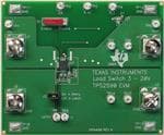
TPS2590 Hot Swap Controller Evaluation Module
This user’s guide describes the setup and operation of the TPS2590 evaluation module.
1
2
3
4
5
6
7
8
9
Contents
Introduction ................................................................................................................... 2
Description .................................................................................................................... 2
2.1
Applications .......................................................................................................... 2
2.2
Features .............................................................................................................. 2
EVM Block Diagram ......................................................................................................... 3
Schematic ..................................................................................................................... 4
Bill of Materials ............................................................................................................... 5
EVM PCB Layout ............................................................................................................ 6
Circuit Description ........................................................................................................... 8
7.1
Test Points ........................................................................................................... 8
7.2
Connectors .......................................................................................................... 8
7.3
Jumpers .............................................................................................................. 8
7.4
Switches ............................................................................................................. 8
EVM Test Setup.............................................................................................................. 9
8.1
Test Equipment ..................................................................................................... 9
8.2
Equipment Supplied ................................................................................................ 9
8.3
Recommended Test Setup ........................................................................................ 9
8.4
Operation ........................................................................................................... 10
Test Results ................................................................................................................. 10
List of Figures
1
TPS2590EVM Block Diagram .............................................................................................. 3
2
TPS2590EVM Schematic ................................................................................................... 4
3
Component Placement (Top View)
4
5
6
7
8
....................................................................................... 6
Board Layout (Top View) ................................................................................................... 6
Board Layout (Bottom View) ............................................................................................... 7
Component Placement (Bottom View) .................................................................................... 7
Equipment Connections..................................................................................................... 9
Example Scope Trace ..................................................................................................... 10
List of Tables
1
TPS2590EVM Bill of Materials ............................................................................................. 5
2
Test Points .................................................................................................................... 8
3
Connectors
4
Jumpers ....................................................................................................................... 8
5
EVM Configurations ......................................................................................................... 9
...................................................................................................................
SLUU373A – July 2009 – Revised June 2014
Submit Documentation Feedback
TPS2590 Hot Swap Controller Evaluation Module
Copyright © 2009–2014, Texas Instruments Incorporated
8
1
�Introduction
1
www.ti.com
Introduction
This user’s guide describes the features of the TPS2590EVM. The TPS2590 schematic, printed-circuit
board (PCB) layout, and bill of materials (BOM) are provided as well as a setup and getting started.
2
Description
The EVM is a 3- to 18-V module using the TPS2590 or TPS2591 hot swap controller with integrated
MOSFET. At power on, the output is power limited to control inrush current and protect the MOSFET. On
an overcurrent condition, the controller interrupts power to the load at high speed and signals load status.
Operating current, fault current and fault timer settings are hardware programmable.
2.1
Applications
Server:
• Plug-in Circuit Boards
• RAID / Disk Drive
Telecom:
• ATCA
• Micro-ATCA
General Hot Plug
2.2
Features
•
•
•
•
•
•
•
•
•
•
•
3- to 20-V operation
Controlled inrush current
Fast circuit breaker control
Hardware programmable
– Operating current
– Fault current
– Fault timer to avoid nuisance tripping
– Latch off or retry. TPS2590 is pin selectable
LED status display
A slide switch controls the ENABLE signal
The area under the TPS2590 is copper pour with vias to the internal ground to take advantage of the
power pad package
On-board transorb for overvoltage input protection
A common diode at the output prevents a negative spike if the load is removed while powered on
Test points available to monitor circuit operation
Design Calculator Tool (http://www.ti.com/product/TPS2590/toolssoftware)
All trademarks are the property of their respective owners.
2
TPS2590 Hot Swap Controller Evaluation Module
Copyright © 2009–2014, Texas Instruments Incorporated
SLUU373A – July 2009 – Revised June 2014
Submit Documentation Feedback
�EVM Block Diagram
www.ti.com
3
EVM Block Diagram
Figure 1 shows the EVM block diagram.
POWER
TPS2590
LOAD+
FAULT
INDICATOR
ENABLE
GND
LOAD-
Figure 1. TPS2590EVM Block Diagram
SLUU373A – July 2009 – Revised June 2014
Submit Documentation Feedback
TPS2590 Hot Swap Controller Evaluation Module
Copyright © 2009–2014, Texas Instruments Incorporated
3
�Schematic
4
www.ti.com
Schematic
Figure 2 shows the EVM schematic.
Figure 2. TPS2590EVM Schematic
4
TPS2590 Hot Swap Controller Evaluation Module
SLUU373A – July 2009 – Revised June 2014
Submit Documentation Feedback
Copyright © 2009–2014, Texas Instruments Incorporated
�Bill of Materials
www.ti.com
5
Bill of Materials
Table 1 lists the BOM for the EVM.
Table 1. TPS2590EVM Bill of Materials
Count
RefDes
Value
Description
Size
Part Number
MFR
2
C1, C3
0.1uF
Capacitor Ceramic, 25V, X7R, 10%
0603
STD
muRata
1
C2
1000pF
Capacitor, Ceramic, 25V, X7R, 20%
0603
STD
muRata
1
C4
.56uF
Capacitor, Ceramic, 10V , X7R, 10%
0805
STD
muRata
1
C5
1uF
Capacitor, Ceramic, 25V, X7R, 20%
1206
STD
muRata
1
C6
.1uF
Capacitor Ceramic, 25V, X7R, 10%
0603
STD
muRata
1
D1
LN1271R
Diode, LED, Red, 20-mA, 0.9-mcd
0.068 x 0.049 inch
LN1271R
Panasonic
1
D2
MMBZ522 Diode, Zener, 4.3V, 350mW
9B
SOT23
MMBZ5229B
Motorola
1
D3
SMAJ18A
Diode, SMT TVS 400W, 1-A, 18V
SMA
SMAJ18A
Diodes
1
D4
MBR130L
SFT1
Diode, Schottky, 1000-mA, 30-V
SOD123
MBR130LSFT1
STD
4
J1, J2, J4,
J5
7693
Screw Terminal
0.310 x 0.310 inch
7693
Keystone
1
J3
PEC02SA Header, 2-pin, 100mil spacing
AN
0.100 inch x 2
PEC02SAAN
Sullins
1
Q1
MMBT390 Bipolar, PNP, 40-V, 200-mA, 225-mW
6LT1
SOT23
MMBT3906LT1
On Semi
1
R1
0
Resistor, Chip, 1/16W, 1%
0603
STD
Vishay
1
R2
499
Resistor, Chip, .5W, 1%
2512
STD
STD
1
R3
10K
Resistor, Chip, 1/16W, 5%
0603
STD
Vishay
1
R4
1K
Resistor, Chip, 1/16W, 1%
0603
STD
Vishay
1
R5
10K
Resistor, Chip, 1/16W, 1%
0603
STD
Vishay
1
R6
20K
Resistor, Chip, 1/16W, 5%
0603
STD
Vishay
1
R7
300
Resistor, Chip, 1/10W, 5%
0805
STD
Vishay
1
R8
40.2K
Resistor, Chip, 1/16W, 1%
0603
STD
Vishay
1
R9
49.9K
Resistor, Chip, 1/16W, 1%
0603
STD
Vishay
1
S1
09-03201- Switch, SPDT, Slide, PC-mount, 500-mA
02
0.400 x 0.100 inch
09-03201-02
EAO
7
TP1, TP2,
TP3, TP4,
TP5, TP6,
TP9
5012
Test Point, White, Thru Hole
0.125 x 0.125 inch
5012
Keystone
4
TP10,
TP11,
TP12,
TP13
GND
Test Point, SM, 0.150 x 0.090
0.185 x 0.135 inch
5016
Keystone
4
TP7, TP8,
TP14,
TP15
Test Point, 0.062 Hole
0.250 inch
5012
Keystone
1
U1
IC, 3V to 20V Integrated FET Load Switch
QFN-16
TPS2590RSA
TI
TPS2590
RSA
SLUU373A – July 2009 – Revised June 2014
Submit Documentation Feedback
TPS2590 Hot Swap Controller Evaluation Module
Copyright © 2009–2014, Texas Instruments Incorporated
5
�EVM PCB Layout
6
www.ti.com
EVM PCB Layout
Figure 3 through Figure 6 illustrate the board outline drawings.
Figure 3. Component Placement (Top View)
Figure 4. Board Layout (Top View)
6
TPS2590 Hot Swap Controller Evaluation Module
Copyright © 2009–2014, Texas Instruments Incorporated
SLUU373A – July 2009 – Revised June 2014
Submit Documentation Feedback
�EVM PCB Layout
www.ti.com
Figure 5. Board Layout (Bottom View)
Figure 6. Component Placement (Bottom View)
SLUU373A – July 2009 – Revised June 2014
Submit Documentation Feedback
TPS2590 Hot Swap Controller Evaluation Module
Copyright © 2009–2014, Texas Instruments Incorporated
7
�Circuit Description
www.ti.com
7
Circuit Description
7.1
Test Points
Table 2 lists the test point descriptions.
Table 2. Test Points
7.2
Name
Description
VIN
Input voltage power supply
4.3 V
4.3-V reference
EN
Enable signal, high true
FLT
Fault signal, low true
LATCH
Latch signal, high true, low for retry
VOUT
Output voltage
CT
Fault timer capacitor
GND
Scope ground test point
GND
Scope ground test point
GND
Scope ground test point
GND
Scope ground test point
Connectors
Table 3 lists the connector descriptions.
Table 3. Connectors
7.3
Connector
Description
J1
Main power input, VIN
J2
Main power ground, GND
J4
Load
J5
Load ground, GND
Jumpers
R1 is used to disconnect the LEDs for test measurement of TPS2590 quiescent current. This 0-Ω resistor
is normally installed.
Table 4 provides the jumper description of jumper J3.
Table 4. Jumpers
7.4
7.4.1
Jumper
Description
J3
TPS2590 Only Off = Latch, On = Retry
Switches
Enable Switch S1
The ENABLE slide switch turns on the hot plug controller to ramp the output voltage. When the switch is
off, the output is off.
7.4.2
Indicators
Red LED indicator for FAULT (FLT).
8
TPS2590 Hot Swap Controller Evaluation Module
Copyright © 2009–2014, Texas Instruments Incorporated
SLUU373A – July 2009 – Revised June 2014
Submit Documentation Feedback
�EVM Test Setup
www.ti.com
8
EVM Test Setup
8.1
Test Equipment
Voltage Source: The input voltage source, VIN is a 20-V variable dc source at 10 A.
Oscilloscope: A digital oscilloscope can be used to monitor the test points.
Current Probe: A current probe is helpful to observe turn-on characteristics of the external load.
Recommended Wire Gague: Power is limited to 5 W; 18-gage wire, minimum, is recommended.
8.2
Equipment Supplied
The TPS2590EVM module configured with TPS2590 is supplied.
Table 5. EVM Configurations
Evaluation Module
Component
HPA490EVM-001
TPS2590
spacer
8.3
Recommended Test Setup
Figure 1 illustrates the equipment connections for power up and testing.
• Connect the positive voltage input power supply to J1 and the negative voltage to GND, J2.
Connectors J1 and J2 can accept #6 ring or spade lugs.
• Connect the RC load at J4 and the load return at J5. The example here uses 220 µF, 15 Ω.
• Scope to current probe to measure the load current.
• Scope the VOUT and EN.
Current
Probe
+
Power
Supply
12V@10A
EN/
Vout
-
Scope
J1
J4
J2
J5
220 µF
15 O
Note:
Connects to Scope
Figure 7. Equipment Connections
SLUU373A – July 2009 – Revised June 2014
Submit Documentation Feedback
TPS2590 Hot Swap Controller Evaluation Module
Copyright © 2009–2014, Texas Instruments Incorporated
9
�EVM Test Setup
8.4
www.ti.com
Operation
Use the following steps for EVM operation:
1. Turn on the power supply.
2. Trigger the scope on EN low-going edge.
3. Slide the EN to the EN position as screened on the circuit board.
9
Test Results
Observe waveforms similar to Figure 8.
• The current to the load is not constant but increases after the initial inrush. Current is low, initially,
because the voltage across the internal MOSFET is initially at its highest level and the controller is
power-limiting the MOSFET.
• Although the current limit, IFLT, is set to 4 A, the start up current never goes above 2.2 A because of the
power limiting. However, 4 A is available to the steady state load when the MOSFET is fully enhanced.
• At the end of the capacitor charge time, the current drops to the dc level powering the resistive part of
the load, about 0.8 A.
Refer to SLUS960 for more details.
Figure 8. Example Scope Trace
10
TPS2590 Hot Swap Controller Evaluation Module
Copyright © 2009–2014, Texas Instruments Incorporated
SLUU373A – July 2009 – Revised June 2014
Submit Documentation Feedback
�Revision History
www.ti.com
Revision History
Changes from Original (July 2009) to A Revision ........................................................................................................... Page
•
•
•
•
•
•
•
•
•
•
Added Design Calculator tool and link to the list of features. .......................................................................
Changed device name in title of Figure 1. .............................................................................................
Changed schematic, Figure 2............................................................................................................
Changed contents of BOM. ..............................................................................................................
Added Component Placement (Bottom View) image. ................................................................................
Changed Board Layout (Top View) image. ............................................................................................
Changed Board Layout (Bottom View) image. ........................................................................................
Added Component Placement (Bottom View) image. ................................................................................
Changed entire content of first paragraph in the Test Points section. .............................................................
Changed R9 to R1 in first paragraph of Jumpers section. ...........................................................................
SLUU373A – July 2009 – Revised June 2014
Submit Documentation Feedback
Revision History
Copyright © 2009–2014, Texas Instruments Incorporated
2
3
4
5
6
6
7
7
8
8
11
�IMPORTANT NOTICE
Texas Instruments Incorporated and its subsidiaries (TI) reserve the right to make corrections, enhancements, improvements and other
changes to its semiconductor products and services per JESD46, latest issue, and to discontinue any product or service per JESD48, latest
issue. Buyers should obtain the latest relevant information before placing orders and should verify that such information is current and
complete. All semiconductor products (also referred to herein as “components”) are sold subject to TI’s terms and conditions of sale
supplied at the time of order acknowledgment.
TI warrants performance of its components to the specifications applicable at the time of sale, in accordance with the warranty in TI’s terms
and conditions of sale of semiconductor products. Testing and other quality control techniques are used to the extent TI deems necessary
to support this warranty. Except where mandated by applicable law, testing of all parameters of each component is not necessarily
performed.
TI assumes no liability for applications assistance or the design of Buyers’ products. Buyers are responsible for their products and
applications using TI components. To minimize the risks associated with Buyers’ products and applications, Buyers should provide
adequate design and operating safeguards.
TI does not warrant or represent that any license, either express or implied, is granted under any patent right, copyright, mask work right, or
other intellectual property right relating to any combination, machine, or process in which TI components or services are used. Information
published by TI regarding third-party products or services does not constitute a license to use such products or services or a warranty or
endorsement thereof. Use of such information may require a license from a third party under the patents or other intellectual property of the
third party, or a license from TI under the patents or other intellectual property of TI.
Reproduction of significant portions of TI information in TI data books or data sheets is permissible only if reproduction is without alteration
and is accompanied by all associated warranties, conditions, limitations, and notices. TI is not responsible or liable for such altered
documentation. Information of third parties may be subject to additional restrictions.
Resale of TI components or services with statements different from or beyond the parameters stated by TI for that component or service
voids all express and any implied warranties for the associated TI component or service and is an unfair and deceptive business practice.
TI is not responsible or liable for any such statements.
Buyer acknowledges and agrees that it is solely responsible for compliance with all legal, regulatory and safety-related requirements
concerning its products, and any use of TI components in its applications, notwithstanding any applications-related information or support
that may be provided by TI. Buyer represents and agrees that it has all the necessary expertise to create and implement safeguards which
anticipate dangerous consequences of failures, monitor failures and their consequences, lessen the likelihood of failures that might cause
harm and take appropriate remedial actions. Buyer will fully indemnify TI and its representatives against any damages arising out of the use
of any TI components in safety-critical applications.
In some cases, TI components may be promoted specifically to facilitate safety-related applications. With such components, TI’s goal is to
help enable customers to design and create their own end-product solutions that meet applicable functional safety standards and
requirements. Nonetheless, such components are subject to these terms.
No TI components are authorized for use in FDA Class III (or similar life-critical medical equipment) unless authorized officers of the parties
have executed a special agreement specifically governing such use.
Only those TI components which TI has specifically designated as military grade or “enhanced plastic” are designed and intended for use in
military/aerospace applications or environments. Buyer acknowledges and agrees that any military or aerospace use of TI components
which have not been so designated is solely at the Buyer's risk, and that Buyer is solely responsible for compliance with all legal and
regulatory requirements in connection with such use.
TI has specifically designated certain components as meeting ISO/TS16949 requirements, mainly for automotive use. In any case of use of
non-designated products, TI will not be responsible for any failure to meet ISO/TS16949.
Products
Applications
Audio
www.ti.com/audio
Automotive and Transportation
www.ti.com/automotive
Amplifiers
amplifier.ti.com
Communications and Telecom
www.ti.com/communications
Data Converters
dataconverter.ti.com
Computers and Peripherals
www.ti.com/computers
DLP® Products
www.dlp.com
Consumer Electronics
www.ti.com/consumer-apps
DSP
dsp.ti.com
Energy and Lighting
www.ti.com/energy
Clocks and Timers
www.ti.com/clocks
Industrial
www.ti.com/industrial
Interface
interface.ti.com
Medical
www.ti.com/medical
Logic
logic.ti.com
Security
www.ti.com/security
Power Mgmt
power.ti.com
Space, Avionics and Defense
www.ti.com/space-avionics-defense
Microcontrollers
microcontroller.ti.com
Video and Imaging
www.ti.com/video
RFID
www.ti-rfid.com
OMAP Applications Processors
www.ti.com/omap
TI E2E Community
e2e.ti.com
Wireless Connectivity
www.ti.com/wirelessconnectivity
Mailing Address: Texas Instruments, Post Office Box 655303, Dallas, Texas 75265
Copyright © 2014, Texas Instruments Incorporated
�


 工商网监
湘ICP备2023018690号
工商网监
湘ICP备2023018690号
