TPS57114C-Q1
SLVSDQ7B – OCTOBER 2016 – REVISED JULY 2021
TPS57114C-Q1 Automotive 2.95-V to 6-V, 4-A 2-MHz Synchronous Buck Converter
1 Features
3 Description
•
•
The TPS57114C-Q1 device is a full-featured 6-V, 4-A,
synchronous step-down current-mode converter with
two integrated MOSFETs.
•
•
•
•
•
•
•
•
•
•
•
Low-voltage, high-density power systems
Point-of-load regulation for high-performance
DSPs, FPGAs, ASICs, and microprocessors
Broadband, networking, and optical
communications infrastructure
TPS57114C-Q1
V(VIN)
VIN
The TPS57114C-Q1 device provides accurate
regulation for a variety of loads with an accurate ±1%
voltage reference (Vref) over temperature.
Efficiency is maximized through the integrated 12-mΩ
MOSFETs and 515-μA typical supply current. Using
the enable pin, shutdown supply current is reduced to
5.5 µA by entering a shutdown mode.
The internal undervoltage lockout setting is 2.45 V,
but programming the threshold with a resistor network
on the enable pin can increase the setting. The slowstart pin controls the output-voltage start-up ramp. An
open-drain power-good signal indicates the output is
within 93% to 107% of the nominal voltage.
Frequency foldback and thermal shutdown protect the
device during an overcurrent condition.
2 Applications
•
•
The TPS57114C-Q1 device enables small designs by
integrating the MOSFETs, implementing current-mode
control to reduce external component count, reducing
inductor size by enabling up to 2-MHz switching
frequency, and minimizing the IC footprint with a small
3-mm × 3-mm thermally enhanced QFN package.
Device Information
PACKAGE(1)
PART NUMBER
TPS57114C-Q1
(1)
WQFN (16)
V(VIN) = 3 V
95
BOOT
V(VIN) = 5 V
90
R4
C(I)
L(O)
EN
85
PH
R5
VO
C(O)
R1
PWRGD
C(SS)
Rt
R3
C1
GND
AGND
Thermal Pad
80
75
70
65
VSENSE
SS/TR
RT/CLK
COMP
BODY SIZE (NOM)
3.00 mm × 3.00 mm
For all available packages, see the orderable addendum at
the end of the data sheet.
100
C(BOOT)
Efficiency (%)
•
Qualified for automotive applications
AEC-Q100 qualified with the following results:
– Device temperature grade 1: –40°C to +125°C
ambient operating temperature range
– Device HBM ESD classification level 2
– Device CDM ESD classification level C4B
Functional Safety-Capable
– Documentation available to aid functional safety
system design
Two 12-mΩ (typical) MOSFETs for high efficiency
at 4-A loads
200-kHz to 2-MHz switching frequency
0.8 V ± 1% voltage reference over temperature
(–40°C to +150°C)
Synchronizes to external clock
Adjustable slow start and sequencing
UV and OV power-good output
–40°C to +150°C operating junction temperature
range
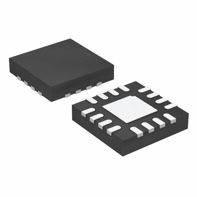
Thermally enhanced 3-mm × 3-mm 16-pin WQFN
Pin-compatible to the TPS54418
Newer product available: TPS62810-Q1, 6-V stepdown converter in 3-mm × 2-mm VQFN package
with wettable flanks
R2
60
55
50
0
1
2
3
4
Output Current (A)
Efficiency Curve
Simplified Schematic
An IMPORTANT NOTICE at the end of this data sheet addresses availability, warranty, changes, use in safety-critical applications,
intellectual property matters and other important disclaimers. PRODUCTION DATA.
�TPS57114C-Q1
www.ti.com
SLVSDQ7B – OCTOBER 2016 – REVISED JULY 2021
Table of Contents
1 Features............................................................................1
2 Applications..................................................................... 1
3 Description.......................................................................1
4 Revision History.............................................................. 2
5 Pin Configuration and Functions...................................3
6 Specifications.................................................................. 4
6.1 Absolute Maximum Ratings........................................ 4
6.2 ESD Ratings............................................................... 4
6.3 Recommended Operating Conditions.........................4
6.4 Thermal Information....................................................5
6.5 Electrical Characteristics.............................................5
6.6 Typical Characteristics................................................ 7
7 Detailed Description...................................................... 11
7.1 Overview................................................................... 11
7.2 Functional Block Diagram......................................... 12
7.3 Feature Description...................................................12
7.4 Device Functional Modes..........................................13
8 Application and Implementation.................................. 22
8.1 Application Information............................................. 22
8.2 Typical Application.................................................... 22
9 Power Supply Recommendations................................31
10 Layout...........................................................................32
10.1 Layout Guidelines................................................... 32
10.2 Layout Example...................................................... 33
11 Device and Documentation Support..........................34
11.1 Device Support........................................................34
11.2 Documentation Support.......................................... 34
11.3 Receiving Notification of Documentation Updates.. 34
11.4 Support Resources................................................. 34
11.5 Trademarks............................................................. 34
11.6 Electrostatic Discharge Caution.............................. 34
11.7 Glossary.................................................................. 34
12 Mechanical, Packaging, and Orderable
Information.................................................................... 34
4 Revision History
NOTE: Page numbers for previous revisions may differ from page numbers in the current version.
Changes from Revision A (July 2021) to Revision B (December 2020)
Page
• Added functional safety bullet to the Features ...................................................................................................1
• Updated the numbering format for tables, figures, and cross-references throughout the document. ................1
• Added TPS62810-Q1 bullet in the Features ......................................................................................................1
Changes from Revision * (October 2016) to Revision A (December 2019)
Page
• First public release..............................................................................................................................................1
2
Submit Document Feedback
Copyright © 2021 Texas Instruments Incorporated
Product Folder Links: TPS57114C-Q1
�TPS57114C-Q1
www.ti.com
SLVSDQ7B – OCTOBER 2016 – REVISED JULY 2021
PH
12
PH
11
BOOT
PWRGD
EN
VIN
5 Pin Configuration and Functions
13
14
15
16
1
VIN
2
VIN
Exposed Thermal Pad
GND
SS/TR
9
4
GND
7
6
5
AGND
8
VSENSE
3
COMP
10
RT/CLK
PH
Figure 5-1. 16-Pin WQFN With Exposed Thermal Pad RTE Package (Bottom View)
Table 5-1. Pin Functions
PIN
I/O
DESCRIPTION
NAME
NO.
AGND
5
—
Connect analog ground electrically to GND close to the device.
BOOT
13
O
The device requires a bootstrap capacitor between BOOT and PH. Having the voltage on this capacitor
below the minimum required by the BOOT UVLO forces the output to switch off until the capacitor
recharges.
COMP
7
O
Error amplifier output, and input to the output-switch current comparator. Connect frequencycompensation components to this pin.
EN
15
I
Enable pin, internal pullup-current source. Pull below 1.2 V to disable. Float to enable. An alternative use
of this pin can be to set the on-off threshold (adjust UVLO) with two additional resistors.
GND
3
4
—
Power ground. Electrically connect this pin directly to the thermal pad under the device.
O
The source of the internal high-side power MOSFET, and drain of the internal low-side (synchronous)
rectifier MOSFET
10
PH
11
12
PWRGD
14
O
An open-drain output; asserts low if output voltage is low because of thermal shutdown, overcurrent,
overvoltage, undervoltage, or EN shutdown.
RT/CLK
8
I
Resistor-timing or external-clock input pin
SS/TR
9
I
Slow start and tracking. An external capacitor connected to this pin sets the output-voltage rise time.
Another use of this pin is for tracking.
I
Input supply voltage: 2.95 V to 6 V
I
Inverting node of the transconductance (gm) error amplifier
1
VIN
2
16
VSENSE
Thermal pad
6
—
Connect the GND pin to the exposed thermal pad for proper operation. Connect this thermal pad to any
internal PCB ground plane using multiple vias for good thermal performance.
Submit Document Feedback
Copyright © 2021 Texas Instruments Incorporated
Product Folder Links: TPS57114C-Q1
3
�TPS57114C-Q1
www.ti.com
SLVSDQ7B – OCTOBER 2016 – REVISED JULY 2021
6 Specifications
6.1 Absolute Maximum Ratings
Input voltage
Output voltage
MIN(1)
MAX(1)
VIN
–0.3
7
EN
–0.3
7
BOOT
–0.3
PH + 7
VSENSE
–0.3
3
COMP
–0.3
3
PWRGD
–0.3
7
SS/TR
–0.3
3
RT/CLK
–0.3
7
BOOT-PH
–0.3
7
PH
–0.6
7
–2
10
PH 10-ns transient
Source current
Sink current
UNIT
V
V
EN
100
µA
RT/CLK
100
µA
COMP
100
µA
PWRGD
10
mA
100
µA
150
°C
SS/TR
Temperature, TJ
–40
Storage temperature, Tstg
(1)
Stresses beyond those listed under Absolute Maximum Ratings may cause permanent damage to the device. These are stress
ratings only, which do not imply functional operation of the device at these or any other conditions beyond those indicated under
Recommended Operating Conditions. Exposure to absolute-maximum-rated conditions for extended periods may affect device
reliability.
6.2 ESD Ratings
VALUE
Human-body model (HBM), per AEC
V(ESD)
(1)
Electrostatic
discharge
Q100-002(1)
Charged-device model (CDM), per AEC
Q100-011
UNIT
±2000
All pins
±500
Corner pins (1, 16, 4, 5, 8, 9, 12, and 13)
±750
V
AEC Q100-002 indicates that HBM stressing shall be in accordance with the ANSI/ESDA/JEDEC JS-001 specification.
6.3 Recommended Operating Conditions
over operating free-air temperature range (unless otherwise noted)
MIN
4
NOM
MAX
UNIT
V(VIN)
Input voltage
2.95
6
V
TA
Operating ambient temperature
–40
125
°C
Submit Document Feedback
Copyright © 2021 Texas Instruments Incorporated
Product Folder Links: TPS57114C-Q1
�TPS57114C-Q1
www.ti.com
SLVSDQ7B – OCTOBER 2016 – REVISED JULY 2021
6.4 Thermal Information
TPS57114C-Q1
THERMAL
METRIC(1)
UNIT
RTE (WQFN)
16 PINS
RθJA
Junction-to-ambient thermal resistance
43.8
°C/W
RθJC(top)
Junction-to-case(top) thermal resistance
46.1
°C/W
RθJB
Junction-to-board thermal resistance
15.5
°C/W
ψJT
Junction-to-top characterization parameter
0.7
°C/W
ψJB
Junction-to-board characterization parameter
15.5
°C/W
3.8
°C/W
RθJC(bottom) Junction-to-case(bottom) thermal resistance
(1)
For more information about traditional and new thermal metrics, see the Semiconductor and IC Package Thermal Metrics application
report (SPRA953).
6.5 Electrical Characteristics
TJ = –40°C to 150°C, V(VIN) = 2.95 to 6 V (unless otherwise noted)
DESCRIPTION
CONDITIONS
MIN
TYP
MAX
UNIT
VIN UVLO start
2.28
2.5
V
VIN UVLO stop
2.45
2.6
V
SUPPLY VOLTAGE (VIN PIN)
Internal undervoltage-lockout threshold
Shutdown supply current
V(EN) = 0 V, 25°C, 2.95 V ≤ V(VIN) ≤ 6 V
5.5
15
µA
Quiescent current – I(q)
V(VSENSE) = 0.9 V, V(VIN) = 5 V, 25°C, Rt = 400 kΩ
515
750
µA
Rising
1.25
Falling
1.18
Enable threshold + 50 mV
–3.2
Enable threshold – 50 mV
–1.65
ENABLE AND UVLO (EN PIN)
Enable threshold
Input current
V
µA
VOLTAGE REFERENCE (VSENSE PIN)
Voltage reference
2.95 V ≤ V(VIN) ≤ 6 V, –40°C < TJ < 150°C
0.792
0.8
0.808
BOOT-PH = 5 V
12
30
BOOT-PH = 2.95 V
16
30
V(VIN) = 5 V
13
30
V(VIN) = 2.95 V
17
30
V
MOSFET
High-side switch resistance
Low-side switch resistance
mΩ
mΩ
ERROR AMPLIFIER
Input current
2
nA
Error-amplifier transconductance (gm)
–2 µA < I(COMP) < 2 µA, V(COMP) = 1 V
245
µS
Error-amplifier transconductance (gm) during
slow start
–2 µA < I(COMP) < 2 µA, V(COMP) = 1 V,
V(VSENSE) = 0.4 V
79
µS
Error-amplifier source and sink
V(COMP) = 1 V, 100-mV overdrive
±20
µA
25
S
COMP to high-side FET current gm
CURRENT LIMIT
Current-limit threshold
V(VIN) = 2.95 V, 25°C
2 ´ DI O
f (SW ) ´ DVO
(26)
where
•
•
•
ΔIO is the change in output current
f(SW) is the regulator switching frequency
ΔVO is the allowable change in the output voltage
C(OUT) >
1
1
´
V
8 ´ f (SW )
O(ripple)
I(ripple)
(27)
where
•
•
•
f(SW) is the switching frequency
VO(ripple) is the maximum allowable output voltage ripple
I(ripple) is the inductor ripple current.
Equation 28 calculates the maximum ESR an output capacitor can have to meet the output-voltage ripple
specification. Equation 28 indicates the ESR should be less than 55 mΩ. In this case, the ESR of the ceramic
capacitor is much less than 55 mΩ.
Factoring in additional capacitance deratings for aging, temperature, and dc bias increases this minimum value.
This example uses two 22-µF, 10-V X5R ceramic capacitors with 3 mΩ of ESR.
Capacitors generally have limits to the amount of ripple current they can handle without failing or producing
excess heat. Select an output capacitor that can support the inductor ripple current. Some capacitor data sheets
specify the root-mean-square (rms) value of the maximum ripple current. Use Equation 29 to calculate the rms
ripple current that the output capacitor must support. For this application, Equation 29 yields 333 mA.
R (ESR) <
I(Co,rms) =
24
VO(ripple)
I(ripple)
(28)
VO ´ (VI(max) - VO )
12 ´ VI(max) ´ L1 ´ f (SW )
(29)
Submit Document Feedback
Copyright © 2021 Texas Instruments Incorporated
Product Folder Links: TPS57114C-Q1
�TPS57114C-Q1
www.ti.com
SLVSDQ7B – OCTOBER 2016 – REVISED JULY 2021
8.2.2.4 Input Capacitor
The TPS57114C-Q1 device requires a high-quality ceramic, type X5R or X7R, input decoupling capacitor with
at least 4.7 µF of effective capacitance, and in some applications a bulk capacitance. The effective capacitance
includes any dc-bias effects. The voltage rating of the input capacitor must be greater than the maximum input
voltage. The capacitor must also have a ripple-current rating greater than the maximum input-current ripple of
the TPS57114C-Q1 device. Calculate the input ripple current using Equation 30.
The value of a ceramic capacitor varies significantly over temperature and the amount of dc bias applied to
the capacitor. One can minimize the capacitance variations due to temperature by selecting a dielectric material
that is stable over temperature. The dielectrics usually selected for power regulator capacitors are X5R and
X7R ceramic because they have a high capacitance-to-volume ratio and are fairly stable over temperature. Also
select the output capacitor with the dc bias taken into account. The capacitance value of a capacitor decreases
as the dc bias across that capacitor increases.
This example design requires a ceramic capacitor with at least a 10-V voltage rating to support the maximum
input voltage. The selections for this example are one 10-µF and one 0.1-µF 10-V capacitor in parallel. The
input capacitance value determines the input ripple voltage of the regulator. Calculate the input voltage ripple
using Equation 31. Using the design example values, IO(max) = 4 A, C(IN) = 10 µF, and f(SW) = 1 MHz, yields an
input-voltage ripple of 100 mV and an rms input-ripple current of 1.96 A.
I(Ci,rms) = I O ´
DVI =
VO
VI(min)
´
(VI(min) - VO )
VI(min)
(30)
I O(max) ´ 0.25
C(IN) ´ f (SW )
(31)
8.2.2.5 Slow-Start Capacitor
The slow-start capacitor determines the minimum amount of time it takes for the output voltage to reach its
nominal programmed value during power up. Slow start is useful if a load requires a controlled rate of voltage
slew. Another use for slow start is if the output capacitance is large and would require large amounts of current
to charge the capacitor quickly to the output-voltage level. The large currents necessary to charge the capacitor
may make the TPS57114C-Q1 device reach the current limit, or excessive current draw from the input power
supply may cause the input voltage rail to sag. Limiting the output-voltage slew rate solves both of these
problems.
Calculate the slow-start capacitor value using Equation 32. For the example circuit, the slow-start time is not too
critical because the output capacitor value is 44 µF, which does not require much current to charge to 1.8 V. The
example circuit has the slow-start time set to an arbitrary value of 4 ms, which requires a 10-nF capacitor. In the
TPS57114C-Q1 device, I(SS/TR) is 2.2 µA and Vref is 0.8 V.
C(SS) (nF) =
t (SS) (ms) ´ I(SS/TR) (mA)
Vref (V)
(32)
8.2.2.6 Bootstrap Capacitor Selection
Connect a 0.1-µF ceramic capacitor between the BOOT and PH pins for proper operation. TI recommends using
a ceramic capacitor with X5R or better-grade dielectric. The capacitor should have a 10-V or higher voltage
rating.
8.2.2.7 Output-Voltage And Feedback-Resistor Selection
For the example design, the selection for R6 is 100 kΩ. Using Equation 33, calculate R7 as 80 kΩ. The nearest
standard 1% resistor is 80.5 kΩ.
Submit Document Feedback
Copyright © 2021 Texas Instruments Incorporated
Product Folder Links: TPS57114C-Q1
25
�TPS57114C-Q1
www.ti.com
SLVSDQ7B – OCTOBER 2016 – REVISED JULY 2021
R7 =
Vref
´ R6
VO - Vref
(33)
Due to the internal design of the TPS57114C-Q1 device, there is a minimum output voltage limit for any given
input voltage. The output voltage can never be lower than the internal voltage reference of 0.8 V. Above 0.8 V,
an output voltage limit may exist due to the minimum controllable on-time. In this case, Equation 34 gives the
minimum output voltage
(
)
(
VO(min) = t (ONmin) ´ f(SWmax) ´ VI(max) - I O(min) ´ 2 ´ rDS(on) - I O(min) ´ R (L) + rDS(on)
)
(34)
where
•
•
•
•
•
•
•
VO(min) = minimum achievable output voltage
t(ONmin) = minimum controllable on-time (65 ns, typical; 120 ns, no load)
f(SWmax) = maximum switching frequency, including tolerance
VI(max) = maximum input voltage
IO(min) = minimum load current
rDS(on) = minimum high-side MOSFET on-resistance (15 mΩ–19 mΩ)
R(L) = series resistance of output inductor
There is also a maximum achievable output voltage, which is limited by the minimum off-time. Equation 35 gives
the maximum output voltage.
(
) (
)
(
VO(max) = 1 - t (OFFmax) ´ f (SWmax) ´ VI(min) - I O(max) ´ 2 ´ rDS(on) - I O(max) ´ R (L) + rDS(on)
)
(35)
where
•
•
•
•
•
•
•
VO(max) = maximum achievable output voltage
t(OFFmax) = maximum off-time (60 ns, typical)
f(SWmax) = maximum switching frequency, including tolerance
VI(min) = minimum input voltage
IO(max) = maximum load current
rDS(on) = maximum high-side MOSFET on-resistance (19 mΩ–30 mΩ)
R(L) = series resistance of output inductor
8.2.2.8 Compensation
There are several industry techniques used to compensate dc-dc regulators. The method presented here is easy
to calculate and yields high phase margins. For most conditions, the regulator has a phase margin between 60
and 90 degrees. The method presented here ignores the effects of the slope compensation that is internal to the
TPS57114C-Q1 device. Because of ignoring the slope compensation, the actual crossover frequency is usually
lower than the crossover frequency used in the calculations. Use SwitcherPro software for a more-accurate
design.
To get started, calculate the modulator pole, f(p,mod), and the ESR zero, f(z, mod), using Equation 36 and Equation
37. For C(OUT), derating the capacitor is not necessary, as the 1.8-V output is a small percentage of the 10-V
capacitor rating. If the output is a high percentage of the capacitor rating, use the manufacturer information for
the capacitor to derate the capacitor value. Use Equation 38 and Equation 39 to estimate a starting point for the
crossover frequency, f(c). For the example design, f(p,mod) is 6.03 kHz and f(z,mod) is 1210 kHz. Equation 38 is the
geometric mean of the modulator pole and the ESR zero and Equation 39 is the mean of the modulator pole
and the switching frequency. Equation 38 yields 85.3 kHz and Equation 39 gives 54.9 kHz. Use the lower value
of Equation 38 or Equation 39 as the approximate crossover frequency. For this example, f(c) is 56 kHz. Next,
calculate the compensation components. Use a resistor in series with a capacitor to create a compensating zero.
A capacitor in parallel with these two components forms the compensating pole (if needed).
26
Submit Document Feedback
Copyright © 2021 Texas Instruments Incorporated
Product Folder Links: TPS57114C-Q1
�TPS57114C-Q1
www.ti.com
SLVSDQ7B – OCTOBER 2016 – REVISED JULY 2021
f (p,mod) =
f (z,mod) =
I O(max)
2p ´ VO ´ C(OUT)
(36)
1
2p ´ R (ESR) ´ C(OUT)
f (c) =
f (p,mod) ´ f (z,mod)
f (c) =
f (p,mod) ´
(37)
(38)
f (SW)
2
(39)
The compensation design takes the following steps:
1. Set up the anticipated crossover frequency. Use Equation 40 to calculate the resistor value for the
compensation network. In this example, the anticipated crossover frequency (f(c)) is 56 kHz. The powerstage gain (gm(ps)) is 25 S, and the error-amplifier gain (gm(ea)) is 245 µS.
R3 =
2p ´ f (c) ´ VO ´ C(OUT)
g m(ea) ´ Vref ´ g m(ps)
(40)
2. Place compensation zero at the pole formed by the load resistor and the output capacitor. Calculate the
capacitor for the compensation network using Equation 41.
C3 =
R0 ´ C0
R3
(41)
3. One can include an additional pole to attenuate high-frequency noise. In this application, the extra pole is not
necessary.
From the preceding procedures, the compensation network includes a 7.68-kΩ resistor and a 3300-pF capacitor.
8.2.2.9 Power-Dissipation Estimate
The following formulas show how to estimate the IC power dissipation under continuous-conduction mode
(CCM) operation. The power dissipation of the IC (PT) includes conduction loss (P(con)), dead-time loss (P(d)),
switching loss (P(SW)), gate-drive loss (P(gd)), and supply-current loss (P(q)).
P(con) = I O 2 ´ rDS(on)(Temp)
(42)
P(d) = f (SW ) ´ I O ´ 0.7 ´ 60 ´ 10 -9
(43)
P(SW ) = 1/2 ´ VI ´ I O ´ f (SW ) ´ 8 ´ 10 -9
(44)
P(gd) = 2 ´ VI ´ f (SW ) ´ 2 ´ 10 -9
(45)
P(q) = VI ´ 515 ´ 10 -6
(46)
where:
•
•
IO is the output current (A)
rDS(on)(Temp) is the on-resistance of the high-side MOSFET with given temperature (Ω)
Submit Document Feedback
Copyright © 2021 Texas Instruments Incorporated
Product Folder Links: TPS57114C-Q1
27
�TPS57114C-Q1
www.ti.com
SLVSDQ7B – OCTOBER 2016 – REVISED JULY 2021
•
•
VI is the input voltage (V)
f(SW) is the switching frequency (Hz)
So
PT = P(con) + P(d) + P(SW ) + P(gd) + P(q)
(47)
For a given TA,
T J = TA + R qJA ´ PT
(48)
For a given TJ(max) = 150°C
T A(max) = TJ(max) - R qJA ´ PT
(49)
where:
•
•
•
•
•
•
PT is the total device power dissipation (W)
TA is the ambient temperature (°C)
TJ is the junction temperature (°C)
RθJA is the thermal resistance of the package (°C/W)
TJ(max) is maximum junction temperature (°C)
TA(max) is maximum ambient temperature (°C)
There are additional power losses in the regulator circuit due to the inductor ac and dc losses and trace
resistance that impact the overall efficiency of the regulator.
28
Submit Document Feedback
Copyright © 2021 Texas Instruments Incorporated
Product Folder Links: TPS57114C-Q1
�TPS57114C-Q1
www.ti.com
SLVSDQ7B – OCTOBER 2016 – REVISED JULY 2021
8.2.3 Application Curves
100
100
90
90
80
V(VIN) = 5 V
70
70
V(VIN) = 3.3 V
Efficiency (%)
Efficiency (%)
80
60
50
40
60
50
40
30
30
20
20
0
V(VIN) = 3.3 V
V(VIN) = 5 V
10
10
2
1
0
3
0
0.001
4
0.01
Output Current (A)
0.1
Output Current (A)
VO = 1.8 V
100
100
95
95
90
D001
f(SW) = 2 MHz
90
VO = 1.8 V
85
VO = 3.3 V
80
85
Efficiency (%)
Efficiency (%)
10
Figure 8-3. Efficiency vs Load Current
Figure 8-2. Efficiency vs Load Current
VO = 1.05 V
75
70
VO = 1.05 V
75
70
65
60
60
55
VO = 1.8 V
80
65
50
1
55
2
1
0
3
4
50
1
0
V(VIN) = 5 V
f(SW) = 1 MHz
3
2
4
Output Current (A)
Output Current (A)
TA = 25°C
Figure 8-4. Efficiency vs Load Current
V(VIN) = 5 V
f(SW) = 1 MHz
TA = 25°C
Figure 8-5. Efficiency vs Load Current
V(VIN) = 2 V/div
V(VIN) = 2 V/div
EN = 1 V/div
EN = 1 V/div
SS/TR = 1 V/div
SS/TR = 1 V/div
VO = 1 V/div
VO = 1 V/div
Time = 5 ms/div
Time = 500 ms/div
Figure 8-6. Power-Up VO, V(VIN)
Figure 8-7. Power-Down VO, V(VIN)
Submit Document Feedback
Copyright © 2021 Texas Instruments Incorporated
Product Folder Links: TPS57114C-Q1
29
�TPS57114C-Q1
www.ti.com
SLVSDQ7B – OCTOBER 2016 – REVISED JULY 2021
V(VIN) = 5 V/div
VO = 100 mV/div (ac-coupled)
VO = 2 V/div
IO = 1 A/div (0-A to 1.5-A load step)
EN = 2 V/div
PWRGD = 5 V/div
Time = 200 µs/div
Time = 5 ms/div
Figure 8-8. Transient Response, 1.5-A Step
Figure 8-9. Power-Up VO, V(VIN)
V(VIN) = 5 V/div
VO = 20 mV/div (ac-coupled)
VO = 2 V/div
PH = 2 V/div
EN = 2 V/div
PWRGD = 5 V/div
Time = 500 ns/div
Time = 5 ms/div
Figure 8-10. Power-Up VO, V(VIN)
Figure 8-11. Output Ripple, 4 A
150
Gain (dB)
120
Phase
80
Gain (dB)
V(VIN) = 100 mV/div (ac-coupled)
PH = 2 V/div
60
90
40
60
20
30
0
0
-20
-30
-40
-60
-60
-90
-80
-120
-100
100
VO = 1.2 V
IO = 4 A
Time = 400 ns/div
1000
10000
Frequency (Hz)
f(SW) = 2 MHz
100000
Phase (q)
100
-150
500000
D003
V(VIN) = 5 V
Figure 8-13. Closed-Loop Response
Figure 8-12. Input Ripple, 4 A
30
Submit Document Feedback
Copyright © 2021 Texas Instruments Incorporated
Product Folder Links: TPS57114C-Q1
�TPS57114C-Q1
www.ti.com
SLVSDQ7B – OCTOBER 2016 – REVISED JULY 2021
0.4
0.3
0.3
V(VIN) = 5 V
Output Voltage Deviation (%)
Output Voltage Deviation (%)
0.4
0.2
0.1
V(VIN) = 3.3 V
0
–0.1
–0.2
–0.3
0.2
0.1
0
-0.1
-0.2
-0.3
–0.4
0
1
2
3
4
Output Current (A)
-0.4
3
3.5
Figure 8-14. Load Regulation vs Load Current
VO = 1.8 V
4
4.5
5
Input Voltage (V)
f(SW) = 2 MHz
5.5
6
D002
IO = 4 A
Figure 8-15. Regulation vs Input Voltage
9 Power Supply Recommendations
By design, the TPS57114C-Q1 device works with an analog supply voltage range of 2.95 V to 6 V. Ensure good
regulation for the input supply, and connect the supply to the VIN pins with the appropriate input capacitor as
calculated in Section 8.2.2.4. If the input supply is located more than a few inches from the TPS57114C-Q1
device, the design may require extra capacitance in addition to the recommended value.
Submit Document Feedback
Copyright © 2021 Texas Instruments Incorporated
Product Folder Links: TPS57114C-Q1
31
�TPS57114C-Q1
www.ti.com
SLVSDQ7B – OCTOBER 2016 – REVISED JULY 2021
10 Layout
10.1 Layout Guidelines
Layout is a critical portion of good power-supply design. There are several signal paths which conduct fastchanging currents or voltages that can interact with stray inductance or parasitic capacitance to generate noise
or degrade the power-supply performance. Take care to minimize the loop area formed by the bypass capacitor
connections and the VIN pins. See Figure 10-1 for a PCB layout example. Tie the GND pins and AGND pin
directly to the thermal pad under the IC. Connect the thermal pad to any internal PCB ground planes using
multiple vias directly under the IC. Use additional vias to connect the top-side ground area to the internal planes
near the input and output capacitors. For operation at full-rated load, the top-side ground area along with any
additional internal ground planes must provide adequate heat-dissipating area.
Locate the input bypass capacitor as close to the IC as possible. Route the PH pin to the output inductor.
Because the PH connection is the switching node, locate the output inductor close to the PH pins, and minimize
the area of the PCB conductor to prevent excessive capacitive coupling. Also, locate the boot capacitor close
to the device. Connect the sensitive analog ground connections for the feedback voltage divider, compensation
components, slow-start capacitor, and frequency-set resistor to a separate analog ground trace as shown. The
RT/CLK pin is particularly sensitive to noise, so locate the Rt resistor as close as possible to the IC and connect
it with minimal lengths of trace. Place the additional external components approximately as shown. It may
be possible to obtain acceptable performance with alternative PCB layout. However, this layout, meant as a
guideline, produces good results.
32
Submit Document Feedback
Copyright © 2021 Texas Instruments Incorporated
Product Folder Links: TPS57114C-Q1
�TPS57114C-Q1
www.ti.com
SLVSDQ7B – OCTOBER 2016 – REVISED JULY 2021
10.2 Layout Example
VIA to
Ground
Plane
UVLO SET
RESISTORS
VIN
INPUT
BYPASS
CAPACITOR
BOOT
PWRGD
EN
VIN
VIN
BOOT
CAPACITOR
VIN
OUTPUT
INDUCTOR
PH
VIN
PH
EXPOSED
POWERPAD
AREA
GND
PH
PH
GND
VOUT
OUTPUT
FILTER
CAPACITOR
SLOW START
CAPACITOR
RT/CLK
COMP
VSENSE
AGND
SS
FEEDBACK
RESISTORS
ANALOG
GROUND
TRACE
FREQUENCY
SET
RESISTOR
TOPSIDE
GROUND
AREA
COMPENSATION
NETWORK
VIA to Ground Plane
Figure 10-1. PCB Layout Example
Submit Document Feedback
Copyright © 2021 Texas Instruments Incorporated
Product Folder Links: TPS57114C-Q1
33
�TPS57114C-Q1
www.ti.com
SLVSDQ7B – OCTOBER 2016 – REVISED JULY 2021
11 Device and Documentation Support
11.1 Device Support
11.1.1 Third-Party Products Disclaimer
TI'S PUBLICATION OF INFORMATION REGARDING THIRD-PARTY PRODUCTS OR SERVICES DOES NOT
CONSTITUTE AN ENDORSEMENT REGARDING THE SUITABILITY OF SUCH PRODUCTS OR SERVICES
OR A WARRANTY, REPRESENTATION OR ENDORSEMENT OF SUCH PRODUCTS OR SERVICES, EITHER
ALONE OR IN COMBINATION WITH ANY TI PRODUCT OR SERVICE.
11.1.2 Development Support
For more SWIFT™ documentation, see the TI Web site at www.ti.com/swift.
11.2 Documentation Support
11.2.1 Related Documentation
For related documentation see the following:
• Enable Functionality and Adjusting Undervoltage Lockout for TPS57112-Q1 (SLVA784)
• Interfacing TPS57xxx-Q1,TPS65320-Q1 Family, and TPS65321-Q1 Devices With Low Impendence External
Clock Drivers (SLVA755)
• TPS57112-Q1 High Frequency (2.35 MHz) Operation (SLVA743)
• TPS57114EVM User's Guide (SLVU963)
11.3 Receiving Notification of Documentation Updates
To receive notification of documentation updates, navigate to the device product folder on ti.com. Click on
Subscribe to updates to register and receive a weekly digest of any product information that has changed. For
change details, review the revision history included in any revised document.
11.4 Support Resources
TI E2E™ support forums are an engineer's go-to source for fast, verified answers and design help — straight
from the experts. Search existing answers or ask your own question to get the quick design help you need.
Linked content is provided "AS IS" by the respective contributors. They do not constitute TI specifications and do
not necessarily reflect TI's views; see TI's Terms of Use.
11.5 Trademarks
SWIFT™ is a trademark of Texas Instruments.
TI E2E™ is a trademark of Texas Instruments.
All trademarks are the property of their respective owners.
11.6 Electrostatic Discharge Caution
This integrated circuit can be damaged by ESD. Texas Instruments recommends that all integrated circuits be handled
with appropriate precautions. Failure to observe proper handling and installation procedures can cause damage.
ESD damage can range from subtle performance degradation to complete device failure. Precision integrated circuits may
be more susceptible to damage because very small parametric changes could cause the device not to meet its published
specifications.
11.7 Glossary
TI Glossary
This glossary lists and explains terms, acronyms, and definitions.
12 Mechanical, Packaging, and Orderable Information
The following pages include mechanical, packaging, and orderable information. This information is the most
current data available for the designated devices. This data is subject to change without notice and revision of
this document. For browser-based versions of this data sheet, refer to the left-hand navigation.
34
Submit Document Feedback
Copyright © 2021 Texas Instruments Incorporated
Product Folder Links: TPS57114C-Q1
�PACKAGE OPTION ADDENDUM
www.ti.com
10-Dec-2020
PACKAGING INFORMATION
Orderable Device
Status
(1)
Package Type Package Pins Package
Drawing
Qty
Eco Plan
(2)
Lead finish/
Ball material
MSL Peak Temp
Op Temp (°C)
Device Marking
(3)
(4/5)
(6)
TPS57114CQRTERQ1
ACTIVE
WQFN
RTE
16
3000
RoHS & Green
NIPDAU
Level-3-260C-168 HR
-40 to 125
7114Q
(1)
The marketing status values are defined as follows:
ACTIVE: Product device recommended for new designs.
LIFEBUY: TI has announced that the device will be discontinued, and a lifetime-buy period is in effect.
NRND: Not recommended for new designs. Device is in production to support existing customers, but TI does not recommend using this part in a new design.
PREVIEW: Device has been announced but is not in production. Samples may or may not be available.
OBSOLETE: TI has discontinued the production of the device.
(2)
RoHS: TI defines "RoHS" to mean semiconductor products that are compliant with the current EU RoHS requirements for all 10 RoHS substances, including the requirement that RoHS substance
do not exceed 0.1% by weight in homogeneous materials. Where designed to be soldered at high temperatures, "RoHS" products are suitable for use in specified lead-free processes. TI may
reference these types of products as "Pb-Free".
RoHS Exempt: TI defines "RoHS Exempt" to mean products that contain lead but are compliant with EU RoHS pursuant to a specific EU RoHS exemption.
Green: TI defines "Green" to mean the content of Chlorine (Cl) and Bromine (Br) based flame retardants meet JS709B low halogen requirements of


 工商网监
湘ICP备2023018690号
工商网监
湘ICP备2023018690号
