Sample &
Buy
Product
Folder
Tools &
Software
Technical
Documents
Support &
Community
TPS62160-Q1
ZHCSD49 – DECEMBER 2014
TPS62160-Q1 具有 DCS-Control™ 功能的 3V 到 17V 1A 降压转换器
1 特性
•
•
•
1
•
•
•
•
•
•
•
•
•
•
•
3 说明
DCS-Control™ 拓扑技术
符合汽车应用要求
具有符合 AEC-Q100 的下列结果:
– 器件温度等级:-40°C 至 125°C 的运行结温范
围
– 器件人体模型 (HBM) 静电放电 (ESD) 分类等级
H2
– 器件充电器件模型 (CDM) ESD 分类等级 C4B
输入电压范围:3V 至 17V
输出电流高达 1A
可调输出电压范围为 0.9V 至 6V
固定输出电压版本
无缝省电模式转换
静态电流典型值为 17µA
电源正常输出
100% 占空比模式
短路保护
过热保护
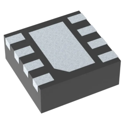
采用 2mm x 2mm 晶圆级小外形无引线 (WSON)-8
封装
TPS62160-Q1 是一款易于使用的同步降压 DC-DC 转
换器,针对高功率密度的应用进行了优化。 该器件的
开关频率典型值高达 2.25MHz,允许使用小型电感
器,通过利用 DCS-Control™ 拓扑技术提供快速的瞬
态响应并实现高输出电压精度。
此器件具有 3V 至 17V 宽运行输入电压范围,非常适
用于由锂离子或其它电池以及 12V 中间电源轨供电的
系统。 其输出电压为 0.9V 至 6V,支持高达 1A 的持
续输出电流(使用 100% 占空比模式)。
通过配置使能引脚和开漏电源正常状态引脚也可以实现
电源排序。
在节能模式下,器件可根据输入电压 (VIN) 生成约
17μA 的静态电流。 负载较小时可自动且无缝进入节能
模式,同时该模式可保持整个负载范围内的高效率。
在关断模式下,此器件会关闭且关断期间的流耗少于
2μA。
此器件采用 2mm × 2mm (DSG) 8 引脚 WSON 封装。
器件信息(1)
器件型号
2 应用
•
•
•
•
TPS62160-Q1
汽车类 12V 导轨式电源
以太网供电 (POE) 的同轴负载点 (POL) 电源
摄像机模块、视频模块
低压降稳压器 (LDO)
封装
WSON (8)
封装尺寸(标称值)
2.00mm x 2.00mm
(1) 要了解所有可用封装,请见数据表末尾的可订购产品附录。
4 简化电路原理图
VIN
3.3V / 1A
2.2µH
10uF
VIN
SW
EN
VOS
TPS62160-Q1
AGND
PG
PGND
FB
100k
470k
22uF
150k
1
PRODUCTION DATA information is current as of publication date. Products conform to specifications per the terms of the Texas
Instruments standard warranty. Production processing does not necessarily include testing of all parameters.
English Data Sheet: SLVSCK6
�TPS62160-Q1
ZHCSD49 – DECEMBER 2014
www.ti.com.cn
目录
1
2
3
4
5
6
7
8
特性 ..........................................................................
应用 ..........................................................................
说明 ..........................................................................
简化电路原理图 ........................................................
修订历史记录 ...........................................................
Pin Configuration and Functions .........................
Specifications.........................................................
1
1
1
1
2
3
4
7.1
7.2
7.3
7.4
7.5
7.6
4
4
4
4
5
6
Absolute Maximum Ratings ......................................
ESD Ratings..............................................................
Recommended Operating Conditions.......................
Thermal Information ..................................................
Electrical Characteristics...........................................
Typical Characteristics ..............................................
8.4 Device Functional Modes.......................................... 8
9
Application and Implementation ........................ 11
9.1 Application Information............................................ 11
9.2 Typical TPS62160-Q1 Application ......................... 11
9.3 System Examples ................................................... 19
10 Power Supply Recommendations ..................... 21
11 Layout................................................................... 22
11.1 Layout Guidelines ................................................. 22
11.2 Layout Example .................................................... 22
11.3 Thermal Considerations ........................................ 23
12 器件和文档支持 ..................................................... 24
12.1
12.2
12.3
12.4
12.5
Detailed Description .............................................. 7
8.1 Overview ................................................................... 7
8.2 Functional Block Diagram ......................................... 7
8.3 Feature Description................................................... 8
器件支持 ...............................................................
文档支持 ...............................................................
商标 .......................................................................
静电放电警告.........................................................
术语表 ...................................................................
24
24
24
24
24
13 机械封装和可订购信息 .......................................... 24
5 修订历史记录
2
日期
修订版本
注释
2014年12月
*
最初发布。
Copyright © 2014, Texas Instruments Incorporated
�TPS62160-Q1
www.ti.com.cn
ZHCSD49 – DECEMBER 2014
6 Pin Configuration and Functions
space
8-Pin WSON
DSG Package
(Top View)
PGND
1
VIN
2
EN
3
AGND
4
Exposed
Thermal
Pad
8
PG
7
SW
6
VOS
5
FB
space
space
Pin Functions
PIN (1)
NAME
NUMBER
I/O
DESCRIPTION
PGND
1
VIN
2
I
Supply voltage
EN
3
I
Enable input (High = enabled, Low = disabled)
AGND
4
FB
5
I
Voltage feedback of adjustable version. Connect resistive voltage divider to this pin. It is
recommended to connect FB to AGND on fixed output voltage versions for improved thermal
performance.
VOS
6
I
Output voltage sense pin and connection for the control loop circuitry.
SW
7
O
Switch node, which is connected to the internal MOSFET switches. Connect inductor between SW and
output capacitor.
PG
8
O
Exposed
Thermal Pad
(1)
Power ground
Analog Ground
Output power good (High = VOUT ready, Low = VOUT below nominal regulation) ; open drain
(requires pull-up resistor; goes high impedance, when device is switched off)
Must be connected to AGND. Must be soldered to achieve appropriate power dissipation and
mechanical reliability.
For more information about connecting pins, see Detailed Description and Application Information sections.
Copyright © 2014, Texas Instruments Incorporated
3
�TPS62160-Q1
ZHCSD49 – DECEMBER 2014
www.ti.com.cn
7 Specifications
7.1 Absolute Maximum Ratings
over operating junction temperature range (unless otherwise noted) (1)
Pin voltage range
(2)
Power Good sink current
MIN
MAX
VIN
–0.3
20
V
EN, SW
–0.3
VIN+0.3
V
FB, PG, VOS
–0.3
7
V
10
mA
PG
UNIT
Operating junction temperature range, TJ
–40
125
°C
Storage temperature range, Tstg
–65
150
°C
(1)
(2)
Stresses beyond those listed under absolute maximum ratings may cause permanent damage to the device. These are stress ratings
only, and functional operation of the device at these or any other conditions beyond those indicated under recommended operating
conditions is not implied. Exposure to absolute-maximum-rated conditions for extended periods my affect device reliability.
All voltages are with respect to network ground terminal.
7.2 ESD Ratings
VALUE
V(ESD)
(1)
Electrostatic discharge
Human body model (HBM), per AEC Q100-002 (1)
±2000
Charged device model (CDM), per AEC Q100-011
±500
UNIT
V
AEC Q100-002 indicates HBM stressing is done in accordance with the ANSI/ESDA/JEDEC JS-001 specification.
7.3 Recommended Operating Conditions
over operating junction temperature range (unless otherwise noted)
MIN
TYP
MAX
UNIT
VIN
Supply voltage
3
17
VOUT
Output voltage range
0.9
6
V
V
TJ
Operating junction temperature
–40
125
°C
7.4 Thermal Information
THERMAL METRIC (1)
TPS62160-Q1
DSG (8 PINS)
DGK (8 PINS)
184.3
RθJA
Junction-to-ambient thermal resistance
61.8
RθJC(top)
Junction-to-case (top) thermal resistance
61.3
74.6
RθJB
Junction-to-board thermal resistance
15.5
105.8
ψJT
Junction-to-top characterization parameter
0.4
13.3
ψJB
Junction-to-board characterization parameter
15.4
104.2
RθJC(bot)
Junction-to-case (bottom) thermal resistance
8.6
-
(1)
4
UNIT
°C/W
For more information about traditional and new thermal metrics, see the IC Package Thermal Metrics application report, SPRA953.
Copyright © 2014, Texas Instruments Incorporated
�TPS62160-Q1
www.ti.com.cn
ZHCSD49 – DECEMBER 2014
7.5 Electrical Characteristics
Over junction temperature range (TJ = –40°C to +125°C), typical values at VIN = 12 V and TJ = 25°C (unless otherwise noted)
PARAMETER
TEST CONDITIONS
MIN
TYP
MAX
UNIT
SUPPLY
VIN
Input voltage range (1)
17
V
IQ
Operating quiescent current
EN = High, IOUT = 0 mA, Device not switching
17
30
µA
ISD
Shutdown current (2)
EN = Low
1.8
25
µA
VUVLO
Undervoltage lockout threshold
2.7
2.82
3
Falling input voltage
2.6
Hysteresis
180
Thermal shutdown temperature
TSD
160
Thermal shutdown hysteresis
V
mV
°C
20
CONTROL (EN, PG)
VEN_H
High level input threshold voltage (EN)
0.9
VEN_L
Low level input threshold voltage (EN)
ILKG_EN
Input leakage current (EN)
VTH_PG
Power Good threshold voltage
VOL_PG
Power Good output low
IPG = –2 mA
0.07
0.3
V
ILKG_PG
Input leakage current (PG)
VPG = 1.8 V
1
400
nA
VIN ≥ 6 V
300
600
VIN = 3 V
430
VIN ≥ 6 V
120
VIN = 3 V
165
EN = VIN or GND
V
0.3
V
0.01
1
µA
Rising (%VOUT)
92%
95%
98%
Falling (%VOUT)
87%
90%
93%
POWER SWITCH
High-side MOSFET ON-resistance
RDS(ON)
Low-side MOSFET ON-resistance
ILIMF
High-side MOSFET forward current
limit (3)
VIN = 12 V, TA = 25°C
1.45
1.95
200
mΩ
mΩ
2.45
A
400
nA
0.9
6.0
V
PWM Mode operation, VIN ≥ VOUT + 1 V
–3%
3%
Power Save Mode operation, COUT = 2x22 µF (4)
–3%
OUTPUT
VREF
Internal reference voltage
ILKG_FB
Pin leakage current (FB)
VFB = 1.2 V
0.8
Output voltage range
VIN ≥ VOUT
Feedback voltage accuracy
VOUT
DC output voltage load regulation (5)
DC output voltage line regulation
(1)
(2)
(3)
(4)
(5)
(5)
5
V
4%
VIN = 12 V, VOUT = 3.3 V, PWM Mode operation
0.05
%/A
3 V ≤ VIN ≤ 17 V, VOUT = 3.3 V, IOUT = 0.5 A,
PWM Mode operation
0.02
%/V
The device is still functional down to Under Voltage Lockout (see parameter VUVLO).
Current into VIN pin.
This is the static current limit. It can be temporarily higher in applications due to internal propagation delay (see Current Limit and Short
Circuit Protection section).
The accuracy in Power Save Mode can be improved by increasing the COUT value, reducing the output voltage ripple.
Line and load regulation are depending on external component selection and layout (see Figure 14 and Figure 15).
Copyright © 2014, Texas Instruments Incorporated
5
�TPS62160-Q1
ZHCSD49 – DECEMBER 2014
www.ti.com.cn
7.6 Typical Characteristics
At VIN = 12 V, VOUT = 3.3 V and TJ = 25°C (unless otherwise noted)
6
Figure 1. Quiescent Current
Figure 2. Shutdown Current
Figure 3. High-Side Static Drain-Source-Resistance (RDSon)
Figure 4. Low-Side Static Drain-Source-Resistance (RDSon)
Copyright © 2014, Texas Instruments Incorporated
�TPS62160-Q1
www.ti.com.cn
ZHCSD49 – DECEMBER 2014
8 Detailed Description
8.1 Overview
The TPS62160-Q1 synchronous switched mode power converter is based on DCS-Control™ (Direct Control with
Seamless transition into power
save mode), an advanced regulation topology, that combines the advantages of hysteretic, voltage mode and
current mode control including an AC loop directly associated to the output voltage. This control loop takes
information about output voltage changes and feeds it directly to a fast comparator stage. It sets the switching
frequency, which is constant for steady state operating conditions, and provides immediate response to dynamic
load changes. To get accurate DC load regulation, a voltage feedback loop is used. The internally compensated
regulation network achieves fast and stable operation with small external components and low ESR capacitors.
The DCS-Control™ topology supports PWM (Pulse Width Modulation) mode for medium and heavy load
conditions and a Power Save Mode at light loads. During PWM, it operates at its nominal switching frequency in
continuous conduction mode. This frequency is typically about 2.25 MHz with a controlled frequency variation
depending on the input voltage. If the load current decreases, the converter enters Power Save Mode to sustain
high efficiency down to very light loads. In Power Save Mode the switching frequency decreases linearly with the
load current. Since DCS-Control™ supports both operation modes within one single building block, the transition
from PWM to Power Save Mode is seamless without effects on the output voltage.
8.2 Functional Block Diagram
PG
Soft
start
Thermal
Shtdwn
UVLO
VIN
PG control
HS lim
comp
power
control
control logic
EN*
gate
drive
SW
comp
LS lim
VOS
direct control
&
compensation
ramp
_
FB
comparator
+
timer tON
error
amplifier
DCS - ControlTM
*
This pin is connected to a pull down resistor internally
(see Detailed Description section).
Copyright © 2014, Texas Instruments Incorporated
AGND
PGND
7
�TPS62160-Q1
ZHCSD49 – DECEMBER 2014
www.ti.com.cn
8.3 Feature Description
8.3.1 Enable / Shutdown (EN)
When Enable (EN) is set High, the device starts operation.
Shutdown is forced if EN is pulled Low with a shutdown current of typically 1.5 µA. During shutdown, the internal
power MOSFETs as well as the entire control circuitry are turned off. The internal resistive divider pulls down the
output voltage smoothly. If the EN pin is Low, an internal pull-down resistor of about 400 kΩ is connected and
keeps it Low in case of floating pin.
Connecting the EN pin to an appropriate output signal of another power rail provides sequencing of multiple
power rails.
8.3.2 Softstart
The internal soft start circuitry controls the output voltage slope during startup. This avoids excessive inrush
current and ensures a controlled output voltage rise time. It also prevents unwanted voltage drops from highimpedance power sources or batteries. When EN is set to start device operation, the device starts switching after
a delay of about 50 µs and VOUT rises with a slope of about 25 mV/µs. See Figure 26 and Figure 27 for typical
startup operation.
The TPS62160-Q1 can start into a pre-biased output. During monotonic pre-biased startup, the low-side
MOSFET is not allowed to turn on until the device's internal ramp sets an output voltage above the pre-bias
voltage.
8.3.3 Power Good (PG)
The TPS62160-Q1 has a built in power good (PG) function to indicate whether the output voltage has reached its
appropriate level or not. The PG signal can be used for startup sequencing of multiple rails. The PG pin is an
open-drain output that requires a pull-up resistor (to any voltage below 7 V). It can sink 2 mA of current and
maintain its specified logic low level. It is high impedance when the device is turned off due to EN, UVLO or
thermal shutdown.
8.3.4 Under Voltage Lockout (UVLO)
If the input voltage drops, the under voltage lockout prevents misoperation of the device by switching off both the
power FETs. The under voltage lockout threshold is set typically to 2.7 V. The device is fully operational for
voltages above the UVLO threshold and turns off if the input voltage trips the threshold. The converter starts
operation again once the input voltage exceeds the threshold by a hysteresis of typically 180 mV.
8.3.5 Thermal Shutdown
The junction temperature (TJ) of the device is monitored by an internal temperature sensor. If TJ exceeds 160°C
(typ), the device goes into thermal shut down. Both the high-side and low-side power FETs are turned off and PG
goes high impedance. When TJ decreases below the hysteresis amount, the converter resumes normal
operation, beginning with Soft Start. To avoid unstable conditions, a hysteresis of typically 20°C is implemented
on the thermal shut down temperature.
8.4 Device Functional Modes
8.4.1 Pulse Width Modulation (PWM) Operation
The TPS62160-Q1 operates with pulse width modulation in continuous conduction mode (CCM) with a nominal
switching frequency of about 2.25 MHz. The frequency variation in PWM is controlled and depends on VIN, VOUT
and the inductance. The device operates in PWM mode as long the output current is higher than half the
inductor's ripple current. To maintain high efficiency at light loads, the device enters Power Save Mode at the
boundary to discontinuous conduction mode (DCM). This happens if the output current becomes smaller than
half the inductor's ripple current.
8
Copyright © 2014, Texas Instruments Incorporated
�TPS62160-Q1
www.ti.com.cn
ZHCSD49 – DECEMBER 2014
Device Functional Modes (continued)
8.4.2 Power Save Operation
The TPS62160-Q1's built in Power Save Mode will be entered seamlessly, if the load current decreases. This
secures a high efficiency in light load operation. The device remains in Power Save Mode as long as the inductor
current is discontinuous.
In Power Save Mode the switching frequency decreases linearly with the load current maintaining high efficiency.
The transition into and out of Power Save Mode happens within the entire regulation scheme and is seamless in
both directions.
The TPS62160-Q1 includes a fixed on-time circuitry. This on-time, in steady-state operation, can be estimated
as:
space
t ON =
VOUT
´ 420ns
VIN
(1)
space
For very small output voltages, the on-time increases beyond the result of Equation 1, to stay above an absolute
minimum on-time, tON(min), which is around 80 ns to limit switching losses. The peak inductor current in PSM can
be approximated by:
space
ILPSM(peak) =
(VIN - VOUT )
L
´ t ON
(2)
space
When VIN decreases to typically 15% above VOUT, the TPS62160-Q1 does not enter Power Save Mode,
regardless of the load current. The device maintains output regulation in PWM mode.
8.4.3 100% Duty-Cycle Operation
The duty cycle of the buck converter is given by D = Vout/Vin and increases as the input voltage comes close to
the output voltage. In this case, the device starts 100% duty cycle operation turning on the high-side switch
100% of the time. The high-side switch stays turned on as long as the output voltage is below the internal set
point. This allows the conversion of small input to output voltage differences, e.g. for longest operation time of
battery-powered applications. In 100% duty cycle mode, the low-side FET is switched off.
The minimum input voltage to maintain output voltage regulation, depending on the load current and the output
voltage level, can be calculated as:
space
(
VIN(min) = VOUT(min) + IOUT RDS(on) + RL
)
(3)
where
IOUT is the output current,
RDS(on) is the RDS(on) of the high-side FET and
RL is the DC resistance of the inductor used.
space
8.4.4 Current Limit and Short Circuit Protection
The TPS62160-Q1 is protected against heavy load and short circuit events. At heavy loads, the current limit
determines the maximum output current. If the current limit is reached, the high-side FET will be turned off.
Avoiding shoot through current, the low-side FET will be switched on to sink the inductor current. The high-side
FET will turn on again, only if the current in the low-side FET has decreased below the low side current limit
threshold.
Copyright © 2014, Texas Instruments Incorporated
9
�TPS62160-Q1
ZHCSD49 – DECEMBER 2014
www.ti.com.cn
Device Functional Modes (continued)
The output current of the device is limited by the current limit (see Electrical Characteristics). Due to internal
propagation delay, the actual current can exceed the static current limit during that time. The dynamic current
limit can be calculated as follows:
space
Ipeak(typ) = ILIMF +
VL
´ tPD
L
(4)
where
ILIMF is the static current limit, specified in the electrical characteristic table,
L is the inductor value,
VL is the voltage across the inductor and
tPD is the internal propagation delay.
space
The dynamic high side switch peak current can be calculated as follows:
space
Ipeak(typ) = ILIMF _ HS +
(VIN - VOUT )
L
´ 30ns
(5)
space
Care on the current limit has to be taken if the input voltage is high and very small inductances are used.
8.4.5 Operation Above TJ = 125°C
The operating junction temperature of the device is specified up to 125°C. In power supply circuits, the self
heating effect causes, that the junction temperature, TJ, is even higher than the ambient temperature TA.
Depending on TA and the load current, the maximum operating temperature TJ can be exceeded. However, the
electrical characteristics are specified up to a TJ of 125°C only. The device operates as long as thermal
shutdown threshold is not triggered.
10
Copyright © 2014, Texas Instruments Incorporated
�TPS62160-Q1
www.ti.com.cn
ZHCSD49 – DECEMBER 2014
9 Application and Implementation
9.1 Application Information
The TPS62160-Q1 is a synchronous switched mode step-down converter, able to convert a 3 V to 17 V input
voltage into a lower, 0.9 V to 6 V, output voltage, providing up to 1-A load current. The following section gives
guidance on the external component selection to operate the device within the recommended operating
conditions.
9.2 Typical TPS62160-Q1 Application
space
space
VIN
3.3V / 1A
2.2µH
10uF
VIN
SW
EN
VOS
TPS62160-Q1
AGND
PG
PGND
FB
100k
470k
22uF
150k
Figure 5. 3.3-V / 1-A Power Supply
space
9.2.1 Design Requirements
The step-down converter design can be adapted to different output voltage and load current needs by choosing
external components appropriate. The following design procedure is adequate for whole VIN, VOUT, and load
current range of TPS62160-Q1. Using Table 2, the design procedure needs minimum effort.
space
Table 1. Components Used for Application Characteristics
REFERENCE
DESCRIPTION
IC
17-V, 1-A step-down converter, WSON
L1
2.2-µH, 1.4-A, 3 x 2.8 x 1.2 mm
MANUFACTURER
TPS62160QDSG, Texas Instruments
VLF3012ST-2R2M1R4, TDK
CIN
10-µF, 25-V, ceramic
Standard
COUT
22-µF, 6.3-V, ceramic
Standard
R1
Depending on Vout
R2
Depending on Vout
R3
100-kΩ, chip, 0603, 1/16-W, 1%
Standard
space
9.2.2 Detailed Design Procedure
9.2.2.1 Programming the Output Voltage
The TPS62160-Q1 can be programmed for output voltages from 0.9 V to 6 V by using a resistive divider from
VOUT to FB to AGND. The voltage at the FB pin is regulated to 800 mV. The value of the output voltage is set
by the selection of the resistive divider from Equation 6. It is recommended to choose resistor values which allow
a cross current of at least 2 uA, meaning the value of R2 should not exceed 400 kΩ. Lower resistor values are
recommended for highest accuracy and most robust design. For applications requiring lowest current
consumption, the use of fixed output voltage versions is recommended.
space
Copyright © 2014, Texas Instruments Incorporated
11
�TPS62160-Q1
ZHCSD49 – DECEMBER 2014
www.ti.com.cn
æV
ö
R1 = R2 ç OUT - 1÷
è VREF
ø
(6)
space
In case the FB pin gets opened, the device clamps the output voltage at the VOS pin to about 7.4 V.
9.2.2.2 External Component Selection
The external components have to fulfill the needs of the application, but also the stability criteria of the devices
control loop. The TPS62160-Q1 is optimized to work within a range of external components. The LC output filters
inductance and capacitance have to be considered together, creating a double pole, responsible for the corner
frequency of the converter (see Output Filter And Loop Stability section). Table 2 can be used to simplify the
output filter component selection.
space
Table 2. Recommended LC Output Filter Combinations (1)
4.7µF
10µF
22µF
47µF
100µF
200µF
2.2µH
√
√ (2)
√
√
√
3.3µH
√
√
√
√
400µF
1µH
4.7µH
(1)
(2)
The values in the table are nominal values. Variations of typically ±20% due to tolerance, saturation and DC bias are assumed.
This LC combination is the standard value and recommended for most applications.
More detailed information on further LC combinations can be found in SLVA463.
9.2.2.2.1 Inductor Selection
The inductor selection is affected by several effects like inductor ripple current, output ripple voltage, PWM-toPSM transition point and efficiency. In addition, the inductor selected has to be rated for appropriate saturation
current and DC resistance (DCR). Equation 7 and Equation 8 calculate the maximum inductor current under
static load conditions.
spacer
IL(max) = IOUT(max) +
DIL(max)
2
(7)
spacer
DIL(max)
VOUT
æ
ç 1- V
IN(max)
= VOUT ´ ç
ç L(min) ´ ƒSW
çç
è
ö
÷
÷
÷
÷÷
ø
(8)
where
IL(max) is the maximum inductor current,
ΔIL is the Peak-to-Peak Inductor Ripple Current,
L(min) is the minimum effective inductor value and
fSW is the actual PWM Switching Frequency.
spacer
Calculating the maximum inductor current using the actual operating conditions gives the minimum saturation
current of the inductor needed. A margin of about 20% is recommended to add. A larger inductor value is also
useful to get lower ripple current, but increases the transient response time and size as well. The following
inductors have been used with the TPS62160-Q1 and are recommended for use:
12
Copyright © 2014, Texas Instruments Incorporated
�TPS62160-Q1
www.ti.com.cn
ZHCSD49 – DECEMBER 2014
Table 3. List of Inductors
(1)
TYPE
INDUCTANCE [µH]
CURRENT [A] (1)
DIMENSIONS [L x B x H] mm
MANUFACTURER
VLF3012ST-2R2M1R4
2.2 µH, ±20%
1.9 A
3.0 x 2.8 x 1.2
TDK
TDK
VLF302512MT-2R2M
2.2 µH, ±20%
1.9 A
3.0 x 2.5 x 1.2
VLS252012T-2R2M1R3
2.2 µH, ±20%
1.3 A
2.5 x 2.0 x 1.2
TDK
XFL3012-222MEC
2.2 µH, ±20%
1.9 A
3.0 x 3.0 x 1.2
Coilcraft
XFL3012-332MEC
3.3 µH, ±20%
1.6 A
3.0 x 3.0 x 1.2
Coilcraft
LPS3015-332ML_
3.3 µH, ±20%
1.4 A
3.0 x 3.0 x 1.4
Coilcraft
NR3015T-2R2M
2.2 µH, ±20%
1.5 A
3.0 x 3.0 x 1.5
Taiyo Yuden
744025003
3.3 µH, ±20%
1.5 A
2.8 x 2.8 x 2.8
Wuerth
PSI25201B-2R2MS
2.2 µH, ±20%
1.3 A
2.0 x 2.5 x 1.2
Cyntec
IRMS at 40°C rise or ISAT at 30% drop.
spacer
The TPS62160-Q1 can be run with an inductor as low as 2.2 µH. However, for applications with low input
voltages, 3.3 µH is recommended, to allow the full output current. The inductor value also determines the load
current at which Power Save Mode is entered:
space
Iload(PSM) =
1
DIL
2
(9)
space
Using Equation 8, this current level can be adjusted by changing the inductor value.
9.2.2.2.2 Capacitor Selection
9.2.2.2.2.1 Output Capacitor
The recommended value for the output capacitor is 22 uF. The architecture of the TPS62160-Q1 allows the use
of tiny ceramic output capacitors with low equivalent series resistance (ESR). These capacitors provide low
output voltage ripple and are recommended. To keep its low resistance up to high frequencies and to get narrow
capacitance variation with temperature, it's recommended to use X7R or X5R dielectric. Using a higher value can
have some advantages like smaller voltage ripple and a tighter DC output accuracy in Power Save Mode (see
SLVA463).
NOTE
In power save mode, the output voltage ripple depends on the output capacitance, its ESR
and the peak inductor current. Using ceramic capacitors provides small ESR and low
ripple.
9.2.2.2.2.2 Input Capacitor
For most applications, 10 µF is sufficient and is recommended, though a larger value reduces input current ripple
further. The input capacitor buffers the input voltage for transient events and also decouples the converter from
the supply. A low ESR multilayer ceramic capacitor is recommended for best filtering and should be placed
between VIN and GND as close as possible to those pins.
spacer
NOTE
DC Bias effect: High capacitance ceramic capacitors have a DC Bias effect, which will
have a strong influence on the final effective capacitance. Therefore the right capacitor
value has to be chosen carefully. Package size and voltage rating in combination with
dielectric material are responsible for differences between the rated capacitor value and
the effective capacitance.
Copyright © 2014, Texas Instruments Incorporated
13
�TPS62160-Q1
ZHCSD49 – DECEMBER 2014
www.ti.com.cn
9.2.2.3 Output Filter And Loop Stability
The TPS62160-Q1 is internally compensated to be stable with L-C filter combinations corresponding to a corner
frequency to be calculated with Equation 10:
space
ƒLC =
1
2p L ´ C
(10)
space
Proven nominal values for inductance and ceramic capacitance are given in Table 2 and are recommended for
use. Different values may work, but care has to be taken on the loop stability which might be affected. More
information including a detailed L-C stability matrix can be found in SLVA463.
The TPS62160-Q1 includes an internal 25-pF feedforward capacitor, connected between the VOS and FB pins.
This capacitor impacts the frequency behavior and sets a pole and zero in the control loop with the resistors of
the feedback divider, per Equation 11 and Equation 12:
space
ƒ zero =
1
2p ´ R1 ´ 25 pF
(11)
æ 1
1
1 ö
´ç
+
÷
2p ´ 25 pF è R1 R2 ø
(12)
space
ƒpole =
space
Though the TPS62160-Q1 is stable without the pole and zero being in a particular location, adjusting their
location to the specific needs of the application can provide better performance in Power Save mode and/or
improved transient response. An external feedforward capacitor can also be added. A more detailed discussion
on the optimization for stability vs transient response can be found in SLVA289 and SLVA466.
If using ceramic capacitors, the DC bias effect has to be considered. The DC bias effect results in a drop in
effective capacitance as the voltage across the capacitor increases (see NOTE in DC Bias effect section).
9.2.3 Application Performance Plots
At VIN = 12 V, VOUT = 3.3 V and TJ = 25°C (unless otherwise noted)
100.0
100.0
90.0
90.0
80.0
70.0
VIN=17V
60.0
50.0
VIN=12V
40.0
30.0
70.0
IOUT=1A
50.0
40.0
20.0
10.0
10.0
0.01
Output Current (A)
IOUT=100mA
IOUT=10mA
30.0
VIN=6V
0.001
IOUT=1mA
60.0
20.0
0.0
0.0001
0.1
Vout = 6 V
Figure 6. Efficiency vs Output Current
14
Efficiency (%)
Efficiency (%)
80.0
1
0.0
7
8
9
G001
10
11
12
13
14
Input Voltage (V)
15
16
17
G001
Vout = 6 V
Figure 7. Efficiency vs Input Voltage
Copyright © 2014, Texas Instruments Incorporated
�TPS62160-Q1
www.ti.com.cn
ZHCSD49 – DECEMBER 2014
100.0
100.0
90.0
90.0
80.0
80.0
70.0
70.0
60.0
Efficiency (%)
Efficiency (%)
At VIN = 12 V, VOUT = 3.3 V and TJ = 25°C (unless otherwise noted)
VIN=17V
50.0
VIN=12V
40.0
VIN=5V
20.0
10.0
10.0
0.1
0.0
1
4
5
80.0
70.0
70.0
60.0
VIN=17V
50.0
40.0
VIN=12V
60.0
20.0
20.0
10.0
10.0
0.1
0.0
1
IOUT=100mA
3
4
5
6
7
G001
Vout = 1.8 V
IOUT=10mA
40.0
30.0
0.01
Output Current (A)
IOUT=1mA
50.0
30.0
0.001
IOUT=500mA
90.0
80.0
Efficiency (%)
Efficiency (%)
9 10 11 12 13 14 15 16 17
Input Voltage (V)
G001
100.0
VIN=5V
0.0
0.0001
8 9 10 11 12 13 14 15 16 17
Input Voltage (V)
G001
Vout = 1.8 V
Figure 10. Efficiency vs Output Current
Figure 11. Efficiency vs Input Voltage
100.0
100.0
90.0
90.0
VIN=5V
70.0
60.0
50.0
VIN=17V
40.0
VIN=12V
30.0
50.0
30.0
10.0
0.1
Vout = 0.9 V
Figure 12. Efficiency vs Output Current
Copyright © 2014, Texas Instruments Incorporated
IOUT=1mA
40.0
20.0
0.01
Output Current (A)
IOUT=1A
60.0
10.0
0.001
IOUT=100mA
70.0
20.0
0.0
0.0001
IOUT=10mA
80.0
Efficiency (%)
Efficiency (%)
8
Figure 9. Efficiency vs Input Voltage
100.0
80.0
7
Vout = 3.3 V
Figure 8. Efficiency vs Output Current
90.0
6
G001
Vout = 3.3 V
IOUT=100mA
40.0
30.0
0.01
Output Current (A)
IOUT=10mA
50.0
20.0
0.001
IOUT=1mA
60.0
30.0
0.0
0.0001
IOUT=1A
1
0.0
3
4
5
G001
6
7
8 9 10 11 12 13 14 15 16 17
Input Voltage (V)
G001
Vout = 0.9 V
Figure 13. Efficiency vs Input Voltage
15
�TPS62160-Q1
ZHCSD49 – DECEMBER 2014
www.ti.com.cn
At VIN = 12 V, VOUT = 3.3 V and TJ = 25°C (unless otherwise noted)
3.35
Output Voltage (V)
Output Voltage (V)
3.35
3.30
VIN=5V
VIN=12V
VIN=17V
3.25
3.20
0.0001
0.001
0.01
Output Current (A)
0.1
4
4
3.5
3.5
Switching Frequency (MHz)
Switching Frequency (MHz)
IOUT=1A
4
7
10
13
Input Voltage (V)
3
2.5
2
1.5
1
16
G001
Figure 15. Output Voltage Accuracy (Line Regulation)
0.5
3
IOUT=1A
2.5
2
IOUT=0.5A
1.5
1
0.5
0
0.1
0.2
0.3
0.4 0.5 0.6 0.7
Output Current (A)
0.8
0.9
0
1
4
6
8
10
12
Input Voltage (V)
G000
Figure 16. Switching Frequency vs Output Current
14
16
18
G000
Figure 17. Switching Frequency vs Input Voltage
0.05
3
2.5
0.04
VIN=17V
Output Current (A)
Output Voltage Ripple (V)
IOUT=100mA
3.25
G001
Figure 14. Output Voltage Accuracy (Load Regulation)
0
IOUT=10mA
3.30
3.20
1
IOUT=1mA
0.03
0.02
VIN=12V
0.01
−40°C
2
25°C
1.5
1
85°C
0.5
VIN=5V
0
0
0.1
0.2
0.3
0.4 0.5 0.6 0.7
Output Current (A)
0.8
Figure 18. Output Voltage Ripple
16
0.9
1
G000
0
4
5
6
7
8
9 10 11 12 13 14 15 16 17
Input Voltage (V)
G000
Figure 19. Maximum Output Current
Copyright © 2014, Texas Instruments Incorporated
�TPS62160-Q1
www.ti.com.cn
ZHCSD49 – DECEMBER 2014
At VIN = 12 V, VOUT = 3.3 V and TJ = 25°C (unless otherwise noted)
Figure 20. PWM / PSM Mode Transitions
500 mA to 1 A
Figure 22. Load Transient Response in PWM Mode
Figure 21. PWM to PSM Mode Transition
100 mA to 500 mA
Figure 23. Load Transient Response from Power Save
Mode
500 mA to 1 A, Rising edge
500 mA to 1 A, Falling edge
Figure 24. Load Transient Response in PWM Mode
Figure 25. Load Transient Response in PWM Mode
Copyright © 2014, Texas Instruments Incorporated
17
�TPS62160-Q1
ZHCSD49 – DECEMBER 2014
www.ti.com.cn
At VIN = 12 V, VOUT = 3.3 V and TJ = 25°C (unless otherwise noted)
Iout = 100 mA
Iout = 1 A
Figure 26. Startup
Iout = 66 mA
Figure 28. Typical Operation in Power Save Mode
18
Figure 27. Startup
Iout = 1 A
Figure 29. Typical Operation in PWM Mode
Copyright © 2014, Texas Instruments Incorporated
�TPS62160-Q1
www.ti.com.cn
ZHCSD49 – DECEMBER 2014
9.3 System Examples
9.3.1 Inverting Power Supply
The TPS62160-Q1 can be used as inverting power supply by rearranging external circuitry as shown in
Figure 30. As the former GND node now represents a voltage level below system ground, the voltage difference
between VIN and VOUT has to be limited for operation to the maximum supply voltage of 17 V (see Equation 13).
spacer
VIN + VOUT £ VIN
(13)
max
space
10uF
2.2µH
(3 .. 12)V
VIN
SW
EN
10uF
VOS
PG
PGND
FB
680k
100k
TPS62160-Q1
GND
22uF
130k
-5V
Figure 30. –5-V Inverting Power Supply
space
The transfer function of the inverting power supply configuration differs from the buck mode transfer function,
incorporating a Right Half Plane Zero additionally. The loop stability has to be adapted and an output
capacitance of at least 22 µF is recommended. A detailed design example is given in SLVA469.
9.3.2 Various Output Voltages
The TPS62160-Q1 can be set for different output voltages between 0.9 V and 6 V. Some examples are shown
below.
space
space
(5 .. 17)V
10uF
5V / 1A
2.2µH
VIN
SW
EN
VOS
TPS62160-Q1
AGND
PG
PGND
FB
100k
680k
22uF
130k
Figure 31. 5-V/1-A Power Supply
space
space
Copyright © 2014, Texas Instruments Incorporated
19
�TPS62160-Q1
ZHCSD49 – DECEMBER 2014
www.ti.com.cn
System Examples (continued)
(3.3 .. 17)V
10uF
3.3V / 1A
2.2µH
VIN
SW
EN
VOS
TPS62160-Q1
AGND
PG
PGND
FB
100k
470k
22uF
150k
Figure 32. 3.3-V/1-A Power Supply
space
space
(3 .. 17)V
10uF
2.5V / 1A
2.2µH
VIN
SW
EN
VOS
TPS62160-Q1
AGND
PG
PGND
FB
100k
390k
22uF
180k
Figure 33. 2.5-V/1-A Power Supply
space
space
(3 .. 17)V
10uF
1.8V / 1A
2.2µH
VIN
SW
EN
VOS
TPS62160-Q1
AGND
PG
PGND
FB
100k
200k
22uF
160k
Figure 34. 1.8-V/1-A Power Supply
space
space
(3 .. 17)V
10uF
1.5V / 1A
2.2µH
VIN
SW
EN
VOS
TPS62160-Q1
AGND
PG
PGND
FB
100k
130k
22uF
150k
Figure 35. 1.5-V/1-A Power Supply
space
space
20
Copyright © 2014, Texas Instruments Incorporated
�TPS62160-Q1
www.ti.com.cn
ZHCSD49 – DECEMBER 2014
System Examples (continued)
(3 .. 17)V
10uF
1.2V / 1A
2.2µH
VIN
SW
EN
VOS
TPS62160-Q1
AGND
PG
PGND
FB
100k
75k
22uF
150k
Figure 36. 1.2-V/1-A Power Supply
space
space
(3 .. 17)V
10uF
1V / 1A
2.2µH
VIN
SW
EN
VOS
TPS62160-Q1
AGND
PG
PGND
FB
100k
51k
22uF
200k
Figure 37. 1-V/1-A Power Supply
space
10 Power Supply Recommendations
The TPS62160-Q1 is designed to operate from a 3-V to 17-V input voltage supply. The input power supply's
output current needs to be rated according to the output voltage and the output current of the power rail
application.
Copyright © 2014, Texas Instruments Incorporated
21
�TPS62160-Q1
ZHCSD49 – DECEMBER 2014
www.ti.com.cn
11 Layout
11.1 Layout Guidelines
A proper layout is critical for the operation of a switched mode power supply, even more at high switching
frequencies. Therefore the PCB layout of the TPS62160-Q1 demands careful attention to ensure operation and
to get the performance specified. A poor layout can lead to issues like poor regulation (both line and load),
stability and accuracy weaknesses, increased EMI radiation and noise sensitivity. Considering the following
topics ensures best electrical and optimized thermal performance:
1) The input capacitor must be placed as close as possible to the VIN and PGND pin of the IC. This provides low
resistive and inductive path for the high di/dt input current.
2) The VOS pin must be connect in the shortest way to VOUT at the output capacitor - avoiding noise coupling.
3) The feedback resistors, R1 and R2 must be connected close to the FB and AGND pins - avoiding noise
coupling.
4) The output capacitor should be placed such that its ground is as close as possible to the IC's PGND pins avoiding additional voltage drop in traces.
5) The inductor should be placed close to the SW pin and connect directly to the output capacitor - minimizing
the loop area between the SW pin, inductor, output capacitor and PGND pin.
More detailed information can be found in the EVM Users Guide, SLVU483.
The Exposed Thermal Pad must be soldered to the circuit board for mechanical reliability and to achieve
appropriate power dissipation. Although the Exposed Thermal Pad can be connected to a floating circuit board
trace, the device will have better thermal performance if it is connected to a larger ground plane. The Exposed
Thermal Pad is electrically connected to AGND.
PGND
COUT
VOUT
11.2 Layout Example
CIN
L
VIN
AGND
R2
R1
VIN
Figure 38. Layout Example
22
Copyright © 2014, Texas Instruments Incorporated
�TPS62160-Q1
www.ti.com.cn
ZHCSD49 – DECEMBER 2014
11.3 Thermal Considerations
Implementation of integrated circuits in low-profile and fine-pitch surface-mount packages typically requires
special attention to power dissipation. Many system-dependent issues such as thermal coupling, airflow, added
heat sinks and convection surfaces, and the presence of other heat-generating components affect the powerdissipation limits of a given component.
Three basic approaches for enhancing thermal performance are listed below:
• Improving the power dissipation capability of the PCB design
• Improving the thermal coupling of the component to the PCB by soldering the Exposed Thermal Pad
• Introducing airflow in the system
For more details on how to use the thermal parameters, see the application notes: Thermal Characteristics
Application Note (SZZA017), and (SPRA953).
The TPS62160-Q1 is designed for a maximum operating junction temperature (TJ) of 125°C. Therefore the
maximum output power is limited by the power losses that can be dissipated over the actual thermal resistance,
given by the package and the surrounding PCB structures. Since the thermal resistance of the package is fixed,
increasing the size of the surrounding copper area and improving the thermal connection to the IC can reduce
the thermal resistance. To get an improved thermal behavior, it's recommended to use top layer metal to connect
the device with wide and thick metal lines. Internal ground layers can connect to vias directly under the IC for
improved thermal performance.
If short circuit or overload conditions are present, the device is protected by limiting internal power dissipation.
版权 © 2014, Texas Instruments Incorporated
23
�TPS62160-Q1
ZHCSD49 – DECEMBER 2014
www.ti.com.cn
12 器件和文档支持
12.1 器件支持
12.1.1 第三方产品免责声明
TI 发布的与第三方产品或服务有关的信息,不能构成与此类产品或服务或保修的适用性有关的认可,不能构成此类
产品或服务单独或与任何 TI 产品或服务一起的表示或认可。
12.2 文档支持
12.2.1 相关文档
应用报告《优化 TPS62130/40/50/60/70 输出滤波器》(文献编号:SLVA463)
应用报告《采用前馈电容优化内部补偿 DC-DC 转换器的瞬态响应》(文献编号:SLVA289)
应用报告《采用前馈电容优化 TPS62130/40/50/60/70 的稳定性和带宽》(文件编号:SLVA466)
用户指南《TPS62160EVM-627 和 TPS62170EVM-627 评估模块》(文献编号:SLVU483)
应用报告《采用 JEDEC PCB 设计的线性和逻辑封装散热特性》(文件编号:SZZA017)
应用报告《半导体和 IC 封装热指标》(文件编号:SPRA953)
12.3 商标
DCS-Control is a trademark of Texas Instruments.
12.4 静电放电警告
这些装置包含有限的内置 ESD 保护。 存储或装卸时,应将导线一起截短或将装置放置于导电泡棉中,以防止 MOS 门极遭受静电损
伤。
12.5 术语表
SLYZ022 — TI 术语表。
这份术语表列出并解释术语、首字母缩略词和定义。
13 机械封装和可订购信息
以下页中包括机械封装和可订购信息。 这些信息是针对指定器件可提供的最新数据。 这些数据会在无通知且不对
本文档进行修订的情况下发生改变。 欲获得该数据表的浏览器版本,请查阅左侧的导航栏。
24
版权 © 2014, Texas Instruments Incorporated
�PACKAGE OPTION ADDENDUM
www.ti.com
10-Dec-2020
PACKAGING INFORMATION
Orderable Device
Status
(1)
Package Type Package Pins Package
Drawing
Qty
Eco Plan
(2)
Lead finish/
Ball material
MSL Peak Temp
Op Temp (°C)
Device Marking
(3)
(4/5)
(6)
TPS62160QDSGRQ1
ACTIVE
WSON
DSG
8
3000
RoHS & Green
NIPDAU
Level-2-260C-1 YEAR
-40 to 125
QTVQ
TPS62160QDSGTQ1
ACTIVE
WSON
DSG
8
250
RoHS & Green
NIPDAU
Level-2-260C-1 YEAR
-40 to 125
QTVQ
(1)
The marketing status values are defined as follows:
ACTIVE: Product device recommended for new designs.
LIFEBUY: TI has announced that the device will be discontinued, and a lifetime-buy period is in effect.
NRND: Not recommended for new designs. Device is in production to support existing customers, but TI does not recommend using this part in a new design.
PREVIEW: Device has been announced but is not in production. Samples may or may not be available.
OBSOLETE: TI has discontinued the production of the device.
(2)
RoHS: TI defines "RoHS" to mean semiconductor products that are compliant with the current EU RoHS requirements for all 10 RoHS substances, including the requirement that RoHS substance
do not exceed 0.1% by weight in homogeneous materials. Where designed to be soldered at high temperatures, "RoHS" products are suitable for use in specified lead-free processes. TI may
reference these types of products as "Pb-Free".
RoHS Exempt: TI defines "RoHS Exempt" to mean products that contain lead but are compliant with EU RoHS pursuant to a specific EU RoHS exemption.
Green: TI defines "Green" to mean the content of Chlorine (Cl) and Bromine (Br) based flame retardants meet JS709B low halogen requirements of


 工商网监
湘ICP备2023018690号
工商网监
湘ICP备2023018690号
