TS3A27518E-Q1
SCDS311D – JANUARY 2010 – REVISED OCTOBER 2022
TS3A27518E-Q1 6-bit, 1-of-2 Multiplexer or Demultiplexer With Integrated IEC
L-4 ESD and 1.8-V Logic Compatible Control Inputs
1 Features
3 Description
•
•
The TS3A27518E-Q1 is a 6-bit 1-of-2 multiplexerdemultiplexer designed to operate from 1.65 V to 3.6
V. This device can handle both digital and analog
signals, and signals up to V+ can be transmitted
in either direction. The TS3A27518E-Q1 has two
control pins, each controlling three 1-of-2 muxes at
the same time, and an enable pin that is used to
put all outputs in high-impedance mode. The control
pins are compatible with 1.8-V logic thresholds and
are backward compatible with 2.5-V and 3.3-V logic
thresholds as well.
•
•
•
•
•
•
•
•
•
•
Qualified for automotive applications
AEC-Q100 qualified with the following results:
– Device temperature grade 2: –40°C to 105°C
ambient operating temperature range
– Device HBM ESD classification level H2
– Device CDM ESD classification level C3B
Functional Safety-Capable
– Documentation available to aid functional safety
system design
1.65-V to 3.6-V single-supply operation
Powered-off protection (isolation in powerdown
mode, Hi-Z when V+ = 0)
Low capacitance switches, 21.5 pF (typical)
Bandwidth up to 240 MHz for high-speed rail-to-rail
signal handling
Crosstalk and off isolation of −62 dB
1.8-V logic threshold compatibility for control inputs
3.6-V tolerant control inputs
ESD performance: NC/NO ports
– ±6-kV contact discharge (IEC 61000-4-2)
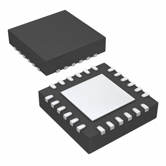
24-pin TSSOP (7.80 mm × 4.40 mm) and 24-pin
QFN (4.00 mm × 4.00 mm) package
The TS3A27518E-Q1 allows any SD, SDIO, and
multimedia card host controllers to be expanded out
to multiple cards or peripherals because the SDIO
interface consists of 6-bits: CMD, CLK, and Data[0:3]
signals. The TS3A27518E-Q1 has two control pins
that give additional flexibility to the user, for example,
the ability to mux two different audio-video signals
in equipment such as an LCD television, an LCD
monitor, or a notebook docking station.
Package Information(1)
PART NUMBER
2 Applications
•
•
•
TS3A27518E-Q1
SD/SDIO and MMC two port MUX
PC VGA video MUX/video systems
Audio and video signal routing
(1)
PACKAGE
BODY SIZE (NOM)
RTW (WQFN, 24)
4.00 mm × 4.00 mm
PW (TSSOP, 24)
7.80 mm × 4.40 mm
For all available packages, see the orderable addendum at
the end of the data sheet.
VCC
IN1
EN
Logic
IN2
NC1
NO1
NC4
COM1
NO4
COM4
NC2
NO2
NC5
COM2
NO5
COM5
NC3
NO3
COM3
NC6
NO6
COM6
GND
Copyright © 2016, Texas Instruments Incorporated
Functional Block Diagram
An IMPORTANT NOTICE at the end of this data sheet addresses availability, warranty, changes, use in safety-critical applications,
intellectual property matters and other important disclaimers. PRODUCTION DATA.
�TS3A27518E-Q1
www.ti.com
SCDS311D – JANUARY 2010 – REVISED OCTOBER 2022
Table of Contents
1 Features............................................................................1
2 Applications..................................................................... 1
3 Description.......................................................................1
4 Revision History.............................................................. 2
5 Pin Configuration and Functions...................................3
6 Specifications.................................................................. 4
6.1 Absolute Maximum Ratings........................................ 4
6.2 ESD Ratings............................................................... 4
6.3 Recommended Operating Conditions.........................4
6.4 Thermal Information....................................................5
6.5 Electrical Characteristics for 3.3-V Supply .................5
6.6 Electrical Characteristics for 2.5-V Supply .................7
6.7 Electrical Characteristics for 1.8-V Supply .................9
6.8 Typical Characteristics.............................................. 11
7 Parameter Measurement Information.......................... 14
8 Detailed Description......................................................19
8.1 Overview................................................................... 19
8.2 Functional Block Diagram......................................... 19
8.3 Feature Description...................................................19
8.4 Device Functional Modes..........................................19
9 Application and Implementation.................................. 20
9.1 Application Information............................................. 20
9.2 Typical Application.................................................... 20
10 Power Supply Recommendations..............................21
11 Layout........................................................................... 22
11.1 Layout Guidelines................................................... 22
11.2 Layout Example...................................................... 22
12 Device and Documentation Support..........................23
12.1 Documentation Support.......................................... 23
12.2 Receiving Notification of Documentation Updates..23
12.3 Support Resources................................................. 23
12.4 Trademarks............................................................. 23
12.5 Electrostatic Discharge Caution..............................23
12.6 Glossary..................................................................23
13 Mechanical, Packaging, and Orderable
Information.................................................................... 23
4 Revision History
NOTE: Page numbers for previous revisions may differ from page numbers in the current version.
Changes from Revision C (January 2019) to Revision D (November 2022)
Page
• Updated the numbering format for tables, figures, and cross-references throughout the document..................1
• Added functional safety-capable information to the Features section................................................................ 1
Changes from Revision B (May 2012) to Revision C (January 2019)
Page
• Added Device Information table, ESD Ratings table, Recommended Operating Conditions table, Feature
Description section, Device Functional Modes, Application and Implementation section, Power Supply
Recommendations section, Layout section, Device and Documentation Support section, and Mechanical,
Packaging, and Orderable Information section ..................................................................................................1
• Updated the numbering format for tables, figures, and cross-references throughout the document..................1
Changes from Revision A (March 2012) to Revision B (May 2012)
Page
• Changed device temp grade from 1 to 2, removed maximum withstand voltage info, changed C3B2 to C3B.. 1
• Added extra row to ordering information table....................................................................................................1
• Changed TA = –40°C to 85°C to TA = –40°C to 105°C.......................................................................................5
• Changed Full to –40°C to 85°C and added extra row with 85°C to 105°C and limits -7.5 to 7.5........................5
• Changed Full to –40°C to 85°C and added extra row with 85°C to 105°C with limits 68................................... 5
• Changed Full to –40°C to 85°C and added extra row with 85°C to 105°C with limits 70................................... 5
• Changed Full to –40°C to 85°C and added extra row with 85°C to 105°C with limits 5 µA................................ 5
• Changed TA = –40°C to 85°C to TA = –40°C to 105°C.......................................................................................7
• Changed Full to –40°C to 85°C and added extra row with 85°C to 105°C with limits 38.4................................ 7
• Changed Full to –40°C to 85°C and added extra row with 85°C to 105°C with limits 3..................................... 7
• Changed TA = –40°C to 85°C to TA = –40°C to 105°C.......................................................................................9
• Changed Full to –40°C to 85°C and added extra row with 85°C to 105°C and limits –5.8 to 5.8.......................9
• Changed Full to –40°C to 85°C and added extra row with 85°C to 105°C with limits 35.2................................ 9
• Changed Full to –40°C to 85°C and added extra row with 85°C to 105°C with limits 2.5.................................. 9
2
Submit Document Feedback
Copyright © 2022 Texas Instruments Incorporated
Product Folder Links: TS3A27518E-Q1
�TS3A27518E-Q1
www.ti.com
SCDS311D – JANUARY 2010 – REVISED OCTOBER 2022
20
NC6
19
NC3
IN1
21
NC2
22
NC1
23
24
N.C.
5 Pin Configuration and Functions
CO M1
1
18
NC4
GND
2
17
EN
CO M2
3
16
NC5
15
NO5
NC2
1
24
IN1
NC1
2
23
NC3
N.C.
3
22
NC6
CO M1
4
21
NC4
GND
5
20
EN
CO M2
6
19
NC5
CO M3
7
18
NO5
VCC
8
17
NO4
CO M4
9
16
NO6
CO M5
10
15
NO3
NO1
11
14
IN2
CO M6
12
13
NO2
Th ermal
CO M3
Pad
4
6
13
NO6
NO3
11
IN2
NO2
CO M6
NO1
CO M5
12
CO M4
10
NO4
9
14
8
5
7
VCC
No t to scale
Figure 5-1. RTW Package, 24-Pin WQFN (Top View)
No t to scale
Figure 5-2. PW Package, 24-Pin TSSOP (Top View)
Table 5-1. Pin Functions
PIN
NAME
TYPE(1)
DESCRIPTION
RTW
PW
COM1
1
4
I/O
Common-signal path
COM2
3
6
I/O
Common-signal path
COM3
4
7
I/O
Common-signal path
COM4
6
9
I/O
Common-signal path
COM5
7
10
I/O
Common-signal path
COM6
9
12
I/O
Common-signal path
EN
17
20
I
GND
2
5
—
IN1
21
24
I
Digital control to connect COM to NC or NO
IN2
11
14
I
Digital control to connect COM to NC or NO
N.C.
24
3
—
Not connected
NC1
23
2
I/O
Normally closed-signal path
NC2
22
1
I/O
Normally closed-signal path
NC3
20
23
I/O
Normally closed-signal path
NC4
18
21
I/O
Normally closed-signal path
NC5
16
19
I/O
Normally closed-signal path
NC6
19
22
I/O
Normally closed-signal path
NO1
8
11
I/O
Normally open-signal path
NO2
10
13
I/O
Normally open-signal path
NO3
12
15
I/O
Normally open-signal path
NO4
14
17
I/O
Normally open-signal path
NO5
15
18
I/O
Normally open-signal path
NO6
13
16
I/O
Normally open-signal path
VCC
5
8
—
Voltage supply
(1)
Digital control to enable or disable all signal paths
Ground.
I = input, O = output
Submit Document Feedback
Copyright © 2022 Texas Instruments Incorporated
Product Folder Links: TS3A27518E-Q1
3
�TS3A27518E-Q1
www.ti.com
SCDS311D – JANUARY 2010 – REVISED OCTOBER 2022
6 Specifications
6.1 Absolute Maximum Ratings
over operating free-air temperature range (unless otherwise noted)(1)
range(2)
MIN
MAX
–0.5
4.6
V
–0.5
4.6
V
V+
Supply voltage
VNC
VNO
VCOM
Analog voltage range(2) (3) (4)
IK
Analog port diode current(5)
V+ < VNC, VNO, VCOM < 0
–50
INC
INO
ICOM
ON-state switch current(6)
VNC, VNO, VCOM = 0 to V+
–50
50
VI
Digital input voltage range(2) (3)
–0.5
4.6
IIK
Digital input clamp current(2) (3)
I+
Continuous current through V+
IGND
Continuous current through GND
Tstg
Storage temperature range
(1)
(2)
(3)
(4)
(5)
(6)
VIO < VI < 0
UNIT
mA
mA
V
–50
mA
100
mA
–100
mA
–65
150
°C
Stresses beyond those listed under Absolute Maximum Ratings may cause permanent damage to the device. These are stress
ratings only, which do not imply functional operation of the device at these or any other conditions beyond those indicated under
Recommended Operating Conditions. Exposure to absolute-maximum-rated conditions for extended periods may affect device
reliability.
All voltages are with respect to ground, unless otherwise specified.
The input and output voltage ratings may be exceeded if the input and output clamp-current ratings are observed.
This value is limited to 5.5 V maximum.
Requires clamp diodes on analog port to V+.
Pulse at 1-ms duration


 工商网监
湘ICP备2023018690号
工商网监
湘ICP备2023018690号
