UCC27532-Q1
www.ti.com
SLVSCE4A – DECEMBER 2013 – REVISED JANUARY 2014
2.5-A and 5-A, 35-VMAX VDD FET and IGBT Single-Gate Driver
FEATURES
1
•
•
•
•
•
•
•
•
•
•
•
•
•
•
•
•
•
Qualified for Automotive Applications
AEC-Q100 Qualified With the Following
Results:
– Device Temperature Grade 1
– Device HBM ESD Classification Level H2
– Device CDM ESD Classification Level C4B
Low-Cost Gate Driver (offering optimal
solution for driving FET and IGBTs)
Superior Replacement to Discrete Transistor
Pair Drive (providing easy interface with
controller)
CMOS Compatible Input-Logic Threshold
(becomes fixed at VDD above 18 V)
Split Outputs Allow Separate Turnon and
Turnoff Tuning
Enable with Fixed TTL Compatible Threshold
High 2.5-A Source and 5-A Sink Peak-Drive
Currents at 18-V VDD
Wide VDD Range From 10 V up to 35 V
Input Pins Capable of Withstanding up to –5-V
DC Below Ground
Output Held Low When Inputs are Floating or
During VDD UVLO
Fast Propagation Delays (17-ns typical)
Fast Rise and Fall Times
(15-ns and 7-ns typical with 1800-pF Load)
Undervoltage Lockout (UVLO)
Used as a High-Side or Low-Side Driver (if
designed with proper bias and signal isolation)
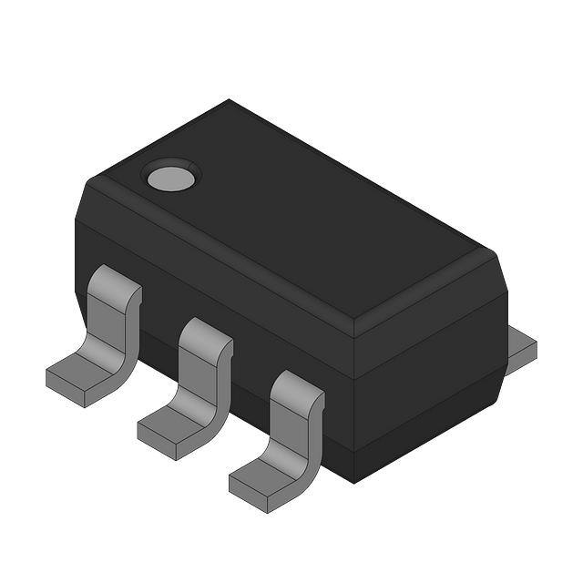
Low-Cost Space-Saving 6-Pin DBV (SOT-23)
Package
Operating Temperature Range of –40°C to
140°C
APPLICATIONS
•
•
•
•
•
•
Automotive
Switch-Mode Power Supplies
DC-to-DC Converters
Solar Inverters, Motor Control, UPS
HEV and EV Chargers
Home Appliances
•
•
Renewable Energy Power Conversion
SiC FET Converters
DESCRIPTION
The UCC27532-Q1 device is a single-channel highspeed gate driver capable of effectively driving
MOSFET and IGBT power switches by up to 2.5-A
source and 5-A sink (asymmetrical drive) peak
current. Strong sink capability in asymmetrical drive
boosts immunity against parasitic Miller turnon effect.
The UCC27532-Q1 device also features a split-output
configuration where the gate-drive current is sourced
through the OUTH pin and sunk through the OUTL
pin. This pin arrangement allows the user to apply
independent turnon and turnoff resistors to the OUTH
and OUTL pins respectively and easily control the
switching slew rates.
The driver has rail-to-rail drive capability and an
extremely-small propagation delay of 17 ns (typically).
The UCC27532-Q1 device has a CMOS-input
threshold-centered 55% rise and 45% fall in regards
of VDD at VDD below or equal 18 V. When VDD is
above 18 V, the input threshold remains fixed at the
maximum level.
The driver has an EN pin with a fixed TTL-compatible
threshold. EN is internally pulled up; pulling EN low
disables driver, while leaving it open provides normal
operation. The EN pin can be used as an additional
input with the same performance as the IN pin.
Leaving the input pin of driver open holds the output
low. The logic behavior of the driver is shown in the
Timing Diagram, Input/Output Logic Truth Table, and
Typical Application Diagrams.
Internal circuitry on the VDD pin provides an
undervoltage-lockout function that holds the output
low until the VDD supply voltage is within operating
range.
The UCC27532-Q1 driver is offered in a 6-pin
standard SOT-23 (DBV) package. The device
operates over a wide temperature range of –40°C to
140°C.
EN
1
6 OUTH
IN
2
5 OUTL
VDD
3
4 GND
1
Please be aware that an important notice concerning availability, standard warranty, and use in critical applications of
Texas Instruments semiconductor products and disclaimers thereto appears at the end of this data sheet.
PRODUCTION DATA information is current as of publication date.
Products conform to specifications per the terms of the Texas
Instruments standard warranty. Production processing does not
necessarily include testing of all parameters.
Copyright © 2013–2014, Texas Instruments Incorporated
�UCC27532-Q1
SLVSCE4A – DECEMBER 2013 – REVISED JANUARY 2014
www.ti.com
This integrated circuit can be damaged by ESD. Texas Instruments recommends that all integrated circuits be handled with
appropriate precautions. Failure to observe proper handling and installation procedures can cause damage.
ESD damage can range from subtle performance degradation to complete device failure. Precision integrated circuits may be more
susceptible to damage because very small parametric changes could cause the device not to meet its published specifications.
ABSOLUTE MAXIMUM RATINGS (1) (2) (3)
over operating free-air temperature range (unless otherwise noted)
MIN
MAX
Supply voltage range
VDD
–0.3
35
Continuous
OUTH, OUTL
–0.3
VDD +0.3
Pulse
OUTH, OUTL (200 ns)
–2
VDD +0.3
–5
27
–6.5
27
Continuous IN, EN
Pulse IN, EN (1.5 µs)
Electrostatic discharge (ESD) rating
Human body model (HBM)
Charged device model (CDM)
kV
V
150
Storage temperature range, Tstg
–65
150
(2)
(3)
V
2
–40
(1)
V
750
Operating virtual junction temperature range, TJ
Lead temperature
UNIT
Soldering, 10 seconds
300
Reflow
260
°C
Stresses beyond those listed under absolute maximum ratings may cause permanent damage to the device. These are stress ratings
only and functional operation of the device at these or any other conditions beyond those indicated under recommended operating
conditions is not implied. Exposure to absolute-maximum-rated conditions for extended periods may affect device reliability.
All voltages are with respect to GND unless otherwise noted. Currents are positive into, negative out of the specified terminal. See
Packaging Section of the datasheet for thermal limitations and considerations of packages.
These devices are sensitive to electrostatic discharge; follow proper device handling procedures.
THERMAL INFORMATION
UCC27532-Q1
THERMAL METRIC
(1)
DBV
UNIT
6 PINS
θJA
Junction-to-ambient thermal resistance
178.3
θJCtop
Junction-to-case (top) thermal resistance
109.7
θJB
Junction-to-board thermal resistance
28.3
ψJT
Junction-to-top characterization parameter
14.7
ψJB
Junction-to-board characterization parameter
27.8
θJCbot
Junction-to-case (bottom) thermal resistance
n/a
(1)
°C/W
For more information about traditional and new thermal metrics, see the IC Package Thermal Metrics application report, SPRA953.
RECOMMENDED OPERATING CONDITIONS
over operating free-air temperature range (unless otherwise noted)
MIN
TYP
MAX
10
18
32
V
–40
140
°C
Input voltage, IN
–5
25
Enable, EN
–5
25
Supply voltage range, VDD
Operating junction temperature range
2
Submit Documentation Feedback
UNIT
V
Copyright © 2013–2014, Texas Instruments Incorporated
Product Folder Links :UCC27532-Q1
�UCC27532-Q1
www.ti.com
SLVSCE4A – DECEMBER 2013 – REVISED JANUARY 2014
ELECTRICAL CHARACTERISTICS
Unless otherwise noted, VDD = 18 V, TA = TJ = –40°C to 140°C, IN switching from 0 V to VDD, 1-µF capacitor from VDD to
GND, ƒ = 100 kHz. Currents are positive into and negative out of the specified terminal. OUTH and OUTL are tied together.
Typical condition specifications are at 25°C.
PARAMETER
CONDITION
MIN
TYP
MAX
IN, EN = VDD
100
240
350
IN, EN = GND
100
250
350
8
8.9
9.8
7.3
8.2
9.1
UNIT
Bias Currents
IDDoff
Startup current, VDD = 7.0
μA
Under Voltage Lockout (UVLO)
VON
Supply start threshold
VOFF
Minimum operating voltage after
supply start
VDD_H
Supply voltage hysteresis
V
0.7
Input (IN)
VIN_H
Input signal high threshold
Output high
8.8
9.4
10
VIN_L
Input signal low threshold
Output low
6.7
7.3
7.9
VIN_HYS
Input signal hysteresis
V
2.1
Enable (EN)
VEN_H
Enable signal high threshold
Output high
1.7
1.9
2.1
VEN_L
Enable signal low threshold
Output low
0.8
1
1.2
VEN_HY
Enable signal hysteresis
V
0.9
S
Outputs (OUTH/OUTL)
ISRC/SNK
Source peak current (OUTH)/ sink
peak current (OUTL) (1)
CLOAD = 0.22 µF, ƒ = 1 kHz
VOH
OUTH, high voltage
IOUTH = –10 mA
VOL
OUTL, low voltage
IOUTL = 100 mA
ROH
OUTH, pull-up resistance (2)
ROL
OUTL, pull-down resistance
Switching Time
TA = 25°C, IOUT = -10 mA
TA = –40°C to 140°C, IOUT = -10 mA
TA = 25°C, IOUT = 100 mA
TA = –40°C to 140°C, IOUT = 100 mA
–2.5 / +5
VDD –0.2
11
A
VDD –0.12 VDD –0.07
0.065
0.125
12
12.5
7
12
20
0.45
0.65
0.85
0.3
0.65
1.25
Rise time
CLOAD = 1.8 nF
15
tF
Fall time
CLOAD = 1.8 nF
7
tD1
Turnon propagation delay
CLOAD = 1.8 nF, IN = 0 V to VDD
17
26
tD2
Turnoff propagation delay
CLOAD = 1.8 nF, IN = VDD to 0 V
17
26
(3)
Ω
(1) (3)
tR
(1)
(2)
V
ns
Ensured by design and tested during characterization. Not production tested.
Output pullup resistance here is a DC measurement that measures resistance of PMOS structure only, not N-channel structure. The
effective dynamic pull-up resistance is 3 × ROL.
See Figure 1.
Submit Documentation Feedback
Copyright © 2013–2014, Texas Instruments Incorporated
Product Folder Links :UCC27532-Q1
3
�UCC27532-Q1
SLVSCE4A – DECEMBER 2013 – REVISED JANUARY 2014
www.ti.com
Timing Diagram
High
INPUT
Low
90%
OUTPUT
10%
tD1 tR
tD2 tF
Figure 1. (OUTH tied to OUTL)
Input = IN, Output = OUT (EN = VDD)
or Input = EN, Output = OUT (IN = VDD)
4
Submit Documentation Feedback
Copyright © 2013–2014, Texas Instruments Incorporated
Product Folder Links :UCC27532-Q1
�UCC27532-Q1
www.ti.com
SLVSCE4A – DECEMBER 2013 – REVISED JANUARY 2014
DEVICE INFORMATION
SOT-23 PACKAGE
6-PIN DBV
(TOP VIEW)
EN
1
6 OUTH
IN
2
5 OUTL
VDD
3
4 GND
TERMINAL FUNCTIONS
TERMINAL
I/O
FUNCTION
NAME
PIN NUMBER
EN
1
I
Enable
(Pull EN to GND in order to disable output, pull it high or leave it open to enable the
output)
GND
4
–
Ground (all signals are referenced to this node)
IN
2
I
Driver non-inverting input (CMOS threshold)
OUTL
5
O
5-A sink current output of driver
OUTH
6
O
2.5-A source current output of driver
VDD
3
I
Bias supply input
INPUT/OUTPUT LOGIC TRUTH TABLE
EN PIN
OUTH PIN
OUTL PIN
OUT
(OUTH and OUTL pins
tied together)
L
L
High-impedance
L
L
L
H
High-impedance
L
L
H
L
High-impedance
L
L
H
H
H
High-impedance
H
IN PIN
Block Diagram
(EN Pullup Resistance to Vref = 500 kΩ, Vref = 5.8 V, In Pulldown Resistance to GND = 230 kΩ)
IN
VDD
2
Vref
EN
1
3
VDD
6
OUTH
5
OUTL
VDD
GND
4
UVLO
Submit Documentation Feedback
Copyright © 2013–2014, Texas Instruments Incorporated
Product Folder Links :UCC27532-Q1
5
�UCC27532-Q1
SLVSCE4A – DECEMBER 2013 – REVISED JANUARY 2014
www.ti.com
Typical Application Diagrams
UCC27532-Q1
EN
1
OUTH
6
IN
OUTL
+
2
5
VDD
GND
3
+
–
4
GND
Bouncing Up
to – 6.5 V
18 V
ISENSE
Controller
+
–
VCE(sense)
VCC
Figure 2. Driving IGBT Without Negative Bias
UCC27532-Q1
EN
OUTH
1
IN
6
OUTL
+
2
5
3
4
VDD
+
–
GND
18 V
+
–
13 V
Figure 3. Driving IGBT With 13-V Negative Turnoff Bias
6
Submit Documentation Feedback
Copyright © 2013–2014, Texas Instruments Incorporated
Product Folder Links :UCC27532-Q1
�UCC27532-Q1
www.ti.com
SLVSCE4A – DECEMBER 2013 – REVISED JANUARY 2014
E/2
+
–
Isolated
UCC27532-Q1
Isolated
.
UCC27532-Q1
Controller
Isolated
UCC27532-Q1
Isolated
UCC27532-Q1
E/2
+
–
Figure 4. Using UCC27532-Q1 Drivers in an Inverter
Submit Documentation Feedback
Copyright © 2013–2014, Texas Instruments Incorporated
Product Folder Links :UCC27532-Q1
7
�UCC27532-Q1
SLVSCE4A – DECEMBER 2013 – REVISED JANUARY 2014
www.ti.com
TYPICAL CHARACTERISTICS
RISE TIME
vs
SUPPLY VOLTAGE
FALL TIME
vs
SUPPLY VOLTAGE
12
25
10
Fall Time (ns)
Rise Time (ns)
20
15
10
8
6
4
Cload = 1.8nF
Cload = 1.8nF
2
5
0
10
20
30
10
30
Figure 6.
PROPAGATION DELAY
vs
SUPPLY VOLTAGE
OPERATING SUPPLY CURRENT
vs
FREQUENCY
30
40
C002
Figure 5.
21
VDD = 10V
TurnOn
VDD = 18V
VDD = 32V
25
TurnOff
19
20
Supply Voltage (V)
C001
Supply Current (mA)
Input To Output Propagation Delay (ns)
Supply Voltage (V)
0
40
17
15
20
15
10
5
0
10
20
Supply Voltage (V)
30
40
Cload = 1.8nF
C003
0
0
100
200
300
400
500
Frequency (kHz)
C001
Figure 7.
8
Figure 8.
Submit Documentation Feedback
Copyright © 2013–2014, Texas Instruments Incorporated
Product Folder Links :UCC27532-Q1
�UCC27532-Q1
www.ti.com
SLVSCE4A – DECEMBER 2013 – REVISED JANUARY 2014
TYPICAL CHARACTERISTICS (continued)
START-UP CURRENT
vs
TEMPERATURE
OPERATING SUPPLY CURRENT
vs
TEMPERATURE (OUTPUT SWITCHING)
350
4.5
EN = IN = Vdd
EN = IN = GND
4.3
4.1
Idd (mA)
Startup Current (µA)
300
250
3.9
200
3.7
Vdd = 18V
Cload = 1.8nF
fsw = 100kHz
Vdd = 7V
150
-50
0
50
100
3.5
150
-50
0
Temperature (Ü&�
50
100
150
7HPSHUDWXUH��Û&�
C003
C006
Figure 9.
Figure 10.
UVLO THRESHOLD VOLTAGE
vs
TEMPERATURE
INPUT THRESHOLD
vs
TEMPERATURE
12
9.6
UVLO Rising
Turn-On
UVLO Falling
Turn-Off
11
Input Threshold (V)
Vdd UVLO Threshold (V)
9.2
8.8
10
9
8
8.4
7
6
8
-50
0
50
100
150
-50
0
50
100
150
Temperature ( Ü&�
7HPSHUDWXUH��Û&�
C002
C007
Figure 11.
Figure 12.
Submit Documentation Feedback
Copyright © 2013–2014, Texas Instruments Incorporated
Product Folder Links :UCC27532-Q1
9
�UCC27532-Q1
SLVSCE4A – DECEMBER 2013 – REVISED JANUARY 2014
www.ti.com
TYPICAL CHARACTERISTICS (continued)
ENABLE THRESHOLD
vs
TEMPERATURE
OUTPUT PULLUP RESISTANCE
vs
TEMPERATURE
2.4
25
Enable
Disable
2.2
ROH
20
Output Pull-Up Resistance ()
Enable Threshold (V)
2
1.8
1.6
1.4
1.2
15
10
1
Vdd = 18V
0.8
-50
0
50
100
150
5
-50
7HPSHUDWXUH��Û&�
0
50
100
150
7HPSHUDWXUH��Û&�
C009
C010
Figure 13.
Figure 14.
OUTPUT PULLDOWN RESISTANCE
vs
TEMPERATURE
OPERATING SUPPLY CURRENT
vs
TEMPERATURE (OUTPUT IN DC ON AND OFF CONDITION)
1.2
0.6
IN=HIGH
ROL
IN=LOW
Operating Supply Current (mA)
Output Pull-Down Resistance ()
1
0.8
0.6
0.5
0.4
0.3
0.4
Vdd = 18V
Vdd = 18V
0.2
0.2
-50
0
50
100
150
-50
0
50
150
C012
C011
Figure 15.
10
100
7HPSHUDWXUH��Û&�
7HPSHUDWXUH��Û&�
Figure 16.
Submit Documentation Feedback
Copyright © 2013–2014, Texas Instruments Incorporated
Product Folder Links :UCC27532-Q1
�UCC27532-Q1
www.ti.com
SLVSCE4A – DECEMBER 2013 – REVISED JANUARY 2014
TYPICAL CHARACTERISTICS (continued)
INPUT-TO-OUTPUT PROPAGATION DELAY
vs
TEMPERATURE
RISE TIME
vs
TEMPERATURE
16
30
Turn-On
Turn-Off
15
Rise Time (ns)
Propagation Delay (ns)
25
20
14
13
Vdd = 18V
Cload = 1.8nF
15
12
Vdd = 18V
10
11
-50
0
50
100
-50
150
0
7HPSHUDWXUH��Û&�
50
100
C013
C014
Figure 17.
Figure 18.
FALL TIME
vs
TEMPERATURE
OPERATING SUPPLY CURRENT
vs
SUPPLY VOLTAGE (OUTPUT SWITCHING)
9
10
8
8
Supply Current (mA)
Fall Time (ns)
150
7HPSHUDWXUH��Û&�
7
6
Vdd = 18V
Cload = 1.8nF
6
4
Cload = 10nF
fsw = 20kHz
5
2
4
0
-50
0
50
100
150
0
7HPSHUDWXUH��Û&�
10
20
30
40
Supply Voltage (V)
C015
Figure 19.
C016
Figure 20.
Submit Documentation Feedback
Copyright © 2013–2014, Texas Instruments Incorporated
Product Folder Links :UCC27532-Q1
11
�UCC27532-Q1
SLVSCE4A – DECEMBER 2013 – REVISED JANUARY 2014
www.ti.com
TYPICAL CHARACTERISTICS (continued)
RISE TIME
vs
SUPPLY VOLTAGE
FALL TIME
vs
SUPPLY VOLTAGE
70
140
60
120
Fall Time (ns)
Rise Time (ns)
50
100
80
40
30
60
20
Cload = 10nF
Cload = 10nF
40
10
0
10
20
30
40
0
Supply Voltage (V)
10
20
C017
Figure 21.
12
30
40
Supply Voltage (V)
C018
Figure 22.
Submit Documentation Feedback
Copyright © 2013–2014, Texas Instruments Incorporated
Product Folder Links :UCC27532-Q1
�UCC27532-Q1
www.ti.com
SLVSCE4A – DECEMBER 2013 – REVISED JANUARY 2014
APPLICATION INFORMATION
High-current gate driver devices are required in switching power applications for a variety of reasons. In order to
enable fast switching of power devices and reduce associated switching power losses, a powerful gate driver can
be used between the PWM output of controllers or signal isolation devices and the gates of the power
semiconductor devices. Further, gate drivers are indispensable when having the PWM controller directly drive the
gates of the switching devices is not feasible. This situation is often encountered because the PWM signal from a
digital controller or signal isolation device is often a 3.3-V or 5-V logic signal which is not capable of effectively
turning on a power switch. A level shifting circuitry is required to boost the logic-level signal to the gate-drive
voltage in order to fully turn on the power device and minimize conduction losses. Traditional buffer drive circuits
based on NPN and PNP bipolar (or P-channel and N-channel MOSFET) transistors in totem-pole arrangement,
being emitter-follower configurations, prove inadequate for this function because these circuits lack level-shifting
capability and low-drive voltage protection. Gate drivers effectively combine both the level-shifting, buffer drive,
and UVLO functions. Gate drivers have other uses such as minimizing the effect of switching noise by locating
the high-current driver physically close to the power switch, driving gate-drive transformers, controlling floating
power device gates, and reducing power dissipation and thermal stress in controllers by moving gate charge
power losses into itself.
The UCC27532-Q1 device is very flexible in this role with a strong current-drive capability and wide supplyvoltage range up to 35 V. These features allow the driver to be used in 12-V Si MOSFET applications, 20-V and
–5-V (relative to source) SiC FET applications, 15-V and –15-V (relative to emitter) IGBT applications, and many
others. As a single-channel driver, the UCC27532-Q1 device can be used as a low-side or high-side driver. To
use the device as a low-side driver, the switch ground is typically the system ground so it can be connected
directly to the gate driver. To use as a high-side driver with a floating return node, however, signal isolation is
required from the controller as well as an isolated bias to the UCC27532-Q1 device. Alternatively, in a high-side
drive configuration the UCC27532-Q1 device can be tied directly to the controller signal and biased with a nonisolated supply. However, in this configuration the outputs of the UCC27532-Q1 device must drive a pulse
transformer which then drives the power-switch to work properly with the floating source and emitter of the power
switch. Further, having the ability to control turnon and turnoff speeds independently with both the OUTH and
OUTL pins ensures optimum efficiency while maintaining system reliability. These requirements coupled with the
need for low propagation delays and availability in compact, low-inductance packages with good thermal
capability makes gate driver devices such as the UCC27532-Q1 device extremely important components in
switching power combining benefits of high-performance, low cost, component count and board-space reduction,
and simplified system design.
Table 1. UCC27532-Q1 Features and Benefits
FEATURE
BENEFIT
High source and sink current capability, 2.5 A and
5 A (asymmetrical).
High current capability offers flexibility in employing UCC27532-Q1 device device to
drive a variety of power switching devices at varying speeds.
Low 17 ns (typ) propagation delay.
Extremely low pulse transmission distortion.
Wide VDD operating range of 10 V to 32 V.
Flexibility in system design.
Can be used in split-rail systems such as driving IGBTs with both positive and
negative (relative to Emitter) supplies.
Optimal for many SiC FETs.
VDD UVLO protection.
Outputs are held Low in UVLO condition, which ensures predictable, glitch-free
operation at power-up and power-down.
High UVLO of 8.9 V typical ensures that power switch is not on in high-impedance
state which could result in high power dissipation or even failures.
Outputs held low when input pin (IN) in floating
condition.
Safety feature, especially useful in passing abnormal condition tests during safety
certification
Split output structure (OUTH, OUTL).
Allows independent optimization of turnon and turnoff speeds using series gate
resistors.
Strong sink current (5 A) and low pulldown
impedance (0.65 Ω).
High immunity to high dV/dt Miller turnon events.
CMOS compatible input threshold logic with wide
2.1-V hysteresis.
Excellent noise immunity.
Input capable of withstanding –6.5 V.
Enhanced signal reliability in noisy environments that experience ground bounce on
the gate driver.
Submit Documentation Feedback
Copyright © 2013–2014, Texas Instruments Incorporated
Product Folder Links :UCC27532-Q1
13
�UCC27532-Q1
SLVSCE4A – DECEMBER 2013 – REVISED JANUARY 2014
www.ti.com
VDD Under Voltage Lockout
The UCC27532-Q1 device has an internal undervoltage-lockout (UVLO) protection feature on the VDD-pin
supply-circuit blocks. To ensure acceptable power dissipation in the power switch, this UVLO prevents the
operation of the gate driver at low supply voltages. Whenever the driver is in UVLO condition (when the VDD
voltage less than VON during power-up and when the VDD voltage is less than VOFF during power down), this
circuit holds all outputs LOW, regardless of the status of the inputs. The UVLO is typically 8.9 V with a 700-mV
typical hysteresis. This hysteresis helps prevent chatter when low-VDD supply voltages have noise from the
power supply. This hysteresis also prevents chatter when there are droops in the VDD bias voltage when the
system commences switching and there is a sudden increase in IDD. The capability to operate at voltage levels
such as 10 V to 32 V provides flexibility to drive Si MOSFETs, IGBTs, and emerging SiC FETs.
VDD Threshold
VDD
IN
OUT
Figure 23. Power Up
Input Stage
The input pin of UCC27532-Q1 device is based on a standard CMOS-compatible input-threshold logic that is
dependent on the VDD supply voltage. The input threshold is approximately 55% of VDD for rise and 45% of
VDD for fall. With 18-V VDD, the typical high threshold is 9.4 V and the typical low threshold is 7.3 V. The 2.1-V
hysteresis offers excellent noise immunity compared to traditional TTL logic implementations where the
hysteresis is typically less than 0.5 V. For proper operation using CMOS input, the input signal level must be at a
voltage equal to VDD. Using an input signal slightly larger than the threshold but less than VDD for the CMOS
input can result in slower propagation delay from input to output (for example). This device also features tight
control of the input-pin threshold voltage levels which eases system design considerations and ensures stable
operation across temperature. The very low input capacitance, typically 20 pF, on these pins reduces loading
and increases switching speed.
The device features an important safety function where the output is held in the low state whenever the input pin
is in a floating condition. This function is achieved using GND pulldown resistors on the non-inverting input pin
(IN pin), as shown in the Block Diagram.
The input stage of the driver is best driven by a signal with a short rise or fall time. Caution must be exercised
whenever the driver is used with slowly varying input signals, especially in situations where the device is located
in a separate daughter board or PCB layout has long input-connection traces:
• High dI/dt current from the driver output coupled with board layout parasitics can cause ground bounce.
Because the device features just one GND pin which can be referenced to the power ground, this can
interfere with the differential voltage between input pins and GND and can trigger an unintended change of
output state. Because of the fast 17-ns propagation delay, this can ultimately result in high-frequency
oscillations, which increases power dissipation and poses a risk of damage
• 2.1-V input threshold hysteresis boosts noise immunity compared to most other industry standard drivers.
14
Submit Documentation Feedback
Copyright © 2013–2014, Texas Instruments Incorporated
Product Folder Links :UCC27532-Q1
�UCC27532-Q1
www.ti.com
SLVSCE4A – DECEMBER 2013 – REVISED JANUARY 2014
If limiting the rise or fall times to the power device in order to reduce EMI is necessary, then an external
resistance is highly recommended between the output of the driver and the power device instead of adding
delays on the input signal. This external resistor has the additional benefit of reducing part of the gate-chargerelated power dissipation in the gate-driver device package and transferring the dissipation into the external
resistor itself.
Enable Function
The enable (EN) pin of the UCC27532-Q1 device has an internal pullup resistor to an internal reference voltage.
Therefore, leaving the EN pin floating turns on the driver and allows it to send output signals properly. If desired,
the EN pin can also be driven by low-voltage logic to enable and disable the driver.
Output Stage
Figure 24 shows the output stage of the UCC27532-Q1 device. The UCC27532-Q1 device features a unique
architecture on the output stage which delivers the highest peak-source current when it is most needed during
the Miller plateau region of the power switch turnon transition (when the power switch drain or collector voltage
experiences dV/dt). The device output stage features a hybrid pullup structure using a parallel arrangement of NChannel and P-Channel MOSFET devices. By turning on the N-Channel MOSFET during a narrow instant when
the output changes state from low to high, the gate driver device is able to deliver a brief boost in the peak
sourcing current enabling fast turn on.
VDD
R OH
R NMOS, Pull Up
OUTH
Input Signal Anti Shoot Through
Circuitry
Narrow Pulse at
each Turn On
OUTL
R OL
Figure 24. UCC27532-Q1 Gate-Driver Output Stage
The ROH parameter (see ELECTRICAL CHARACTERISTICS) is a DC measurement and is representative of the
on-resistance of the P-Channel device only because the N-Channel device is turned-on only during output
change of state from low to high. Thus the effective resistance of the hybrid pullup stage is much lower than what
is represented by ROH parameter. The pulldown structure is composed of a N-Channel MOSFET only. The ROL
parameter (see ELECTRICAL CHARACTERISTICS), which is also a DC measurement, is representative of true
impedance of the pulldown stage in the device. In UCC27532-Q1 device, the effective resistance of the hybrid
pullup structure is approximately 3 × ROL.
The UCC27532-Q1 device is capable of delivering 2.5-A source, 5-A Sink (asymmetrical drive) at VDD = 18 V.
Strong sink capability in asymmetrical drive results in a very low pulldown impedance in the driver output stage
which boosts immunity against the parasitic Miller turnon (high slew-rate dV/dt turn on) effect that is seen in both
IGBT and FET power switches.
Submit Documentation Feedback
Copyright © 2013–2014, Texas Instruments Incorporated
Product Folder Links :UCC27532-Q1
15
�UCC27532-Q1
SLVSCE4A – DECEMBER 2013 – REVISED JANUARY 2014
www.ti.com
An example of a situation where Miller turnon is a concern is synchronous rectification (SR). In SR application,
the dV/dt occurs on MOSFET drain when the MOSFET is already held in the off state by the gate driver. The
current charging the CGD Miller capacitance during this high dV/dt is shunted by the pulldown stage of the driver.
If the pulldown impedance is not low enough then a voltage spike can result in the VGS of the MOSFET, which
can result in spurious turnon. This phenomenon is illustrated in Figure 25.
VDS
VIN
Miller Turn -On Spike in V GS
C GD
Gate Driver
RG
COSS
ISNK
CGS
ROL
VTH
VGS of
MOSFET
ON OFF
VIN
VDS of
MOSFET
Figure 25. Low Pulldown Impedance in the UCC27532-Q1 Device
(Output Stage Mitigates Miller Turnon Effect)
The driver output voltage swings between VDD and GND providing rail-to-rail operation because of the MOS
output stage which delivers very low dropout. The presence of the MOSFET body diodes also offers low
impedance to switching overshoots and undershoots which means that in many cases, external Schottky diode
clamps can be eliminated.
Power Dissipation
Power dissipation of the gate driver has two portions as shown in Equation 1.
PDISS = PDC + PSW
(1)
The DC portion of the power dissipation is shown in Equation 2.
PDC = IQ ´ VDD
where
•
IQ is the quiescent current for the driver
(2)
The quiescent current is the current consumed by the device to bias all internal circuits such as input stage,
reference voltage, logic circuits, protections, and others, as well as any current associated with switching of
internal devices when the driver output changes state (such as charging and discharging of parasitic
capacitances and parasitic shoot-through). The UCC27532-Q1 device features very-low quiescent currents (less
than 1 mA) and contains internal logic to eliminate any shoot-through in the output driver stage. Thus the effect
of the PDC on the total power dissipation within the gate driver can be assumed as insignificant. In practice, this is
the power consumed by the driver when the output is disconnected from the gate of power switch.
The power dissipated in the gate driver package during switching (PSW) is based on the following factors:
• Gate charge required of the power device (typically a function of the drive voltage VG, which is very close to
input bias supply voltage VDD due to low VOH drop-out)
• Switching frequency
• Use of external gate resistors
16
Submit Documentation Feedback
Copyright © 2013–2014, Texas Instruments Incorporated
Product Folder Links :UCC27532-Q1
�UCC27532-Q1
www.ti.com
SLVSCE4A – DECEMBER 2013 – REVISED JANUARY 2014
When a driver device is tested with a discrete, capacitive load, calculating the power that is required from the
bias supply is simple. Equation 3 calculates the energy that must be transferred from the bias supply to charge
the capacitor.
1
EG = CLOAD VDD2
2
where
•
•
CLOAD is load capacitor
VDD is bias voltage feeding the driver
(3)
When the capacitor is discharged an equal amount of energy is dissipated. During turnoff the energy stored in
capacitor is fully dissipated in drive circuit which leads to a total power loss during switching cycle given by
Equation 4.
PG = CLOAD VDD2 ƒSW
where
•
ƒSW is the switching frequency
(4)
The switching load presented by a power FET and IGBT can be converted to an equivalent capacitance by
examining the gate charge required to switch the device. This gate charge includes the effects of the input
capacitance plus the added charge required to swing the drain voltage of the power device as it switches
between the ON and OFF states. Most manufacturers provide specifications of typical and maximum gate
charge, in nC, to switch the device under specified conditions. Using the gate charge Qg, the power that must be
dissipated when charging a capacitor is determined by using the equivalence, Qg = CLOADVDD, which results in
Equation 5 for power:
PG = CLOAD VDD2 ƒSW = Qg VDD ƒSW
(5)
This power, PG, is dissipated in the resistive elements of the circuit when the MOSFET and IGBT is turning on or
turning off. Half of the total power is dissipated when the load capacitor is charged during turnon, and the other
half is dissipated when the load capacitor is discharged during turnoff. When no external gate resistor is
employed between the driver and MOSFET and IGBT, this power is completely dissipated inside the driver
package. With the use of external gate drive resistors, the power dissipation is shared between the internal
resistance of driver and external gate resistor in accordance to the ratio of the resistances (more power is
dissipated in the higher resistance component). Based on this simplified analysis, the driver power dissipation
during switching is calculated in Equation 6.
æ
ö
ROFF
RON
PSW = 0.5 ´ Qg ´ VDD ´ ƒSW ç
+
÷
ç (ROFF + RGATE ) (RON + RGATE ) ÷
è
ø
where
•
•
ROFF = ROL
RON (effective resistance of pull-up structure) = 3 × ROL
(6)
Submit Documentation Feedback
Copyright © 2013–2014, Texas Instruments Incorporated
Product Folder Links :UCC27532-Q1
17
�UCC27532-Q1
SLVSCE4A – DECEMBER 2013 – REVISED JANUARY 2014
www.ti.com
Thermal Information
The useful range of a driver is greatly affected by the drive power requirements of the load and the thermal
characteristics of the package. In order for a gate driver to be useful over a particular temperature range the
package must allow for the efficient removal of the heat produced while keeping the junction temperature within
rated limits. The thermal metrics for the driver package is summarized in the THERMAL INFORMATION table.
For detailed information regarding the thermal information table, please see SPRA953.
PCB Layout
Proper PCB layout is extremely important in a high-current fast-switching circuit in order to provide appropriate
device operation and design robustness. The UCC27532-Q1 gate driver incorporates short propagation delays
and powerful output stages capable of delivering large current peaks with very fast rise and fall times at the gate
of power switch to facilitate voltage transitions very quickly. At higher VDD voltages, the peak current capability is
even higher (2.5-A and 5-A peak current is at VDD = 18 V). Very high di/dt can cause unacceptable ringing if the
trace lengths and impedances are not well controlled. The following circuit layout guidelines are strongly
recommended when designing with these high-speed drivers.
• Locate the driver device as close as possible to the power device in order to minimize the length of highcurrent traces between the driver output pins and the gate of the power-switch device.
• Locate the VDD bypass capacitors between VDD and GND as close as possible to the driver with minimal
trace length to improve the noise filtering. These capacitors support high peak current being drawn from VDD
during turnon of power switch. The use of low-inductance SMD components such as chip resistors and chip
capacitors is highly recommended.
• The turnon and turnoff current-loop paths (driver device, power switch, and VDD bypass capacitor) must be
minimized as much as possible in order to keep the stray inductance to a minimum. High di/dt is established
in these loops at two instances — during turnon and turnoff transients — which induces significant voltage
transients on the output pins of the driver device and gate of the power switch.
• Wherever possible, parallel the source and return traces of a current loop which takes advantage of flux
cancellation
• Separate power traces and signal traces, such as output and input signals.
• Star-point grounding is a good way to minimize noise coupling from one current loop to another. The GND of
the driver must be connected to the other circuit nodes such as source of power switch, ground of PWM
controller, and others at one, single point. The connected paths must be as short as possible to reduce
inductance and be as wide as possible to reduce resistance.
• Use a ground plane to provide noise shielding. Fast rise and fall times at OUT can corrupt the input signals
during transition. The ground plane must not be a conduction path for any current loop. Instead the ground
plane must be connected to the star-point with one single trace to establish the ground potential. In addition
to noise shielding, the ground plane can help in power dissipation as well.
18
Submit Documentation Feedback
Copyright © 2013–2014, Texas Instruments Incorporated
Product Folder Links :UCC27532-Q1
�UCC27532-Q1
www.ti.com
SLVSCE4A – DECEMBER 2013 – REVISED JANUARY 2014
REVISION HISTORY
Changes from Original (December 2013) to Revision A
•
Page
Changed document status from Product Preview to Production Data ................................................................................. 1
Submit Documentation Feedback
Copyright © 2013–2014, Texas Instruments Incorporated
Product Folder Links :UCC27532-Q1
19
�PACKAGE OPTION ADDENDUM
www.ti.com
10-Dec-2020
PACKAGING INFORMATION
Orderable Device
Status
(1)
Package Type Package Pins Package
Drawing
Qty
Eco Plan
(2)
Lead finish/
Ball material
MSL Peak Temp
Op Temp (°C)
Device Marking
(3)
(4/5)
(6)
UCC27532QDBVRQ1
ACTIVE
SOT-23
DBV
6
3000
RoHS & Green
NIPDAU
Level-2-260C-1 YEAR
-40 to 140
EAIQ
(1)
The marketing status values are defined as follows:
ACTIVE: Product device recommended for new designs.
LIFEBUY: TI has announced that the device will be discontinued, and a lifetime-buy period is in effect.
NRND: Not recommended for new designs. Device is in production to support existing customers, but TI does not recommend using this part in a new design.
PREVIEW: Device has been announced but is not in production. Samples may or may not be available.
OBSOLETE: TI has discontinued the production of the device.
(2)
RoHS: TI defines "RoHS" to mean semiconductor products that are compliant with the current EU RoHS requirements for all 10 RoHS substances, including the requirement that RoHS substance
do not exceed 0.1% by weight in homogeneous materials. Where designed to be soldered at high temperatures, "RoHS" products are suitable for use in specified lead-free processes. TI may
reference these types of products as "Pb-Free".
RoHS Exempt: TI defines "RoHS Exempt" to mean products that contain lead but are compliant with EU RoHS pursuant to a specific EU RoHS exemption.
Green: TI defines "Green" to mean the content of Chlorine (Cl) and Bromine (Br) based flame retardants meet JS709B low halogen requirements of


 工商网监
湘ICP备2023018690号
工商网监
湘ICP备2023018690号
