Product
Folder
Order
Now
Technical
Documents
Support &
Community
Tools &
Software
UCD90160A
SLVSDD4C – SEPTEMBER 2016 – REVISED MARCH 2020
UCD90160A 16-Rail Power Supply Sequencer and Monitor With ACPI Support
1 Features
3 Description
•
The UCD90160A is a 16-rail PMBus/I2C addressable
power supply sequencer and monitor. The device
integrates a 12-bit ADC for monitoring up to 16 power
supply voltage inputs. Twenty-six GPIO pins can be
used for power supply enables, power-on reset
signals, external interrupts, cascading, or other
system functions. Twelve of these pins offer PWM
functionality. Using these pins, the UCD90160A offers
support for margining, and general-purpose PWM
functions.
1
•
•
•
•
•
•
•
•
•
•
Monitor and sequence 16 voltage rails
– All rails sampled every 400 μs
– 12-Bit ADC with 2.5-V, 0.5% internal VREF
– Sequence based on time, rail and pin
dependencies
– Four programmable undervoltage and
overvoltage thresholds per monitor
Nonvolatile error and peak-value logging per
monitor (up to 12 fault detail entries)
Closed-loop margining for 10 rails
– Margin output adjusts rail voltage to match
user-defined margin thresholds
Programmable watchdog timer and system reset
Easily cascade multiple power sequencers and
take coordinated fault responses
Pin selected rail states for ACPI support
Flexible digital I/O configuration
Cascading multiple devices
Response and monitor to GPI-triggered fault
Multi-phase PWM clock generator
– Clock frequencies from 15.259 kHz to 125
MHz
– Capability to configure independent clock
outputs for synchronizing switch-mode power
supplies
JTAG and I2C/SMBus/PMBus™ interfaces
2 Applications
•
•
•
•
•
•
•
Wired networking
Wireless infrastructure
Datacom module
Data center and enterprise computing
Factory automation and control
Test and measurement
Medical
Specific power states can be achieved using the PinSelected Rail States feature. This feature allows with
the use of up to 3 GPIs to enable and disable any
rail. This is useful for implementing system low-power
modes and the Advanced Configuration and Power
Interface (ACPI) specification that is used for
hardware devices.
The Fault Pin feature enables easily cascading
multiple devices and coordinates among those
devices to take synchronized fault responses.
The TI Fusion Digital Power™ designer software is
provided for device configuration. This PC-based
graphical user interface (GUI) offers an intuitive
interface for configuring, storing, and monitoring all
system operating parameters.
Device Information(1)
PART NUMBER
PACKAGE
UCD90160A
BODY SIZE (NOM)
VQFN (64)
9.00 mm × 9.00 mm
(1) For all available packages, see the orderable addendum at
the end of the data sheet.
Simplified Application
12-V OUT
12 V
3.3-V Supply
12-V OUT
V33A
V33D
VMON
VOUT
3.3 V
VMON
VOUT
1.8 V
VMON
VOUT
0.8 V
VMON
GPIO
VOUT
3.3 V
GPIO
EN
VIN
VOUT
DC-DC1
VFB
UCD90160A
VMON
VMON
VMON
VMON
WDI from main
processor
GPIO
VIN
GPIO
EN
VOUT
VOUT
1.8 V
LDO1
WDO
GPIO
POWER_GOOD
GPIO
WARN_OV_ 0.8 V
or WARN_OV_12 V
GPIO
SYSTEM_RESET
GPIO
GPIO
EN
VIN
VOUT
VOUT
0.8 V
DC-DC2
VFB
Other sequencer
done (cascade input)
GPIO
I2C/PMBUS
2 MHz
PWM
JTAG
VMARG
Closed loop
margining
1
An IMPORTANT NOTICE at the end of this data sheet addresses availability, warranty, changes, use in safety-critical applications,
intellectual property matters and other important disclaimers. PRODUCTION DATA.
�UCD90160A
SLVSDD4C – SEPTEMBER 2016 – REVISED MARCH 2020
www.ti.com
Table of Contents
1
2
3
4
5
6
7
Features ..................................................................
Applications ...........................................................
Description .............................................................
Revision History.....................................................
Pin Configuration and Functions .........................
Specifications.........................................................
1
1
1
2
3
6
6.1
6.2
6.3
6.4
6.5
6.6
6.7
6
6
6
6
7
8
9
Absolute Maximum Ratings .....................................
ESD Ratings..............................................................
Recommended Operating Conditions.......................
Thermal Information ..................................................
Electrical Characteristics...........................................
Timing Requirements ................................................
Typical Characteristics ..............................................
Detailed Description ............................................ 10
7.1
7.2
7.3
7.4
Overview .................................................................
Functional Block Diagram .......................................
Feature Description.................................................
Device Functional Modes........................................
10
10
10
16
7.5 Programming........................................................... 40
8
Application and Implementation ........................ 45
8.1 Application Information............................................ 45
8.2 Typical Application ................................................. 45
9 Power Supply Recommendations...................... 48
10 Layout................................................................... 48
10.1 Layout Guidelines ................................................. 48
10.2 Layout Example .................................................... 49
11 Device and Documentation Support ................. 51
11.1
11.2
11.3
11.4
11.5
11.6
11.7
Device Support......................................................
Documentation Support ........................................
Receiving Notification of Documentation Updates
Community Resources..........................................
Trademarks ...........................................................
Electrostatic Discharge Caution ............................
Glossary ................................................................
51
51
51
51
51
51
51
12 Mechanical, Packaging, and Orderable
Information ........................................................... 51
4 Revision History
Changes from Revision B (August 2019) to Revision C
Page
•
Changed Figure 32............................................................................................................................................................... 45
•
Added two more design requirements ................................................................................................................................. 46
Changes from Revision A (February 2018) to Revision B
Page
•
Changed Applications list ...................................................................................................................................................... 1
•
Changed "52" to "53" ............................................................................................................................................................. 5
Changes from Original (September 2016) to Revision A
Page
•
Changed the Timing Requirements table .............................................................................................................................. 8
•
Changed Figure 28 .............................................................................................................................................................. 38
2
Submit Documentation Feedback
Copyright © 2016–2020, Texas Instruments Incorporated
Product Folder Links: UCD90160A
�UCD90160A
www.ti.com
SLVSDD4C – SEPTEMBER 2016 – REVISED MARCH 2020
5 Pin Configuration and Functions
5
MON5
TMS/GPIO22
39
6
MON6
TRST
40
55
MON7
56
MON8
GPIO1
11
57
MON9
GPIO2
12
58
MON10
GPIO3
13
59
MON11
GPIO4
14
NC1
MON14
AVSS1
49
MON16
50
MON7
54
51
MON8
55
NC2
MON9
56
MON15
MON10
57
52
MON11
58
38
PMBUS_ADDR1
TDI/GPIO21
59
MON4
PMBUS_ADDR0
4
60
37
MON12
TDO/GPIO20
61
MON3
MON13
36
3
62
10
TCK/GPIO19
AVSS3
TRCK
MON2
63
MON1
2
64
1
53
RGC Package
64-Pin VQFN
Top View
BPCAP
V33D
V33A
V33DIO1
V33DIO2
7 44 45 46 47
MON1
1
MON2
2
47
BPCap
MON3
3
46
V33A
48
AVSS2
MON4
4
45
V33D
MON5
5
44
V33DIO2
MON6
6
43
DVSS3
V33DIO1
7
42
PWM3/GPI3
DVSS1
8
41
PWM4/GPI4
RESET
9
40
TRST
TRCK
10
39
TMS/GPIO22
GPIO1
11
38
TDI/GPIO21
GPIO2
12
37
TDO/GPIO20
Thermal
Pad
21
FPWM6/GPIO10
22
FPWM7/GPIO11
23
FPWM8/GPIO12
24
RESET
9
PMBUS_ADDR0
60
PMBUS_ADDR1
31
PWM1/GPI1
32
PWM2/GPI2
42
PWM3/GPI3
41
PWM4/GPI4
51
NC1
53
NC2
AVSS3
61
DVSS1
PMBUS_CNTRL
32
20
FPWM5/GPIO9
28
PWM2/GPI2
19
FPWM4/GPIO8
PMBUS_ALERT
31
18
FPWM3/GPIO7
PMBUS_DATA
27
30
17
FPWM2/GPIO6
16
GPIO15
FPWM1/GPIO5
PMBUS_CLK
PWM1/GPI1
35
15
29
34
GPIO18
GPIO14
GPIO17
28
MON16
PMBUS_CNTRL
54
27
33
PMBALERT
GPIO16
26
MON15
DVSS2
GPIO16
52
25
33
GPIO13
16
24
PMBUS_DATA
FPWM8/GPIO12
GPIO17
30
23
34
GPIO15
FPWM7/GPIO11
15
MON14
22
PMBUS_CLK
50
FPWM6/GPIO10
GPIO18
21
35
FPWM5/GPIO9
14
20
GPIO4
FPWM4/GPIO8
29
19
GPIO14
FPWM3/GPIO7
MON13
18
TCK/GPIO19
63
17
36
FPWM2/GPIO6
13
FPWM1/GPIO5
GPIO3
AVSS1
25
AVSS2
GPIO13
DVSS3
MON12
DVSS2
62
8 26 43 48 49 64
Submit Documentation Feedback
Copyright © 2016–2020, Texas Instruments Incorporated
Product Folder Links: UCD90160A
3
�UCD90160A
SLVSDD4C – SEPTEMBER 2016 – REVISED MARCH 2020
www.ti.com
Pin Functions (1)
PIN
NAME
NO.
I/O
DESCRIPTION
ANALOG MONITOR INPUTS
MON1
1
I
Analog input (0 to 2.5 V)
MON2
2
I
Analog input (0 to 2.5 V)
MON3
3
I
Analog input (0 to 2.5 V)
MON4
4
I
Analog input (0 to 2.5 V)
MON5
5
I
Analog input (0 to 2.5 V)
MON6
6
I
Analog input (0 to 2.5 V)
MON7
55
I
Analog input (0 to 2.5 V)
MON8
56
I
Analog input (0 to 2.5 V)
MON9
57
I
Analog input (0 to 2.5 V)
MON10
58
I
Analog input (0 to 2.5 V)
MON11
59
I
Analog input (0 to 2.5 V)
MON12
62
I
Analog input (0 to 2.5 V)
MON13
63
I
Analog input (0 to 2.5 V)
MON14
50
I
Analog input (0.2 to 2.5 V)
MON15
52
I
Analog input (0.2 to 2.5 V)
MON16
54
I
Analog input (0.2 to 2.5 V)
GENERAL-PURPOSE INPUT AND OUTPUT
GPIO1
11
I/O
General-purpose discrete I/O
GPIO2
12
I/O
General-purpose discrete I/O
GPIO3
13
I/O
General-purpose discrete I/O
GPIO4
14
I/O
General-purpose discrete I/O
GPIO13
25
I/O
General-purpose discrete I/O
GPIO14
29
I/O
General-purpose discrete I/O
GPIO15
30
I/O
General-purpose discrete I/O
GPIO16
33
I/O
General-purpose discrete I/O
GPIO17
34
I/O
General-purpose discrete I/O
GPIO18
35
I/O
General-purpose discrete I/O
FPWM1/GPIO5
17
I/O/PWM
PWM (15.259 kHz to 125 MHz) or GPIO
FPWM2/GPIO6
18
I/O/PWM
PWM (15.259 kHz to 125 MHz) or GPIO
FPWM3/GPIO7
19
I/O/PWM
PWM (15.259 kHz to 125 MHz) or GPIO
FPWM4/GPIO8
20
I/O/PWM
PWM (15.259 kHz to 125 MHz) or GPIO
FPWM5/GPIO9
21
I/O/PWM
PWM (15.259 kHz to 125 MHz) or GPIO
FPWM6/GPIO10
22
I/O/PWM
PWM (15.259 kHz to 125 MHz) or GPIO
FPWM7/GPIO11
23
I/O/PWM
PWM (15.259 kHz to 125 MHz) or GPIO
FPWM8/GPIO12
24
I/O/PWM
PWM (15.259 kHz to 125 MHz) or GPIO
PWM1/GPI1
31
I/PWM
Fixed 10-kHz PWM output or GPI
PWM2/GPI2
32
I/PWM
Fixed 1-kHz PWM output or GPI
PWM3/GPI3
42
I/PWM
PWM (0.93 Hz to 7.8125 MHz) or GPI
PWM4/GPI4
41
I/PWM
PWM (0.93 Hz to 7.8125 MHz) or GPI
PWM OUTPUTS
(1)
4
The maximum number of configurable rails is 16. The maximum number of configurable GPIs is 8. The maximum number of
configurable Boolean Logic GPOs is 16.
Submit Documentation Feedback
Copyright © 2016–2020, Texas Instruments Incorporated
Product Folder Links: UCD90160A
�UCD90160A
www.ti.com
SLVSDD4C – SEPTEMBER 2016 – REVISED MARCH 2020
Pin Functions(1) (continued)
PIN
NAME
NO.
I/O
DESCRIPTION
PMBus COMM INTERFACE
PMBUS_CLK
15
I/O
PMBus clock (must have pullup to 3.3 V)
PMBUS_DATA
16
I/O
PMBus data (must have pullup to 3.3 V)
PMBALERT
27
O
PMBus alert, active-low, open-drain output (must have pullup to 3.3 V)
PMBUS_CNTRL
28
I
PMBus control
PMBUS_ADDR0
61
I
PMBus analog address input. Least-significant address bit
PMBUS_ADDR1
60
I
PMBus analog address input. Most-significant address bit
JTAG
TRCK
10
O
Test return clock
TCK/GPIO19
36
I/O
Test clock or GPIO
TDO/GPIO20
37
I/O
Test data out or GPIO
TDI/GPIO21
38
I/O
Test data in (tie to VDD with 10-kΩ resistor) or GPIO
TMS/GPIO22
39
I/O
Test mode select (tie to VDD with 10-kΩ resistor) or GPIO
TRST
40
I
Test reset. Tie to ground with 10-kΩ resistor
INPUT POWER AND GROUNDS
RESET
9
Active-low device reset input. Hold low for at least 2 μs to reset the device. Refer to the
Device Reset section.
V33A
46
Analog 3.3-V supply. Refer to the Layout Guidelines section.
V33D
45
Digital core 3.3-V supply. Refer to the Layout Guidelines section.
V33DIO1
7
Digital I/O 3.3-V supply. Refer to the Layout Guidelines section.
V33DIO2
44
Digital I/O 3.3-V supply. Refer to the Layout Guidelines section.
BPCap
47
1.8-V bypass capacitor. Refer to the Layout Guidelines section.
AVSS1
49
Analog ground
AVSS2
48
Analog ground
AVSS3
64
Analog ground
DVSS1
8
Digital ground
DVSS2
26
Digital ground
DVSS3
43
Digital ground
NC1
51
No Connect
NC2
53
No Connect
QFP ground pad
NA
Thermal pad – tie to ground plane.
Submit Documentation Feedback
Copyright © 2016–2020, Texas Instruments Incorporated
Product Folder Links: UCD90160A
5
�UCD90160A
SLVSDD4C – SEPTEMBER 2016 – REVISED MARCH 2020
www.ti.com
6 Specifications
6.1 Absolute Maximum Ratings (1)
MIN
MAX
UNIT
Voltage applied at V33D to DVSS
–0.3
3.8
V
Voltage applied at V33A to AVSS
–0.3
3.8
V
–0.3
(V33A + 0.3)
V
–55
150
°C
Voltage applied to any other pin
(2)
Storage temperature, Tstg
(1)
(2)
Stresses beyond those listed under Absolute Maximum Ratings may cause permanent damage to the device. These are stress ratings
only and functional operation of the device at these or any other conditions beyond those indicated under Recommended Operating
Conditions is not implied. Exposure to absolute-maximum-rated conditions for extended periods may affect device reliability.
All voltages referenced to VSS
6.2 ESD Ratings
VALUE
V(ESD)
(1)
(2)
Electrostatic discharge
Human body model (HBM), per ANSI/ESDA/JEDEC JS-001 (1)
±2500
Charged device model (CDM), per JEDEC specification JESD22C101 (2)
±750
UNIT
V
JEDEC document JEP155 states that 500-V HBM allows safe manufacturing with a standard ESD control process.
JEDEC document JEP157 states that 250-V CDM allows safe manufacturing with a standard ESD control process.
6.3 Recommended Operating Conditions
Supply voltage during operation (V33D, V33DIO, V33A)
Operating free-air temperature range, TA
MIN
NOM
MAX
3
3.3
3.6
V
110
°C
125
°C
–40
Junction temperature, TJ
UNIT
6.4 Thermal Information
UCD90160A
THERMAL METRIC (1)
RGC [VQFN]
UNIT
64 PINS
RθJA
Junction-to-ambient thermal resistance
26.4
°C/W
RθJC(top)
Junction-to-case(top) thermal resistance
21.2
°C/W
RθJB
Junction-to-board thermal resistance
1.7
°C/W
ψJT
Junction-to-top characterization parameter
0.7
°C/W
ψJB
Junction-to-board characterization parameter
8.8
°C/W
RθJC(bot)
Junction-to-case(bottom) thermal resistance
1.7
°C/W
(1)
6
For more information about traditional and new thermal metrics, see the Semiconductor and IC Package Thermal Metrics application
report.
Submit Documentation Feedback
Copyright © 2016–2020, Texas Instruments Incorporated
Product Folder Links: UCD90160A
�UCD90160A
www.ti.com
SLVSDD4C – SEPTEMBER 2016 – REVISED MARCH 2020
6.5 Electrical Characteristics
over operating free-air temperature range (unless otherwise noted)
PARAMETER
TEST CONDITIONS
MIN NOM
MAX
UNIT
SUPPLY CURRENT
IV33A
VV33A = 3.3 V
8
mA
IV33DIO
VV33DIO = 3.3 V
2
mA
VV33D = 3.3 V
40
mA
VV33D = 3.3 V, storing configuration parameters
in flash memory
50
mA
IV33D
Supply current (1)
IV33D
ANALOG INPUTS (MON1–MON16)
VMON
Input voltage range
MON1–MON13
MON14–MON16
0
2.5
0.2
2.5
V
V
INL
ADC integral nonlinearity
–4
4
LSB
DNL
ADC differential nonlinearity
-2
2
LSB
Ilkg
Input leakage current
3 V applied to pin
IOFFSET
Input offset current
1-kΩ source impedance
MON1–MON13, ground reference
RIN
Input impedance
CIN
Input capacitance
tCONVERT
ADC sample period
16 voltages sampled, 3.89 μsec/sample
VREF
ADC 2.5 V, internal reference
accuracy
0°C to 125°C
MON14–MON16, ground reference
100
–5
nA
5
μA
8
0.5
MΩ
1.5
3
MΩ
10
–40°C to 125°C
pF
400
μsec
–0.5%
0.5%
–1%
1%
9
11
ANALOG INPUT (PMBUS_ADDRx)
IBIAS
Bias current for PMBus Addr pins
VADDR_OPEN
Voltage – open pin
PMBUS_ADDR0, PMBUS_ADDR1 open
VADDR_SHORT
Voltage – shorted pin
PMBUS_ADDR0, PMBUS_ADDR1 short to
ground
μA
2.26
V
0.124
V
Dgnd +
0.25
V
DIGITAL INPUTS AND OUTPUTS
VOL
Low-level output voltage
IOL = 6 mA (2), V33DIO = 3 V
VOH
High-level output voltage
IOH = –6 mA (3), V33DIO = 3 V
VIH
High-level input voltage
V33DIO = 3 V
VIL
Low-level input voltage
V33DIO = 3.5 V
V33DIO
– 0.6
V
2.1
3.6
V
1.4
V
MARGINING OUTPUTS
TPWM_FREQ
MARGINING-PWM frequency
FPWM1-8
PWM3-4
DUTYPWM
MARGINING-PWM duty cycle range
15.260
125000
0.001
7800
0%
100%
kHz
SYSTEM PERFORMANCE
VDDSlew
Minimum VDD slew rate
VDD slew rate between 2.3 V and 2.9 V
VRESET
Supply voltage at which device
comes out of reset
For power-on reset (POR)
tRESET
Low-pulse duration needed at
RESET pin
To reset device during normal operation
f(PCLK)
Internal oscillator frequency
TA = 125°C, TA = 25°C
240
tretention
Retention of configuration
parameters
TJ = 25°C
100
Years
Write_Cycles
Number of nonvolatile erase/write
cycles
TJ = 25°C
20
K cycles
(1)
(2)
(3)
0.25
V/ms
2.4
V
2
μS
250
260
MHz
Typical supply current values are based on device programmed but not configured, and no peripherals connected to any pins.
The maximum total current, IOLmax, for all outputs combined, should not exceed 12 mA to hold the maximum voltage drop specified.
The maximum total current, IOHmax, for all outputs combined, should not exceed 48 mA to hold the maximum voltage drop specified.
Submit Documentation Feedback
Copyright © 2016–2020, Texas Instruments Incorporated
Product Folder Links: UCD90160A
7
�UCD90160A
SLVSDD4C – SEPTEMBER 2016 – REVISED MARCH 2020
www.ti.com
6.6 Timing Requirements
The timing characteristics and timing diagram for the communications interface that supports I2C/SMBus, and PMBus are
shown in Figure 1 and Figure 2.
PARAMETER
TEST CONDITIONS
MIN
TYP MAX
UNIT
Typical values at TA = 25°C and VCC = 3.3 V (unless otherwise noted)
fSMB
SMBus/PMBus operating frequency
Slave mode, SMBC 50% duty cycle
10
400
kHz
fI2C
I2C operating frequency
Slave mode, SCL 50% duty cycle
10
400
kHz
t(BUF)
Bus free time between start and stop
1.3
μs
t(HD:STA)
Hold time after (repeated) start
0.6
μs
t(SU:STA)
Repeated start setup time
0.6
μs
t(SU:STO)
Stop setup time
0.6
μs
t(HD:DAT)
Data hold time
0
ns
t(SU:DAT)
Data setup time
t(TIMEOUT)
Error signal/detect
t(LOW)
Clock low period
Receive mode
100
See
(1)
1.3
t(HIGH)
Clock high period
See
(2)
t(LOW:SEXT)
Cumulative clock low slave extend time
See
(3)
tf
Clock/data fall time
Fall time tf = 0.9 VDD to (VILmax – 0.15)
tr
Clock/data rise time
Rise time tr = (VILmax – 0.15) to (VIHmin
+ 0.15)
Cb
Total capacitance of one bus line
(1)
(2)
(3)
(4)
ns
35
ms
μs
0.6
μs
25
ms
20 + 0.1 Cb (4)
300
ns
20 + 0.1 Cb (4)
300
ns
400
pF
The device times out when any clock low exceeds t(TIMEOUT).
t(HIGH), Max, is the minimum bus idle time. SMBC = SMBD = 1 for t > 50 ms causes reset of any transaction that is in progress. This
specification is valid when the NC_SMB control bit remains in the default cleared state (CLK[0] = 0).
t(LOW:SEXT) is the cumulative time a slave device is allowed to extend the clock cycles in one message from initial start to the stop.
Cb in picofarads (pF)
Figure 1. I2C/SMBus Timing Diagram
Start
Stop
TLOW:SEXT
TLOW:MEXT
TLOW:MEXT
TLOW:MEXT
PMB_Clk
Clk ACK
Clk ACK
PMB_Data
Figure 2. Bus Timing in Extended Mode
8
Submit Documentation Feedback
Copyright © 2016–2020, Texas Instruments Incorporated
Product Folder Links: UCD90160A
�UCD90160A
www.ti.com
SLVSDD4C – SEPTEMBER 2016 – REVISED MARCH 2020
2.500
1.3
2.498
1.0
2.496
0.8
2.494
0.5
DNL High
0.3
DNL Low
DNL (LSB)
ADC Reference Voltage (V)
6.7 Typical Characteristics
2.492
2.490
0.0
2.488
±0.3
2.486
±0.5
2.484
±0.8
2.482
±50
±30
±10
10
30
50
70
90
110
Temperature (Cƒ)
±1.0
130
±50
±30
10
±10
30
50
70
90
110
Temperature (ƒC)
C001
Figure 3. ADC Reference Voltage vs Temperature
130
C002
Figure 4. ADC Differential Nonlinearity vs Temperature
2.5
2.0
INL (LSB)
1.5
1.0
INL High
0.5
INL Low
0.0
±0.5
±1.0
±1.5
±50
±30
±10
10
30
50
70
Temperature (ƒC)
90
110
130
C003
Figure 5. ADC Integral Nonlinearity vs Temperature
Submit Documentation Feedback
Copyright © 2016–2020, Texas Instruments Incorporated
Product Folder Links: UCD90160A
9
�UCD90160A
SLVSDD4C – SEPTEMBER 2016 – REVISED MARCH 2020
www.ti.com
7 Detailed Description
7.1 Overview
Electronic systems that include CPU, DSP, microcontroller, FPGA, ASIC, etc. can have multiple voltage rails and
require certain power on/off sequences in order to function correctly. The UCD90160A can control up to 16
voltage rails and ensure correct power sequences during normal condition and fault conditions.
In addition to sequencing, UCD90160A can continuously monitor rail voltages, fault conditions, and report the
system health information to a PMBus host, improving systems’ long term reliability.
Also, UCD90160A can protect electronic systems by responding to power system faults. The fault responses are
conveniently configured with Fusion Digital Power Designer software. Fault events are stored in on-chip
nonvolatile flash memory with time stamp in order to assist failure analysis.
System reliability can be improved through four-corner testing during system verification. During four-corner
testing, each voltage rail is required to operate at the minimum and maximum output voltages, commonly known
as margining. UCD90160A can perform closed-loop margining for up to 10 voltage rails. During normal
operation, UCD90160A can also actively trim DC output voltages using the same margining circuitry.
UCD90160A supports both PMBus- and pin-based control environments. UCD90160A functions as a PMBus
slave. It can communicate with PMBus host with PMBus commands, and control voltage rails accordingly. Also,
UCD90160A can be controlled by up to 8 GPIO configured GPI pins. One GPI can be used as fault pin which
can shut down rails. The GPIs can be used as Boolean logic input to control up to 16 Logic GPO outputs. Each
Logic GPO has a flexible Boolean logic builder. Input signals of the Boolean logic builder can include GPIs, other
Logic GPO outputs, and selectable system flags such as POWER_GOOD, faults, warnings, etc. A simple state
machine is also available for each Logic GPO pin.
UCD90160A provides additional features such a scascading, pin-selected states, system watchdog, system
reset, runtime clock, peak value log, reset counter, and so on. Pin-selected states feature allows users to use up
to 3 GPIs to define up to 8 rail states. These states can implement system low-power modes as set out in the
Advanced Configuration and Power Interface (ACPI) specification.
7.2 Functional Block Diagram
Comparators
JTAG
Or
GPIO
I2C/PMBus
General Purpose I/O
(GPIO)
Rail Enables (16 max)
6
Digital Outputs (16 max)
Monitor
Inputs
Digital Inputs (8 max)
16
12-bit
200ksps,
ADC
(0.5% Int. Ref)
22
SEQUENCING ENGINE
Multi-phase PWM (8 max)
FLASH Memory
User Data, Fault
and Peak Logging
BOOLEAN
Logic Builder
Margining Outputs (10 max)
64-pin QFN
7.3 Feature Description
7.3.1 Rail Configuration
A rail includes voltage, a power supply enable and a margining output. At least one must be included in a rail
definition. Once the user has defined how the power supply rails should operate in a particular system, analog
input pins and GPIOs can be selected to monitor and enable each supply (Figure 6).
10
Submit Documentation Feedback
Copyright © 2016–2020, Texas Instruments Incorporated
Product Folder Links: UCD90160A
�UCD90160A
www.ti.com
SLVSDD4C – SEPTEMBER 2016 – REVISED MARCH 2020
Feature Description (continued)
Figure 6. Fusion Digital Power Designer Software Pin-Assignment Tab
After the pins have been configured, other key monitoring and sequencing criteria are selected for each rail from
the Vout Config tab (Figure 7):
• Nominal operating voltage (VOUT)
• Undervoltage (UV) and overvoltage (OV) warning and fault limits
• Margin-low and margin-high values
• Power-good on and power-good off limits
• PMBus or pin-based sequencing control (On/Off Config)
• Rails, GPOs and GPIs for Sequence On dependencies
• Rails, GPOs and GPIs for Sequence Off dependencies
• Turn-on and turn-off delay timing
• Maximum time allowed for a rail to reach POWER_GOOD_ON or POWER_GOOD_OFF after being enabled
or disabled
• Other rails to turn off in case of a fault on a rail (fault-shutdown slaves)
Submit Documentation Feedback
Copyright © 2016–2020, Texas Instruments Incorporated
Product Folder Links: UCD90160A
11
�UCD90160A
SLVSDD4C – SEPTEMBER 2016 – REVISED MARCH 2020
www.ti.com
Feature Description (continued)
Figure 7. Fusion Digital Power Designer Software VOUT-Config Tab
Use the Synchronize margins/limits/PG to Vout checkbox to change the nominal operating voltage of a rail and
also update all of the other limits associated with that rail according to the percentages shown to the right of each
entry.
The plot in the upper left section of Figure 7 shows a simulation of the overall sequence-on and sequence-off
configuration, including the nominal voltage, the turnon and turnoff delay times, the power-good on and powergood off voltages and any timing dependencies between the rails.
After a rail voltage has reached its POWER_GOOD_ON voltage and is considered to be in regulation, it is
compared against two UV and two OV thresholds in order to determine if a warning or fault limit has been
exceeded. If a fault is detected, the UCD90160A responds based on a variety of flexible, user-configured options.
Faults can cause rails to restart, shut down immediately, sequence off using turnoff delay times or shut down a
group of rails and sequence them back on. Different types of faults can result in different responses.
Fault responses, along with a number of other parameters including user-specific manufacturing information and
external scaling and offset values, are selected in the different tabs within the Configure function of the Fusion
Digital Power Designer software. Once the configuration satisfies the user requirements, it can be written to
device SRAM if Fusion Digital Power Designer software is connected to a UCD90160A device using an I2C or
PMBus interface. SRAM contents are stored to data flash memory so that the configuration remains in the device
after a reset or power cycle.
The Fusion Digital Power Designer software Monitor page has a number of options, including a device
dashboard and a system dashboard, for viewing and controlling device and system status.
12
Submit Documentation Feedback
Copyright © 2016–2020, Texas Instruments Incorporated
Product Folder Links: UCD90160A
�UCD90160A
www.ti.com
SLVSDD4C – SEPTEMBER 2016 – REVISED MARCH 2020
Feature Description (continued)
Figure 8. Fusion Digital Power Designer Software Monitor Page
The UCD90160A also has rail state for each rail to debug the system.
Table 1. Rail State
RAIL STATE
VALUE
DESCRIPTION
IDLE
1
On condition is not met, or
rail is shut down due to fault, or
rail is waiting for the resequence
SEQ_ON
2
Wait the dependency to be met to assert ENABLE signal
START_DELAY
3
TON_DELAY to assert ENABLE signal
RAMP_UP
4
Enable is asserted and rail is on the way to reach power good threshold. If the
power good threshold is set to 0 V, the rail stays at this state even if the
monitored voltage is bigger than 0 V.
REGULATION
5
Once the monitoring voltage is over POWER_GOOD when enable signal is
asserted, rails stay at this state even if the voltage is below POWER_GOOD
late as long as there is no fault action taken.
SEQ_OFF
6
Wait the dependency to be met to de-assert ENABLE signal
STOP_DELAY
7
TOFF_DELAY to de-assert ENABLE signal
8
Enable signal is de-asserted and rail is ramping down. This state is only
available if TOFF_MAX_WARN_LIMIT is not set to unlimited; or If the turn off
is triggered by a fault action, rail must not be under fault retry to show RAMP
DOWN state. Otherwise, IDLE state is present.
RAMP_DOWN
The UCD90160A also has status registers for each rail and the capability to log faults to flash memory for use in
system troubleshooting. This is helpful in the event of a power supply or system failure. The status registers
(Figure 9) and the fault log (Figure 10) are available in the Fusion Digital Power Designer software. See the
UCD90xxx Sequencer and System Health Controller PMBus Command Reference (SLVU352) and the PMBus
Specification for detailed descriptions of each status register and supported PMBus commands.
Submit Documentation Feedback
Copyright © 2016–2020, Texas Instruments Incorporated
Product Folder Links: UCD90160A
13
�UCD90160A
SLVSDD4C – SEPTEMBER 2016 – REVISED MARCH 2020
www.ti.com
Figure 9. Fusion GUI Rail-Status Register
14
Submit Documentation Feedback
Copyright © 2016–2020, Texas Instruments Incorporated
Product Folder Links: UCD90160A
�UCD90160A
www.ti.com
SLVSDD4C – SEPTEMBER 2016 – REVISED MARCH 2020
Figure 10. Fusion GUI Flash-Error Log (Logged Faults)
7.3.2 TI Fusion GUI
The Texas Instruments Fusion Digital Power Designer is provided for device configuration. This PC-based
graphical user interface (GUI) offers an intuitive I2C/PMBus interface to the device. It allows the design engineer
to configure the system operating parameters for the application without directly using PMBus commands, store
the configuration to on-chip nonvolatile memory, and observe system status (voltage, etc). Fusion Digital Power
Designer is referenced throughout the data sheet as Fusion Digital Power Designer software and many sections
include screen shots. The Fusion Digital Power Designer software can be downloaded from www.ti.com.
7.3.3 PMBus Interface
The PMBus is a serial interface specifically designed to support power management. It is based on the SMBus
interface that is built on the I2C physical specification. The UCD90160A supports revision 1.1 of the PMBus
standard. Wherever possible, standard PMBus commands are used to support the function of the device. For
unique features of the UCD90160A, MFR_SPECIFIC commands are defined to configure or activate those
features. These commands are defined in the UCD90xxx Sequencer and System Health Controller PMBUS
Command Reference (SLVU352). The most current UCD90xxx PMBus Command Reference can be found within
the TI Fusion Digital Power Designer software via the Help Menu (Help, Documentation & Help Center,
Sequencers tab, Documentation section).
This document makes frequent mention of the PMBus specification. Specifically, this document is PMBus Power
System Management Protocol Specification Part II – Command Language, Revision 1.1, dated 5 February 2007.
The specification is published by the Power Management Bus Implementers Forum and is available from
www.pmbus.org.
Submit Documentation Feedback
Copyright © 2016–2020, Texas Instruments Incorporated
Product Folder Links: UCD90160A
15
�UCD90160A
SLVSDD4C – SEPTEMBER 2016 – REVISED MARCH 2020
www.ti.com
The UCD90160A is PMBus compliant, in accordance with the Compliance section of the PMBus specification.
The firmware is also compliant with the SMBus 1.1 specification, including support for the SMBus ALERT
function. The hardware can support either 100-kHz or 400-kHz PMBus operation.
7.4 Device Functional Modes
7.4.1 Power Supply Sequencing
The UCD90160A can control the turn-on and turn-off sequencing of up to 16 voltage rails by using a GPIO to set
a power supply enable pin high or low. In PMBus-based designs, the system PMBus master can initiate a
sequence-on event by asserting the PMBUS_CNTRL pin or by sending the OPERATION command over the I2C
serial bus. In pin-based designs, the PMBUS_CNTRL pin can also be used to sequence-on and sequence-off.
The auto-enable setting ignores the OPERATION command and the PMBUS_CNTRL pin. Sequence-on is
started at power up after any dependencies and time delays are met for each rail. A rail is considered to be on or
within regulation when the measured voltage for that rail crosses the power-good on (POWER_GOOD_ON (1))
limit. The rail is still in regulation until the voltage drops below power-good off (POWER_GOOD_OFF). In the
case that there isn't voltage monitoring set for a given rail, that rail is considered ON if it is commanded on (either
by
OPERATION
command,
PMBUS
CNTRL
pin,
or
auto-enable)
and
(TON_DELAY
+
TON_MAX_FAULT_LIMIT) time passes. Also, a rail is considered OFF if that rail is commanded OFF and
(TOFF_DELAY + TOFF_MAX_WARN_LIMIT) time passes
7.4.1.1 Turn-on Sequencing
The following sequence-on options are supported for each rail:
• Monitor only – do not sequence-on
• Fixed delay time (TON_DELAY) after an OPERATION command to turn on
• Fixed delay time after assertion of the PMBUS_CNTRL pin
• Fixed time after one or a group of parent rails achieves regulation (POWER_GOOD_ON)
• Fixed time after a designated GPI has reached a user-specified state
• Fixed time after a designated GPO has reached a user-specified state
• Any combination of the previous options
The maximum TON_DELAY time is 3276 ms.
7.4.1.2 Turn-off Sequencing
The following sequence-off options are supported for each rail:
• Monitor only – do not sequence-off
• Fixed delay time (TOFF_DELAY) after an OPERATION command to turn off
• Fixed delay time after deassertion of the PMBUS_CNTRL pin
• Fixed time after one or a group of parent rails drop below regulation (POWER_GOOD_OFF)
• Fixed delay time in response to an undervoltage, overvoltage, or max turn-on fault on the rail
• Fixed delay time in response to a fault on a different rail when set as a fault shutdown slave to the faulted rail
• Fixed delay time in response to a GPI reaching a user-specified state
• Fixed time after a designated GPO has reached a user-specified state
• Any combination of the previous options
The maximum TOFF_DELAY time is 3276 ms.
(1)
16
In this document, configuration parameters such as Power Good On are referred to using Fusion GUI names. The UCD90xxx
Sequencer and System Health Controller PMBus Command Reference name is shown in parentheses (POWER_GOOD_ON) the first
time the parameter appears.
Submit Documentation Feedback
Copyright © 2016–2020, Texas Instruments Incorporated
Product Folder Links: UCD90160A
�UCD90160A
www.ti.com
SLVSDD4C – SEPTEMBER 2016 – REVISED MARCH 2020
Device Functional Modes (continued)
Rail 1 and Rail 2 are both sequenced “ON”
and “OFF” by the PMBUS_CNTRL pin
only
Rail 2 has Rail 1 as an “ON” dependency
Rail 1 has Rail 2 as an “OFF” dependency
PMBUS_CNTRL PIN
RAIL 1 EN
TON_DELAY[1]
TOFF_DELAY[1]
POWER_GOOD_ON[1]
POWER_GOOD_OFF[1]
RAIL 1 VOLTAGE
TOFF_DELAY[2]
TON_DELAY[2]
RAIL 2 EN
RAIL 2 VOLTAGE
TON_MAX_FAULT_LIMIT[2]
TOFF_MAX_WARN_LIMIT[2]
Figure 11. Sequence-on and Sequence-off Timing
7.4.1.3 Sequencing Configuration Options
In addition to the turn-on and turn-off sequencing options, the time between when a rail is enabled and when the
monitored rail voltage must reach its power-good-on setting can be configured using max turn-on
(TON_MAX_FAULT_LIMIT). Max turn-on can be set in 1-ms increments. A value of 0 ms means that there is no
limit and the device can try to turn on the output voltage indefinitely.
Rails can be configured to turn off immediately or to sequence-off according to rail and GPI dependencies, and
user-defined delay times. A sequenced shutdown is configured by selecting the appropriate rail and GPI
dependencies, and turn-off delay (TOFF_DELAY) times for each rail. The turn-off delay times begin when the
PMBUS_CNTRL pin is deasserted, when the PMBus OPERATION command is used to give a soft-stop
command, or when a fault occurs on a rail that has other rails set as fault-shutdown slaves.
Shutdowns on one rail can initiate shutdowns of other rails or controllers. In systems with multiple UCD90160As,
it is possible for each controller to be both a master and a slave to another controller.
7.4.2 Pin-Selected Rail States
This feature allows with the use of up to 3 GPIs to enable and disable any rail. This is useful for implementing
system low-power modes and the Advanced Configuration and Power Interface (ACPI) specification that is used
for operating system directed power management in servers and PCs. In up to 8 system states, the power
system designer can define which rails are on and which rails are off. If a new state is presented on the input
pins, and a rail is required to change state, it does so with regard to its sequence-on or sequence-off
dependencies.
The OPERATION command is modified when this function causes a rail to change its state. This means that the
ON_OFF_CONFIG for a given rail must be set to use the OPERATION command for this function to have any
effect on the rail state. The first three pins configured with the GPI_CONFIG command are used to select 1 of 8
system states. Whenever the device is reset, these pins are sampled and the system state, if enabled, are used
to update each rail state. When selecting a new system state, changes to the status of the GPIs must not take
longer than 1 microsecond. See the UCD90xxx Sequencer and System Health Controller PMBus Command
Reference for complete configuration settings of PIN_SELECTED_RAIL_STATES.
Table 2. GPI Selection of System States
GPI 2 State
GPI 1 State
GPI 0 State
System
State
NOT Asserted
Not Asserted
Not Asserted
0
NOT Asserted
Not Asserted
Asserted
1
NOT Asserted
Asserted
Not Asserted
2
NOT Asserted
Asserted
Asserted
3
Asserted
Not Asserted
Not Asserted
4
Asserted
Not Asserted
Asserted
5
Submit Documentation Feedback
Copyright © 2016–2020, Texas Instruments Incorporated
Product Folder Links: UCD90160A
17
�UCD90160A
SLVSDD4C – SEPTEMBER 2016 – REVISED MARCH 2020
www.ti.com
Table 2. GPI Selection of System States (continued)
GPI 2 State
GPI 1 State
GPI 0 State
System
State
Asserted
Asserted
Not Asserted
6
Asserted
Asserted
Asserted
7
7.4.3 Voltage Monitoring
Up to 16 voltages can be monitored using the analog input pins. The input voltage range is 0 to 2.5 V for MON
pins 1-6, 55-59, 62, and 63. Pins 50, 52, and 54 can measure down to 0.2 V.
The ADC operates continuously, requiring 3.89 μs to convert a single analog input. Each rail is sampled by the
sequencing and monitoring algorithm every 400 μs. The maximum source impedance of any sampled voltage
should be less than 4 kΩ. The source impedance limit is particularly important when a resistor-divider network is
used to lower the voltage applied to the analog input pins.
MON1 - MON6 can be configured using digital hardware comparators, which can be used to achieve faster fault
responses. Each hardware comparator has four thresholds (two UV (Fault and Warning) and two OV (Fault and
Warning)). The hardware comparators respond to UV or OV conditions in about 80 μs (faster than 400 µs for the
ADC inputs) and can be used to disable rails or assert GPOs. The only fault response available for the hardware
comparators is to shut down immediately.
An internal 2.5-V reference is used by the ADC. The ADC reference has a tolerance of ±0.5% between 0°C and
125°C and a tolerance of ±1% between –40°C and 125°C. An external voltage divider is required for monitoring
voltages higher than 2.5 V. The nominal rail voltage and the external scale factor can be entered into the Fusion
Digital Power Designer software and are used to report the actual voltage being monitored instead of the ADC
input voltage. The nominal voltage is used to set the range and precision of the reported voltage according to
Table 3.
MON1 – MON6
MON1
MON2
.
.
.
.
MON16
Analog
Inputs
(16)
M
U
X
Fast Digital
Comparators
12-bit
SAR ADC
200ksps
MON1 – MON16
Glitch
Filter
Internal
2.5Vref
0.5%
Figure 12. Voltage Monitoring Block Diagram
Table 3. Voltage Range and Resolution
18
VOLTAGE RANGE
(V)
RESOLUTION
(mV)
0 to 127.99609
3.90625
0 to 63.99805
1.95313
0 to 31.99902
0.97656
0 to 15.99951
0.48824
0 to 7.99976
0.24414
0 to 3.99988
0.12207
0 to 1.99994
0.06104
0 to 0.99997
0.03052
Submit Documentation Feedback
Copyright © 2016–2020, Texas Instruments Incorporated
Product Folder Links: UCD90160A
�UCD90160A
www.ti.com
SLVSDD4C – SEPTEMBER 2016 – REVISED MARCH 2020
Although the monitor results can be reported with a resolution of about 15 μV, the real conversion resolution of
610 μV is fixed by the 2.5-V reference and the 12-bit ADC.
7.4.4 Fault Responses and Alert Processing
The UCD90160A monitors whether the rail stays within a window of normal operation. There are two
programmable warning levels (under and over) and two programmable fault levels (under and over). When any
monitored voltage goes outside of the warning or fault window, the PMBALERT# pin is asserted immediately,
and the appropriate bits are set in the PMBus status registers (see Figure 9). Detailed descriptions of the status
registers are provided in the UCD90xxx Sequencer and System Health Controller PMBus Command Reference
and the PMBus Specification.
A programmable glitch filter can be enabled or disabled for each MON input. A glitch filter for an input defined as
a voltage can be set between 0 and 102 ms with 400-μs resolution. The glitch filter only applies to fault
responses; a fault condition that is filtered by the glitch filter will still be recorded in the fault log.
Fault-response decisions are based on results from the 12-bit ADC. The device cycles through the ADC results
and compares them against the programmed limits. The time to respond to an individual event is determined by
when the event occurs within the ADC conversion cycle and the selected fault response.
PMBUS_CNTRL PIN
RAIL 1 EN
TON_DELAY[1]
TOFF_DELAY[1]
TIME BETWEEN
RESTARTS
TIME BETWEEN
RESTARTS
MAX_GLITCH_TIME +
TOFF_DELAY[1]
MAX_GLITCH_TIME +
TOFF_DELAY[1]
TIME BETWEEN
RESTARTS
VOUT_OV_FAULT _LIMIT
VOUT_UV_FAULT _LIMIT
RAIL 1 VOLTAGE
POWER_GOOD_ON[1]
MAX_GLITCH_TIME
TON_DELAY[2]
RAIL 2 EN
TOFF_DELAY[1]
MAX_GLITCH_TIME
MAX_GLITCH_TIME
TOFF_DELAY[2]
RAIL 2 VOLTAGE
Rail 1 and Rail 2 are both sequenced “ON” and
“OFF” by the PMBUS_CNTRL pin only
Rail 2 has Rail 1 as an “ON” dependency
Rail 1 has Rail 2 as a Fault Shutdown Slave
Rail 1 is set to use the glitch filter for UV or OV events
Rail 1 is set to RESTART 3 times after a UV or OV event
Rail 1 is set to shutdown with delay for a OV event
Figure 13. Sequencing and Fault-Response Timing
PMBUS_CNTRL PIN
TON_DELAY[1]
RAIL 1 EN
Rail 1 and Rail 2 are both sequenced
“ON” and “OFF” by the PMBUS_CNTRL
pin only
Time Between Restarts
Rail 2 has Rail 1 as an “ON” dependency
POWER_GOOD_ON[1]
Rail 1 is set to shutdown immediately
and RESTART 1 time in case of a Time
On Max fault
POWER_GOOD_ON[1]
RAIL 1 VOLTAGE
TON_MAX_FAULT_LIMIT[1]
TON_DELAY[2]
TON_MAX_FAULT_LIMIT[1]
RAIL 2 EN
RAIL 2 VOLTAGE
Figure 14. Maximum Turn-on Fault
Submit Documentation Feedback
Copyright © 2016–2020, Texas Instruments Incorporated
Product Folder Links: UCD90160A
19
�UCD90160A
SLVSDD4C – SEPTEMBER 2016 – REVISED MARCH 2020
www.ti.com
The configurable fault limits are:
• TON_MAX_FAULT – Flagged if a rail that is enabled does not reach the POWER_GOOD_ON limit within the
configured time
• VOUT_UV_WARN – Flagged if a voltage rail drops below the specified UV warning limit after reaching the
POWER_GOOD_ON setting
• VOUT_UV_FAULT – Flagged if a rail drops below the specified UV fault limit after reaching the
POWER_GOOD_ON setting
• VOUT_OV_WARN – Flagged if a rail exceeds the specified OV warning limit at any time during startup or
operation
• VOUT_OV_FAULT – Flagged if a rail exceeds the specified OV fault limit at any time during startup or
operation
• TOFF_MAX_WARN – Flagged if a rail that is commanded to shut down does not reach 12.5% of the nominal
rail voltage within the configured time
Faults are more serious than warnings. The PMBALERT# pin is always asserted immediately if a warning or fault
occurs. If a warning occurs, the following takes place:
Warning Actions
— Immediately assert the PMBALERT# pin
— Status bit is flagged
— Assert a GPIO pin (optional)
— Warnings are not logged to flash
A number of fault response options can be chosen from:
Fault Responses
— Continue Without Interruption: Flag the fault and take no action
— Shut Down Immediately: Shut down the faulted rail immediately
— Shut Down using TOFF_DELAY: If a fault occurs on a rail, schedule the shutdown of this rail and all
fault-shutdown slaves. All selected rails, including the faulty rail, are sequenced off according to their
sequence-off dependencies and T_OFF_DELAY times.
Restart
— Do Not Restart: Do not attempt to restart a faulted rail after it has been shut down.
— Restart Up To N Times: Attempt to restart a faulted rail up to 14 times after it has been shut down.
The time between restarts is measured between when the rail enable pin is deasserted (after any
glitch filtering and turn-off delay times, if configured to observe them) and then reasserted. It can be
set between 0 and 1275 ms in 5-ms increments. Under voltage faults only have a maximum of 1
restart as an option.
— Restart Continuously: Same as Restart Up To N Times except that the device continues to restart
until the fault goes away, it is commanded off by the specified combination of PMBus OPERATION
command and PMBUS_CNTRL pin status, the device is reset, or power is removed from the device.
This option is not available for under voltage faults.
— Shut Down Rails and Sequence On (Re-sequence): Shut down selected rails immediately or after
continue-operation time is reached and then sequence-on those rails using sequence-on
dependencies and T_ON_DELAY times.
One GPI pin can also trigger faults if the GPI Fault Enable checkbox in Figure 19 is checked and proper
responses are set in Figure 20. Refer to GPI Special Functions for more details.
20
Submit Documentation Feedback
Copyright © 2016–2020, Texas Instruments Incorporated
Product Folder Links: UCD90160A
�UCD90160A
www.ti.com
SLVSDD4C – SEPTEMBER 2016 – REVISED MARCH 2020
7.4.5 Shut Down All Rails and Sequence On (Resequence)
In response to a fault, or a RESEQUENCE command, the UCD90160A can be configured to turn off a set of rails
and then sequence them back on. To sequence all rails in the system, then all rails must be selected as faultshutdown slaves of the faulted rail. The rails designated as fault-shutdown slaves initiate soft shutdowns
regardless of whether the faulted rail is set to stop immediately or stop with delay. Shut-down-all-rails and
sequence-on are not performed until retries are exhausted for a given fault.
While waiting for the rails to turn off, an error is reported if any of the rails reaches its TOFF_MAX_WARN_LIMIT.
There is a configurable option to continue with the resequencing operation if this occurs. After the faulted rail and
fault-shutdown slaves sequence-off, the UCD90160A waits for a programmable delay time between 0 and 1275
ms in increments of 5 ms and then sequences-on the faulted rail and fault-shutdown slaves according to the
start-up sequence configuration. This is repeated until the faulted rail and fault-shutdown slaves successfully
achieve regulation or for a user-selected 1, 2, 3, or 4 times. If the resequence operation is successful, the
resequence counter is reset if all of the rails that were resequenced maintain normal operation for one second.
Once shut-down-all-rails and sequence-on begin, any faults on the fault-shutdown slave rails are ignored. If there
are two or more simultaneous faults with different fault-shutdown slaves, the more conservative action is taken.
For example, if a set of rails is already on its second resequence and the device is configured to resequence
three times, and another set of rails enters the resequence state, that second set of rails is only resequenced
once. Another example – if one set of rails is waiting for all of its rails to shut down so that it can resequence,
and another set of rails enters the resequence state, the device now waits for all rails from both sets to shut
down before resequencing.
If any rails at resequence state are caused by a GPI fault response, the whole resequence is suspended until the
GPI fault is clear.
7.4.6 GPIOs
The UCD90160A has 22 GPIO pins that can function as either inputs or outputs. Each GPIO has configurable
output mode options including open-drain or push-pull outputs that can be actively driven to 3.3 V or ground.
There are an additional four pins that can be used as either inputs or PWM outputs but not as GPOs. Table 4
lists possible uses for the GPIO pins and the maximum number of each type for each use. GPIO pins can be
dependents in sequencing and alarm processing. They can also be used for system-level functions such as
external interrupts, power-goods, resets, or for the cascading of multiple devices. GPOs can be sequenced up or
down by configuring a rail without a MON pin but with a GPIO set as an enable.
Table 4. GPIO Pin Configuration Options
PIN NAME
PIN
RAIL EN
(16 MAX)
GPI
(8 MAX)
GPO
(16 MAX)
PWM OUT
(12 MAX)
MARGIN PWM
(10 MAX)
FPWM1/GPIO5
17
X
X
X
X
X
FPWM2/GPIO6
18
X
X
X
X
X
FPWM3/GPIO7
19
X
X
X
X
X
FPWM4/GPIO8
20
X
X
X
X
X
FPWM5/GPIO9
21
X
X
X
X
X
FPWM6/GPIO10
22
X
X
X
X
X
FPWM7/GPIO11
23
X
X
X
X
X
FPWM8/GPIO12
24
X
X
X
X
X
GPI1/PWM1
31
X
X
GPI2/PWM2
32
X
X
GPI3/PWM3
42
X
X
X
GPI4/PWM4
41
X
X
X
GPIO1
11
X
X
X
GPIO2
12
X
X
X
GPIO3
13
X
X
X
GPIO4
14
X
X
X
GPIO13
25
X
X
X
GPIO14
29
X
X
X
GPIO15
30
X
X
X
Submit Documentation Feedback
Copyright © 2016–2020, Texas Instruments Incorporated
Product Folder Links: UCD90160A
21
�UCD90160A
SLVSDD4C – SEPTEMBER 2016 – REVISED MARCH 2020
www.ti.com
Table 4. GPIO Pin Configuration Options (continued)
PIN NAME
PIN
RAIL EN
(16 MAX)
GPI
(8 MAX)
GPO
(16 MAX)
GPIO16
33
X
X
X
GPIO17
34
X
X
X
GPIO18
35
X
X
X
TCK/GPIO19
36
X
X
X
TDO/GPIO20
37
X
X
X
TDI/GPIO21
38
X
X
X
TMS/GPIO22
39
X
X
X
PWM OUT
(12 MAX)
MARGIN PWM
(10 MAX)
7.4.7 GPO Control
The GPIOs when configured as outputs can be controlled by PMBus commands or through logic defined in
internal Boolean function blocks. Controlling GPOs by PMBus commands (GPIO_SELECT and GPIO_CONFIG)
can be used to have control over LEDs, enable switches, etc. with the use of an I2C interface. See the
UCD90xxx Sequencer and System Health Controller PMBus Command Reference for details on controlling a
GPO using PMBus commands.
7.4.8 GPO Dependencies
GPIOs can be configured as outputs that are based on Boolean combinations of up to two ANDs, all ORed
together (Figure 15). Inputs to the logic blocks can include the first 8 defined GPOs, GPIs and rail-status flags.
One rail status type is selectable as an input for each AND gate in a Boolean block. For a selected rail status, the
status flags of all active rails can be included as inputs to the AND gate. _LATCH rail-status types stay asserted
until cleared by a MFR PMBus command or by a specially configured GPI pin. The different rail-status types are
shown in Table 5. See the UCD90xxx Sequencer and System Health Controller PMBus Command Reference for
complete definitions of rail-status types. The GPO response can be configured to have a delayed assertion or
deassertion. The first 8 GPOs can be chosen as Rail Sequence on/off Dependency. The logic state of the GPO
instead of actual pin output is used as dependency condition.
Sub block repeated for each of GPI(1:7)
GPI_INVERSE(0)
GPI_POLARITY(0)
GPI_ENABLE(0)
1
AND_INVERSE(0)
_GPI(0)
GPI(0)
_GPI(1:7)
_STATUS(0:14)
_STATUS(15)
_GPO(1:7)
There is one STATUS_TYPE_SELECT for each of the two AND
gates in a boolean block
STATUS_TYPE_SELECT
STATUS(0)
OR_INVERSE(x)
Status Type 1
STATUS(1)
Sub block repeated for each of STATUS(0:14)
GPOx
STATUS_INVERSE(15)
Status Type 33
STATUS_ENABLE(15)
STATUS(15)
ASSERT_DELAY(x)
1
AND_INVERSE(1)
DE-ASSERT_DELAY(x)
_GPI(0:7)
_STATUS(0:15)
_GPO(0:7)
Sub block repeated for each of GPO(1:7)
GPO_INVERSE(0)
GPO_ENABLE(0)
1
GPO(0)
_GPO(0)
Figure 15. Boolean Logic Combinations
22
Submit Documentation Feedback
Copyright © 2016–2020, Texas Instruments Incorporated
Product Folder Links: UCD90160A
�UCD90160A
www.ti.com
SLVSDD4C – SEPTEMBER 2016 – REVISED MARCH 2020
Figure 16. Fusion Boolean Logic Builder
Table 5. Rail-Status Types for Boolean Logic
Rail-Status Types
POWER_GOOD
TON_MAX_FAULT
VOUT_UV_WARN_LATCH
MARGIN_EN
TOFF_MAX_WARN
VOUT_UV_FAULT_LATCH
MRG_LOW_nHIGH
SEQ_ON_TIMEOUT
TON_MAX_FAULT_LATCH
VOUT_OV_FAULT
SEQ_OFF_TIMEOUT
TOFF_MAX_WARN_LATCH
VOUT_OV_WARN
SYSTEM_WATCHDOG_TIMEOUT
SEQ_ON_TIMEOUT_LATCH
VOUT_UV_WARN
VOUT_OV_FAULT_LATCH
SEQ_OFF_TIMEOUT_LATCH
VOUT_UV_FAULT
VOUT_OV_WARN_LATCH
SYSTEM_WATCHDOG_TIMEOUT_LATCH
When GPO is set to POWER_GOOD, this POWER_GOOD state is based on the actual voltage measurement on
the monitor pins assigned to those rails. For a rail that does not have a monitor pin, or have a monitor pin but
without voltage monitoring, its POWER_GOOD state is used by sequencing purpose only, and is not be used by
the GPO logic evaluation.
7.4.8.1 GPO Delays
The GPOs can be configured so that they manifest a change in logic with a delay on assertion, deassertion, both
or none. GPO behavior using delays have different effects depending if the logic change occurs at a faster rate
than the delay. On a normal delay configuration, if the logic for a GPO changes to a state and reverts back to
previous state within the time of a delay then the GPO does not manifest the change of state on the pin. In
Figure 17 the GPO is set so that it follows the GPI with a 3-ms delay at assertion and also at de-assertion. When
the GPI first changes to high logic state, the state is maintained for a time longer than the delay allowing the
GPO to follow with appropriate logic state. The same goes for when the GPI returns to its previous low logic
state. The second time that the GPI changes to a high logic state it returns to low logic state before the delay
time expires. In this case the GPO does not change state. A delay configured in this manner serves as a glitch
filter for the GPO.
Submit Documentation Feedback
Copyright © 2016–2020, Texas Instruments Incorporated
Product Folder Links: UCD90160A
23
�UCD90160A
SLVSDD4C – SEPTEMBER 2016 – REVISED MARCH 2020
3ms
www.ti.com
3ms
GPI
GPO
1ms
Figure 17. GPO Behavior When Not Ignoring Inputs During Delay
The Ignore Input During Delay bit allows to output a change in GPO even if it occurs for a time shorter than the
delay. This configuration setting has the GPO ignore any activity from the triggering event until the delay expires.
Figure 18 represents the two cases for when ignoring the inputs during a delay. In the case in which the logic
changes occur with more time than the delay, the GPO signal looks the same as if the input was not ignored.
Then on a GPI pulse shorter than the delay the GPO still changes state. Any pulse that occurs on the GPO when
having the Ignore Input During Delay bit set has a width of at least the time delay.
3ms
3ms
3ms
3ms
GPI
GPO
1ms
Figure 18. GPO Behavior When Ignoring Inputs During Delay
7.4.8.2 State Machine Mode Enable
When this bit within the GPO_CONFIG command is set, only one of the AND path will be used at a given time.
When the GPO logic result is currently TRUE, AND path 0 will be used until the result becomes FALSE. When
the GPO logic result is currently FALSE, AND path 1 will be used until the result becomes TRUE. This provides a
very simple state machine and allows for more complex logical combinations.
24
Submit Documentation Feedback
Copyright © 2016–2020, Texas Instruments Incorporated
Product Folder Links: UCD90160A
�UCD90160A
www.ti.com
SLVSDD4C – SEPTEMBER 2016 – REVISED MARCH 2020
7.4.9 GPI Special Functions
Special input functions for which GPIs can be used. There can be no more than one pin assigned to each of
these functions.
• GPI Fault Enable - When set, the de-assertion of the GPI is treated as a fault.
• Latched Statuses Clear Source - When a GPO uses a latched status type (_LATCH), a correctly configured
GPI clears the latched status.
• Input Source for Margin Enable - When this pin is asserted, all rails with margining enabled will be put in a
margined state (low or high).
• Input Source for Margin Low/Not-High - When this pin is asserted all margined rails will be set to Margin
Low as long as the Margin Enable is asserted. When this pin is de-asserted the rails will be set to Margin
High.
• Fault Shutdown Rails - See Fault Shutdown Rails.
• Configured as Sequencing Debug Pin - See Configured as Sequencing Debug Pin.
• Configured as Fault Pin - See Configured as Sequencing Debug Pin.
• Enable Cold Boot Mode - See Cold Boot Mode Enable.
The polarity of GPI pins can be configured to be either Active Low or Active High. The first 3 GPIs that are
defined regardless of their main purpose will be used for the PIN_SELECTED_RAIL_STATES command.
Submit Documentation Feedback
Copyright © 2016–2020, Texas Instruments Incorporated
Product Folder Links: UCD90160A
25
�UCD90160A
SLVSDD4C – SEPTEMBER 2016 – REVISED MARCH 2020
www.ti.com
Figure 19. GPI Configurations
26
Submit Documentation Feedback
Copyright © 2016–2020, Texas Instruments Incorporated
Product Folder Links: UCD90160A
�UCD90160A
www.ti.com
SLVSDD4C – SEPTEMBER 2016 – REVISED MARCH 2020
7.4.9.1 Fault Shutdown Rails
GPI Fault Enable must be set to enable this feature. When set, the de-assert of the assigned GPI trigger a
number of fault response options (see Figure 20). Retry action is not supported.
Figure 20. GPI Fault Response
Submit Documentation Feedback
Copyright © 2016–2020, Texas Instruments Incorporated
Product Folder Links: UCD90160A
27
�UCD90160A
SLVSDD4C – SEPTEMBER 2016 – REVISED MARCH 2020
www.ti.com
7.4.9.2 Configured as Sequencing Debug Pin
When the pin is asserted, device does not alert PMBUS_Alert pin, not response for faults, log faults defined in
the Table 6. The rail sequence on/off dependency conditions are ignored, as soon as the sequence on/off
timeout is expired, the rails will be sequenced on or off accordingly regardless of the timeout action, if the
sequence on/off timeout value is set to 0, the rails is sequenced on or off immediately. The fault pins do not pull
the fault bus low. The LGPOs affected by these events should be back to it original states.
Table 6. List of Events Affected by Debug Mode
EVENTS
DESCRIPTION
VOUT_OV_FAULT
Voltage Rail is over OV fault threshold
VOUT_OV_WARNING
Voltage Rail is over OV warning threshold
VOUT_UV_FAULT
Voltage Rail is under UV fault threshold
VOUT_UV_WARNING
Voltage Rail is under UV warning threshold
TON_MAX
Voltage Rail fails to reach power good threshold in predefined period
TOFF_MAX Warning
Voltage rail fails to reach power not good threshold in predefined period
All GPI deasserted
No logging, no fault responses, but the function of the GPI is not ignored.
SYSTEM_WATCHDOG_TIMEOUT
System watch timeout
RESEQUENCE_ERROR
Rail fails to resequence
SEQ_ON_TIMEOUT
Rail fails to meeting sequence on dependency in predefined period
SEQ_OFF_TIMEOUT
Rail fails to meeting sequence on dependency in predefined period
SLAVE_FAULT
Rail is shut down due to that its master has fault
7.4.9.3 Configured as Fault Pin
GPI Fault Enable must be set to enable this feature. When set, if there is no fault on a Fault Bus, the Fault Pin is
digital input pin and listen to the Fault Bus. When one or multiple UCD90160A devices detect a rail fault (see
Table 7), the corresponding Fault Pin is turned into active driven low state, pulling down the Fault Bus and
informing all other UCD90160A devices of the corresponding fault. This way, a coordinated action can be taken
across multiple devices. After the fault is cleared, the state of the Fault Pin is turned back to an input pin.
Table 7. Events Affecting Fault Pin
EVENTS
DESCRIPTION
RESEQUENCE_ERROR
Rail fails to resequence
SEQ_ON_TIMEOUT
Rail fails to meeting sequence on dependency in predefined period
SEQ_OFF_TIMEOUT
Rail fails to meeting sequence on dependency in predefined period
VOUT_UV_FAULT
Voltage rail is under UV threshold
VOUT_OV_FAULT
Voltage rail is over OV threshold
TON_MAX_FAULT
Voltage rail fails to reach power good threshold in predefined period.
28
Submit Documentation Feedback
Copyright © 2016–2020, Texas Instruments Incorporated
Product Folder Links: UCD90160A
�UCD90160A
www.ti.com
SLVSDD4C – SEPTEMBER 2016 – REVISED MARCH 2020
7.4.9.4 Cold Boot Mode Enable
Cold boot mode is used to heat-up a system by turning on cold boot rails for certain amounts of time when it is
under an extreme code temperature. UCD device is communicated with the system via particular GPI (thermal
state GPI) which is output from a thermal device. Cold boot mode is only entering once per UCD reset. There is
no system watch dog Reset during the cold boot mode.
Device reads the thermal state GPI to determine whether it should start cold boot or not when it is out of reset.
When the input of thermal state GPI is DE-ASSERTED, device enters cold boot mode and log the GPI fault if the
GPI fault log enable bit is set, otherwise device enters normal mode. The following changes on the thermal state
GPI do not introduce any logging. Only one GPI can be assigned for this function and one it is assigned, it
cannot be used for any other GPI functions.
The rails used in the cold boot mode are configurable. For those rails with Sequence On Dependency on the
thermal state GPI, they (non-cold boot rails) are not powered-up during the cold boot because the dependency is
not met. But non-cold boot rails will be power-on under normal mode because thermal state GPI is treated as
ASSERTED when cold boot mode is over. For those rails without sequence on dependency on the thermal state
GPI, they (cold boot rails) are power-on under both cold boot and normal mode. It is application’s responsibility to
set the proper ON_OFF_CONFIG for those cold boot rails. Cold boot rails are not power-on if their
ON_OFF_CONFIG settings are not met under cold boot mode. Cold boot mode timeout is used to tell how long
the device shall stay at the cold boot before it stops monitoring the thermal state GPI and shutdown all cold boot
rails with EN control. Normal Boot Start Delay is used to tell how long device should wait to ramp up the powers
after all cold boot rails with EN are below POWER_GOOD_OFF.
spacer
- If system temperature is < threshold degree C (Thermal State GPI)
o
Yes(DE_ASSERTED):
§ Log GPI fault
§ Start Cold Boot Timeout
§ No System Watchdog output
§ Ramp up the power supplies based on ON_OFF_CONFIG
§ Wait for thermal state GPI ASSERTED OR “Cold Boot Mode Timeout expired”
§ Disable the thermostat input listening mode
§ Force to shutdown down all cold boot rails with EN control immediately
§ Wait all cold boot rails with EN control below POWER_GOOD_OFF
§ Start and Wait “Normal boot Start Delay expired”
- Disable the thermostat input listening mode
- Treated Thermal State GPI as ASSERTED
- Ramp up power supplies based on ON_OFF_CONFIG
Submit Documentation Feedback
Copyright © 2016–2020, Texas Instruments Incorporated
Product Folder Links: UCD90160A
29
�UCD90160A
SLVSDD4C – SEPTEMBER 2016 – REVISED MARCH 2020
www.ti.com
7.4.10 Power Supply Enables
Each GPIO can be configured as a rail-enable pin with either active-low or active-high polarity. Output mode
options include open-drain or push-pull outputs that can be actively driven to 3.3 V or ground. During reset, the
GPIO pins are high-impedance except for FPWM/GPIO pins 17 to 24, which are driven low. External pulldown or
pullup resistors can be tied to the enable pins to hold the power supplies off during reset. The UCD90160A can
support a maximum of 16 enable pins.
NOTE
GPIO pins that have FPWM capability (pins 17 to 24) should only be used as power
supply enable signals if the signal is active high.
7.4.11 Cascading Multiple Devices
A GPIO pin can be used to coordinate multiple controllers by using it as a power good-output from one device
and connecting it to the PMBUS_CNTRL input pin of another. This imposes a master/slave relationship among
multiple devices. During startup, the slave controllers initiate their start sequences after the master has
completed its start sequence and all rails have reached regulation voltages. During shutdown, as soon as the
master starts to sequence-off, it sends the shut-down signal to its slaves.
A shutdown on one or more of the master rails can initiate shutdowns of the slave devices. The master
shutdowns can be initiated intentionally or by a fault condition. This method works to coordinate multiple
controllers, but it does not enforce interdependency between rails within a single controller.
Another method to cascade multiple devices is to connect the power-good output of the first device to a MON pin
of the second device; connect the power-good output of the second device to a MON pin of the third device, and
so on. Optionally, connect the power-good output of the last device to a MON pin of the first device. The rails
controlled by a device have dependency on the previous device’s power-good output. This way, the rails
controlled by multiple devices can be sequenced. Also, the de-assertion of a power-good output can trigger a UV
fault of the next device. The UV fault response can be configured to shut down other rails controlled by the same
device. This way, when one rail has fault shutdown, other rails controlled by other devices can be shut down
accordingly.
The PMBus specification implies that the power-good signal is active when ALL the rails in a controller are
regulating at their programmed voltage. The UCD90160A allows GPIOs to be configured to respond to a desired
subset of power-good signals.
Multiple UCD90160A devices can also work together and coordinate when faults happen with fault pin
connection. One GPI pins can be configured as Fault Pins. Fault Pin is connected to a Fault Bus. Each Fault Bus
is pulled up to 3.3 V by a 10-kΩ resistor. All the UCD90160A devices on the same Fault Bus are informed of the
same fault condition. An example of Fault Pin connections is shown in Figure 21.
3.3V
UCD90160A
UCD90160A
Fault Pin
Fault Pin
Fault Bus
Figure 21. Fault Pin Connections
30
Submit Documentation Feedback
Copyright © 2016–2020, Texas Instruments Incorporated
Product Folder Links: UCD90160A
�UCD90160A
www.ti.com
SLVSDD4C – SEPTEMBER 2016 – REVISED MARCH 2020
7.4.12 PWM Outputs
7.4.12.1 FPWM1-8
Pins 17–24 can be configured as fast pulse-width modulators (FPWMs). The frequency range is 15.260 kHz to
125 MHz. FPWMs can be configured as closed-loop margining outputs, fan controllers or general-purpose
PWMs.
Any FPWM pin not used as a PWM output can be configured as a GPIO. One FPWM in a pair can be used as a
PWM output and the other pin can be used as a GPO. The FPWM pins are actively driven low from reset when
used as GPOs.
The frequency settings for the FPWMs apply to pairs of pins:
• FPWM1 and FPWM2 – same frequency
• FPWM3 and FPWM4 – same frequency
• FPWM5 and FPWM6 – same frequency
• FPWM7 and FPWM8 – same frequency
If an FPWM pin from a pair is not used while its companion is set up to function as a PWM, it is recommended to
configure the unused FPWM pin as an active-low open-drain GPO so that it does not disturb the rest of the
system. By setting an FPWM, it automatically enables the other FPWM within the pair if it was not configured for
any other functionality.
The frequency for the FPWM is derived by dividing down a 250MHz clock. To determine the actual frequency to
which an FPWM can be set, must divide 250MHz by any integer between 2 and (214-1).
The FPWM duty cycle resolution is dependent on the frequency set for a given FPWM. Once the frequency is
known the duty cycle resolution can be calculated as Equation 1.
Change per Step (%)FPWM = frequency ÷ (250 × 106 × 16)
(1)
Take for an example determining the actual frequency and the duty cycle resolution for a 75MHz target
frequency.
1.
2.
3.
4.
Divide 250 MHz by 75 MHz to obtain 3.33.
Round off 3.33 to obtain an integer of 3.
Divide 250MHz by 3 to obtain actual closest frequency of 83.333MHz.
Use Equation 1 to determine duty cycle resolution to obtain 2.0833% duty cycle resolution.
7.4.12.2 PWM1-4
Pins 31, 32, 41, and 42 can be used as GPIs or PWM outputs.
If configured as PWM outputs, then limitations apply:
• PWM1 has a fixed frequency of 10 kHz
• PWM2 has a fixed frequency of 1 kHz
• PWM3 and PWM4 frequencies can be 0.93 Hz to 7.8125 MHz.
The frequency for PWM3 and PWM4 is derived by dividing down a 15.625-MHz clock. To determine the actual
frequency to which these PWMs can be set, must divide 15.625 MHz by any integer between 2 and (224 – 1).
The duty cycle resolution will be dependent on the set frequency for PWM3 and PWM4.
The PWM3 or PWM4 duty cycle resolution is dependent on the frequency set for the given PWM. Once the
frequency is known the duty cycle resolution can be calculated as Equation 2.
Change per Step (%)PWM3/4 = frequency ÷ (15.625 × 106) × 100
(2)
To determine the closest frequency to 1 MHz that PWM3 can be set to calculate as the following:
1.
2.
3.
4.
Divide 15.625 MHz by 1 MHz to obtain 15.625.
Round off 15.625 to obtain an integer of 16.
Divide 15.625 MHz by 16 to obtain actual closest frequency of 976.563 kHz.
Use Equation 2 to determine duty cycle resolution to obtain 6.25% duty cycle resolution.
All frequencies below 238 Hz will have a duty cycle resolution of 0.0015%.
Submit Documentation Feedback
Copyright © 2016–2020, Texas Instruments Incorporated
Product Folder Links: UCD90160A
31
�UCD90160A
SLVSDD4C – SEPTEMBER 2016 – REVISED MARCH 2020
www.ti.com
7.4.13 Programmable Multiphase PWMs
The FPWMs can be aligned with reference to their phase. The phase for each FPWM is configurable from 0° to
360°. This provides flexibility in PWM-based applications such as power supply controller, digital clock
generation, and others. See an example of four FPWMs programmed to have phases at 0°, 90°, 180°, and 270°
(Figure 22).
Figure 22. Multiphase PWMs
7.4.14 Margining
Margining is used in product validation testing to verify that the complete system works properly over all
conditions, including minimum and maximum power supply voltages, load range, ambient temperature range,
and other relevant parameter variations. Margining can be controlled over PMBus using the OPERATION
command or by configuring two GPIO pins as margin-EN and margin-UP/DOWN inputs. The MARGIN_CONFIG
command in the UCD90xxx Sequencer and System Health Controller PMBus Command Reference describes
different available margining options, including ignoring faults while margining and using closed-loop margining to
trim the power supply output voltage one time at power up.
7.4.14.1 Open-Loop Margining
Open-loop margining is done by connecting a power supply feedback node to ground through one resistor and to
the margined power supply output (VOUT) through another resistor. The power supply regulation loop responds to
the change in feedback node voltage by increasing or decreasing the power supply output voltage to return the
feedback voltage to the original value. The voltage change is determined by the fixed resistor values and the
voltage at VOUT and ground. Two GPIO pins must be configured as open-drain outputs for connecting resistors
from the feedback node of each power supply to VOUT or ground.
32
Submit Documentation Feedback
Copyright © 2016–2020, Texas Instruments Incorporated
Product Folder Links: UCD90160A
�UCD90160A
www.ti.com
SLVSDD4C – SEPTEMBER 2016 – REVISED MARCH 2020
MON(1:16)
3.3 V
UCD901 60A
POWE R
SUPPL Y
10k
GPIO(1:16)
VOUT
EN
3.3 V
Vou t
VFB
Rmrg_HI
VFB
GPIO
GPIO
³0´ or ³1´
³0´ or ³1´
VOUT
Rmrg_LO
3.3 V
POWE R
SUPPL Y
10k
EN
Vou t
VOUT
VFB
VFB
Rmrg_HI
VOUT
Rmrg_LO
3.3 V
Ope n L oop Marginin g
Figure 23. Open-Loop Margining
7.4.14.2 Closed-Loop Margining
Closed-loop margining uses a PWM or FPWM output for each power supply that is being margined. An external
RC network converts the FPWM pulse train into a DC margining voltage. The margining voltage is connected to
the appropriate power supply feedback node through a resistor. The power supply output voltage is monitored,
and the margining voltage is controlled by adjusting the PWM duty cycle until the power supply output voltage
reaches the margin-low and margin-high voltages set by the user. The voltage setting resolutions will be the
same that applies to the voltage measurement resolution (Table 3). The closed loop margining can operate in
several modes (Table 8). Given that this closed-loop system has feed back through the ADC, the closed-loop
margining accuracy will be dominated by the ADC measurement. The relationship between duty cycle and
margined voltage is configurable so that voltage increases when duty cycle increases or decreases. For more
details on configuring the UCD90160A for margining, see the Voltage Margining Using the UCD9012x application
note (SLVA375).
Table 8. Closed Loop Margining Modes
MODE
DESCRIPTION
DISABLE
Margining is disabled.
ENABLE_TRI_STATE
When not margining, the PWM pin is set to high impedance state.
ENABLE_ACTIVE_TRIM
When not margining, the PWM duty-cycle is continuously adjusted to keep the voltage at
VOUT_COMMAND.
ENABLE_FIXED_DUTY_CYCLE
When not margining, the PWM duty-cycle is set to a fixed duty-cycle.
Submit Documentation Feedback
Copyright © 2016–2020, Texas Instruments Incorporated
Product Folder Links: UCD90160A
33
�UCD90160A
SLVSDD4C – SEPTEMBER 2016 – REVISED MARCH 2020
www.ti.com
MON(1:16)
3.3 V
UCD901 60A
POWE R
SUPPL Y
10k
GPIO
Vou t
VOUT
EN
VFB
250 kHz
to 1 MHz
GPIO
R3
R4
R1
VFB
Vmarg
Closed Loop
Margin ing
C1
R2
Figure 24. Closed-Loop Margining
7.4.15 System Reset Signal
The UCD90160A can generate a programmable system-reset pulse as part of sequence-on. The pulse is created
by programming a GPIO to remain deasserted until the voltage of a particular rail or combination of rails reach
their respective POWER_GOOD_ON levels plus a programmable delay time. The system-reset delay duration
can be programmed as shown in Table 9. See an example of two SYSTEM RESET signals Figure 25. The first
SYSTEM RESET signal is configured so that it de-asserts on Power Good On and it asserts on Power Good Off
after a given common delay time. The second SYSTEM RESET signal is configured so that it sends a pulse after
a delay time once Power Good On is achieved. The pulse width can be configured between 0.001s to 32.256s.
See the UCD90xxx Sequencer and System Health Controller PMBus Command Reference for pulse width
configuration details.
Power Good On
Power Good On
Power Good Off
POWER GOOD
Delay
Delay
Delay
SYSTEM RESET
configured without pulse
Pulse
Pulse
SYSTEM RESET
configured with pulse
Figure 25. System Reset with and without Pulse Setting
The system reset can react to watchdog timing. In Figure 26 The first delay on SYSTEM RESET is for the initial
reset release that would get a CPU running once all necessary voltage rails are in regulation. The watchdog is
configured with a Start Time and a Reset Time. If these times expire without the WDI clearing them then it is
expected that the CPU providing the watchdog signal is not operating. The SYSTEM RESET is toggled either
using a Delay or GPI Tracking Release Delay to see if the CPU recovers.
34
Submit Documentation Feedback
Copyright © 2016–2020, Texas Instruments Incorporated
Product Folder Links: UCD90160A
�UCD90160A
www.ti.com
SLVSDD4C – SEPTEMBER 2016 – REVISED MARCH 2020
Power Good On
POWER GOOD
WDI
Watchdog
Start Time
Watchdog
Reset Time
Watchdog
Start Time
Delay
Watchdog
Reset Time
SYSTEM RESET
Delay or
GPI Tracking Release Delay
Figure 26. System Reset with Watchdog
Table 9. System-Reset Delay
DELAY
0 ms
1 ms
2 ms
4 ms
8 ms
16 ms
32 ms
64 ms
128 ms
256 ms
512 ms
1.02 s
2.05 s
4.10 s
8.19 s
16.38 s
32.8 s
7.4.16 Watch Dog Timer
A GPI and GPO can be configured as a watchdog timer (WDT). The WDT can be independent of power supply
sequencing or tied to a GPIO functioning as a watchdog output (WDO) that is configured to provide a systemreset signal. The WDT can be reset by toggling a watchdog input (WDI) pin or by writing to
SYSTEM_WATCHDOG_RESET over I2C. The WDI and WDO pins are optional when using the watchdog timer.
The WDI can be replaced by SYSTEM_WATCHDOG_RESET command and the WDO can be manifested
through the Boolean Logic defined GPOs or through the System Reset function.
The WDT can be active immediately at power up or set to wait while the system initializes. Table 10 lists the
programmable wait times before the initial timeout sequence begins.
Submit Documentation Feedback
Copyright © 2016–2020, Texas Instruments Incorporated
Product Folder Links: UCD90160A
35
�UCD90160A
SLVSDD4C – SEPTEMBER 2016 – REVISED MARCH 2020
www.ti.com
Table 10. WDT Initial Wait
Time
WDT INITIAL WAIT TIME
0 ms
100 ms
200 ms
400 ms
800 ms
1.6 s
3.2 s
6.4 s
12.8 s
25.6 s
51.2 s
102 s
205 s
410 s
819 s
1638 s
The watchdog timeout is programmable from 0.001s to 32.256s. See the UCD90xxx Sequencer and System
Health Controller PMBus Command Reference for details on configuring the watchdog timeout. If the WDT times
out, the UCD90160A can assert a GPIO pin configured as WDO that is separate from a GPIO defined as
system-reset pin, or it can generate a system-reset pulse. After a timeout, the WDT is restarted by toggling the
WDI pin or by writing to SYSTEM_WATCHDOG_RESET over I2C.
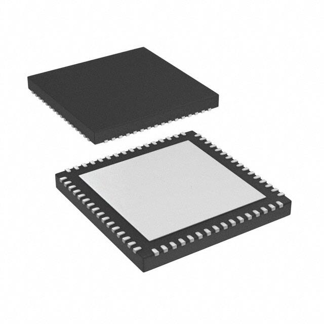


 工商网监
湘ICP备2023018690号
工商网监
湘ICP备2023018690号
