SMD Schottky Barrier Diode
SMD Diodes Specialist
C DBU0230L-HF (RoHS Device)
I o = 200 mA V R = 3 0 Volts Features
H alogen free. Low forward voltage. Designed for mounting on small surface. Extremely thin / leadless package. Majority carrier conduction.
0.039(1.00) 0.031(0.80)
0603(1608)
0.071(1.80) 0.063(1.60)
Mechanical data
0.033(0.85)
C ase: 0603(1608) standard package, molded plastic. Terminals: Gold plated, solderable per MIL-STD-750,method 2026. Marking code: cathode band & BA Mounting position: Any. Weight: 0.003 gram(approx.).
0.027(0.70)
0.014(0.35) Typ.
0.012 (0.30) Typ.
0.028(0.70) Typ.
Dimensions in inches and (millimeter)
Maximum Rating ( at T A =25 C unless otherwise noted)
O
Parameter
Repetitive peak reverse voltage Reverse voltage Average forward current Forward current,surge peak Power Dissipation Storage temperature Junction temperature
Conditions
Symbol Min Typ Max Unit
V RRM VR IO 35 30 200 V V mA
8.3ms single half sine-wave superimposed on rate load(JEDEC method)
I FSM PD T STG Tj -40
1 150 +125 +125
A mW
O
C C
O
Electrical Characteristics ( at T A =25 C unless otherwise noted)
O
Parameter
Forward voltage Reverse current I F = 2 00 mA VR = 10 V
Conditions
Symbol Min Typ Max Unit
VF IR 0.5 30 V uA
REV:A
QW-G1047
Page 1
Comchip Technology CO., LTD.
�SMD Schottky Barrier Diode
SMD Diodes Specialist
RATING AND CHARACTERISTIC CURVES (CDBU0230L-HF)
F ig. 2 - Reverse characteristics
1 000 1m
1 00
R everse current ( A )
Forward current (mA )
100u
75 C
O
10u
25 C
O
10
C
1u
5 12
O
C
C
O
25
1
75
O
-25
O
C
100n
-25 C
O
0 0 0.1 0.2 0.3 0.4 0.5 0.6 0.7 0.8
10n 0 5 10 15 20 25 30
Forward voltage (V)
Reverse voltage (V)
Fig.3 - Capacitance between terminals characteristics
Capacitance between terminals ( P F)
100
Fig.4 - Current derating curve
Average forward current(%)
f = 1 MHz Ta = 25 C
100
80
10
60
40
20
1 0 5 10 15 20 25 30
0 0 25 50 75 100
O
125
150
Reverse voltage (V)
Ambient temperature ( C)
Fig. 5 - VF Dispersion map
450
Ta=25 C IF=200mA n=30pcs
O
Fig. 6 - IR Dispersion map
50 45
Ta=25 C VR=10V n=30pcs
O
Fig. 7 - CT Dispersion map
30 29
Ta=25 C F=1MHz VR=0V n=10pcs
O
35 30 25 20 15 10 5
AVG:4.1816uA
Capacitance between terminals(pF)
Forward voltage (mV)
Reverse current (uA)
440
40
28 27 26 25 24 23 22 21 20
AVG:22.8pF
430
420
410
AVG:421.28mV
400
0
REV:A
QW-G1047
Page 2
Comchip Technology CO., LTD.
�S MD Schottky Barrier Diode
SMD Diodes Specialist
Reel Taping Specification
P0 P1 d Index hole E T
F B
Polarity
W C
P
A
12 0
o
D2
D1 D
W1
Trailer ....... .......
10 pitches (min)
Device ....... ....... ....... .......
Leader ....... .......
10 pitches (min)
End
Start
Direction of Feed
SYMBOL
A
1.00 ± 0.10
0.039 ± 0.004
B
1.85 ± 0.10
0.073 ± 0.004
C
1.00 ± 0.10
0.039 ± 0.004
d
1.55 ± 0.05
0.061 ± 0.002
D
178 ± 1
7.008 ± 0.04
D1
60.0 MIN.
2.362 MIN.
D2
13.0 ± 0.20
0.512 ± 0.008
U/0603
(mm) (inch)
SYMBOL
E
1.75 ± 0.10
0.069 ± 0.004
F
3.50 ± 0.05
0.138 ± 0.002
P
4.00 ± 0.10
0.157 ± 0.004
P0
4.00 ± 0.10
0.157 ± 0.004
P1
2.00 ± 0.05
0.079 ± 0.004
T
0.23 ± 0.05
0.009 ± 0.002
W
8.00 ± 0.20
0.315 ± 0.008
W1
13.5 MAX.
0.531 MAX.
U/0603
(mm) (inch)
REV:A
QW-G1047
Page 3
Comchip Technology CO., LTD.
�SMD Schottky Barrier Diode
SMD Diodes Specialist
Marking Code
Park Number CDBU0230L-HF Marking Code
BA
BA
Suggested PAD Layout
U/0603 SIZE (mm) A B C D E 1.70 0.60 0.80 2.30 1.10 (inch) 0.067 0.024 0.031
C D A E
0.091
B
0.043
Standard Package
Qty per Reel Case Type (Pcs) U/0603 4000 Reel Size (inch) 7
REV:A
QW-G1047
Page 4
Comchip Technology CO., LTD.
�
很抱歉,暂时无法提供与“CDBU0230L-HF”相匹配的价格&库存,您可以联系我们找货
免费人工找货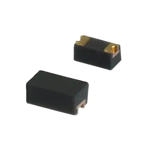


 工商网监
湘ICP备2023018690号
工商网监
湘ICP备2023018690号
