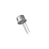
NPN 2N3019 – 2N3020 SILICON PLANAR EPITAXIAL TRANSISTORS
The 2N3019 and 2N3020 are NPN transistors mounted in TO-39 metal case . They are intended for high-current, high-frequency amplifier applications. They feature high gain and low saturation voltages. Compliance to RoHS
ABSOLUTE MAXIMUM RATINGS Symbol
VCEO VCBO VEBO IC PD PD TJ TStg
Collector-Emitter Voltage Collector-Base Voltage Emitter-Base Voltage Collector Current Total Power Dissipation Total Power Dissipation Junction Temperature Storage Temperature range @ Tamb = 25° @ Tcase= 25°
Ratings
2N3019 2N3020 2N3019 2N3020 2N3019 2N3020 2N3019 2N3020 2N3019 2N3020 2N3019 2N3020 2N3019 2N3020 2N3019 2N3020
Value
80 140 7 1 0.8
Unit
V V V A Watts
5 200 -65 to +200 °C °C
THERMAL CHARACTERISTICS Symbol
RthJ-a RthJ-c
Ratings
Thermal Resistance, Junction to ambient in free air Thermal Resistance, Junction to case 2N3019 2N3020 2N3019 2N3020
Value
35 219
Unit
°C/W °C/W
COMSET SEMICONDUCTORS
1/3
�NPN 2N3019 – 2N3020
ELECTRICAL CHARACTERISTICS
TC=25°C unless otherwise noted
Symbol
ICBO IEBO VCEO VCBO VEBO
Ratings
Collector Cutoff Current
Test Condition(s)
VCB =950 V, IE =0 VCB =90 V, IE =0, Tj =150°C
Min Typ Mx Unit
80 140 7 50 30 90 40 100 40 50 30 15 40 100 80 80 30 10 10 10 100 120 300 120 100 0.2 0.5 1.1 400 200 4 12 60 400 MHz dB pF pF ps V nA µA nA V V V
Emitter Cutoff Current
VEB =5 V, IC =0
Collector Emitter Breakdown IC =10 mA, IB =0 Voltage Collector Base Breakdown IC =100 µA, IE =0 Voltage Emitter Base Breakdown IE =100 µA, IC =0 Voltage
IC =0.1 mA, VCE =10 V IC =10 mA, VCE =10 V IC =150 mA, VCE =10 V
hFE (1)
DC Current Gain
IC =500 mA, VCE =10 V IC =1 A, VCE =10 V IC =150 mA, VCE =10 V Tamb = -55°C
2N3019 2N3020 2N3019 2N3020 2N3019 2N3020 2N3019 2N3020 2N3019 2N3020 2N3019 2N3020 2N3019 2N3020 2N3019 2N3020 2N3019 2N3020 2N3019 2N3020 2N3019 2N3020 2N3019 2N3019 2N3020 2N3019 2N3020 2N3019 2N3019 2N3020 2N3019 2N3020 2N3019 2N3019 2N3020 2N3019 2N3020 2N3019 2N3020
-
VCE(SAT) (1) VBE(SAT) (1) fT hfe NF CCBO CEBO rbb’Cb’c
Collector-Emitter saturation Voltage Base-Emitter saturation Voltage Transition frequency Small Signal Current Gain Noise Figure Collector-Base capacitance Emitter-Base capacitance Feedback Time Constant
IC =150 mA, IB =15 mA IC =500 mA, IB =50 mA IC =150 mA, IB =15 mA IC =50 mA, VCE =10 V f = 20 MHz IC =1 mA, VCE =5 V f = 1 kHz IC=-100 µA, VCE =10 V f = 1 kHz, Rg = 1kΩ IE = 0 ,VCB=10 V f = 1 MHz IC = 0 ,VEB=0.5 V f = 1 MHz IC =10 mA, VCE =10 V f = 4 MHz
(1) Pulse conditions : tp < 300 µs, δ =2%
COMSET SEMICONDUCTORS
2/3
�NPN 2N3019 – 2N3020
MECHANICAL DATA CASE TO-39
DIMENSIONS (mm)
min A B D E F G H I L 12.7 5.08 45° typ max 0.49 6.6 8.5 9.4 1.2 0.9 -
Pin 1 : Pin 2 : Case :
Emitter Base Collector
Information furnished is believed to be accurate and reliable. However, CS assumes no responsability for the consequences of use of such information nor for errors that could appear.
Data are subject to change without notice.
COMSET SEMICONDUCTORS
3/3
�
很抱歉,暂时无法提供与“2N3019”相匹配的价格&库存,您可以联系我们找货
免费人工找货