JIANGSU CHANGJING ELECTRONICS TECHNOLOGY CO., LTD
SOT-523 Plastic-Encapsulate MOSFETS
2SK3019
N-channel MOSFET
V(BR)DSS
ID
RDS(on)MAX
SOT-523
8Ω@4V
30 V
100mA
13Ω@2.5V
1. GATE
2. SOURCE
3. DRAIN
FEATURE
Low on-resistance
z
Fast switching speed
z
Low voltage drive makes this device ideal for
Portable equipment
APPLICATION
Interfacing , Switching
z
z
Easily designed drive circuits
Easy to parallel
z
z
Equivalent Circuit
MARKING
MOSFET MAXIMUM RATINGS (Ta = 25°C unless otherwise noted)
Symbol
���Parameter
�������Value
���Unit
�VDS
Drain-Source Voltage
30
V
VGS
Gate-Source Voltage
±20
V
ID
Continuous Drain Current
0.1
A
RθJA
Thermal Resistance, Junction-to-Ambient
833
℃ /W
PD
Power Dissipation
0.15
W
TJ
Junction Temperature
150
℃
Tstg
Storage Temperature
www.jscj-elec.com
-55~+150
1
℃
Rev. - 1.0
�MOSFET ELECTRICAL CHARACTERISTICS
Ta =25 ℃ unless otherwise specified
Parameter
Symbol
Test Condition
Min
Typ
Max
Units
Off Characteristics
Drain-Source Breakdown Voltage
VDS
VGS = 0V, ID = 10µA
Zero Gate Voltage Drain Current
IDSS
VDS =30V,VGS = 0V
Gate –Source leakage current
IGSS
VGS =±20V, VDS = 0V
Gate Threshold Voltage
VGS(th)
VDS = 3V, ID =100µA
Drain-Source On-Resistance
RDS(on)
Forward Transconductance
gFS
30
V
0.8
1
µA
±2
µA
1.5
V
VGS = 4V, ID =10mA
3.8
8
Ω
VGS =2.5V,ID =1mA
6
13
Ω
VDS =3V, ID = 10mA
20
mS
Dynamic Characteristics*
Input Capacitance
Ciss
Output Capacitance
Coss
Reverse Transfer Capacitance
13
pF
9
pF
Crss
4
pF
td(on)
15
ns
VGS =5V, VDD =5V,
35
ns
ID =10mA, Rg=10Ω, RL=500Ω,
80
ns
80
ns
VDS =5V,VGS =0V,f =1MHz
Switching Characteristics*
Turn-On Delay Time
Rise Time
Turn-Off Delay Time
Fall Time
tr
td(off)
tf
* These parameters have no way to verify.
www.jscj-elec.com
2
Rev. - 1.0
�Typical Characteristics
Transfer Characteristics
Output Characteristics
200
Ta=25℃
3.0V
4.0V
Pulsed
200
VDS=3V
Ta=25℃
100
3.5V
Pulsed
ID
120
DRAIN CURRENT
DRAIN CURRENT
ID
(mA)
(mA)
160
2.5V
80
2.0V
40
0
1
2
3
4
DRAIN TO SOURCE VOLTAGE
VDS
10
3
VGS=1.5V
0
30
1
5
0
1
2
3
GATE TO SOURCE VOLTAGE
(V)
RDS(ON) —— ID
RDS(ON) ——
VGS
4
(V)
VGS
15
50
Ta=25℃
Ta=25℃
Pulsed
Pulsed
30
RDS(ON)
10
ON-RESISTANCE
ON-RESISTANCE
RDS(ON)
( Ω)
( Ω)
12
VGS=2.5V
VGS=4V
3
9
6
ID=100mA
3
ID=50mA
1
3
1
30
10
DRAIN CURRENT
ID
100
0
200
0
4
8
12
GATE TO SOURCE VOLTAGE
(mA)
16
VGS
20
(V)
IS —— VSD
200
SOURCE CURRENT
IS (mA)
100
Ta=25℃
Pulsed
30
10
3
1
0.3
0.1
0.2
0.4
0.6
SOURCE TO DRAIN VOLTAGE
www.jscj-elec.com
0.8
1.0
VSD (V)
3
Rev. - 1.0
�627�����3DFNDJH�2XWOLQH�'LPHQVLRQV�
Symbol
A
A1
A2
b1
b2
c
D
E
E1
e
e1
L
L1
�
Dimensions In Millimeters
Min.
Max.
0.700
0.900
0.000
0.100
0.700
0.800
0.150
0.250
0.250
0.350
0.100
0.200
1.500
1.700
0.700
0.900
1.450
1.750
0.500 TYP.
0.900
1.100
0.400 REF.
0.260
0.460
0°
8°
Dimensions In Inches
Min.
Max.
0.028
0.035
0.000
0.004
0.028
0.031
0.006
0.010
0.010
0.014
0.004
0.008
0.059
0.067
0.028
0.035
0.057
0.069
0.020 TYP.
0.035
0.043
0.016 REF.
0.010
0.018
0°
8°
627���� 6XJJHVWHG�3DG�/D\RXW
�
NOTICE
JSCJ reserves the right to make modifications,enhancements,improvements,corrections or other
changes without further notice to any product herein. JSCJ does not assume any liability arising
out of the application or use of any product described herein.
www.jscj-elec.com
4
Rev. - 1.0
�627�����7DSH�DQG�5HHO
www.jscj-elec.com
5
Rev. - 1.0
�
很抱歉,暂时无法提供与“2SK3019”相匹配的价格&库存,您可以联系我们找货
免费人工找货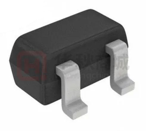


 工商网监
湘ICP备2023018690号
工商网监
湘ICP备2023018690号

