JIANGSU CHANGJIANG ELECTRONICS TECHNOLOGY CO., LTD
SOP8 Plastic-Encapsulate MOSFETS
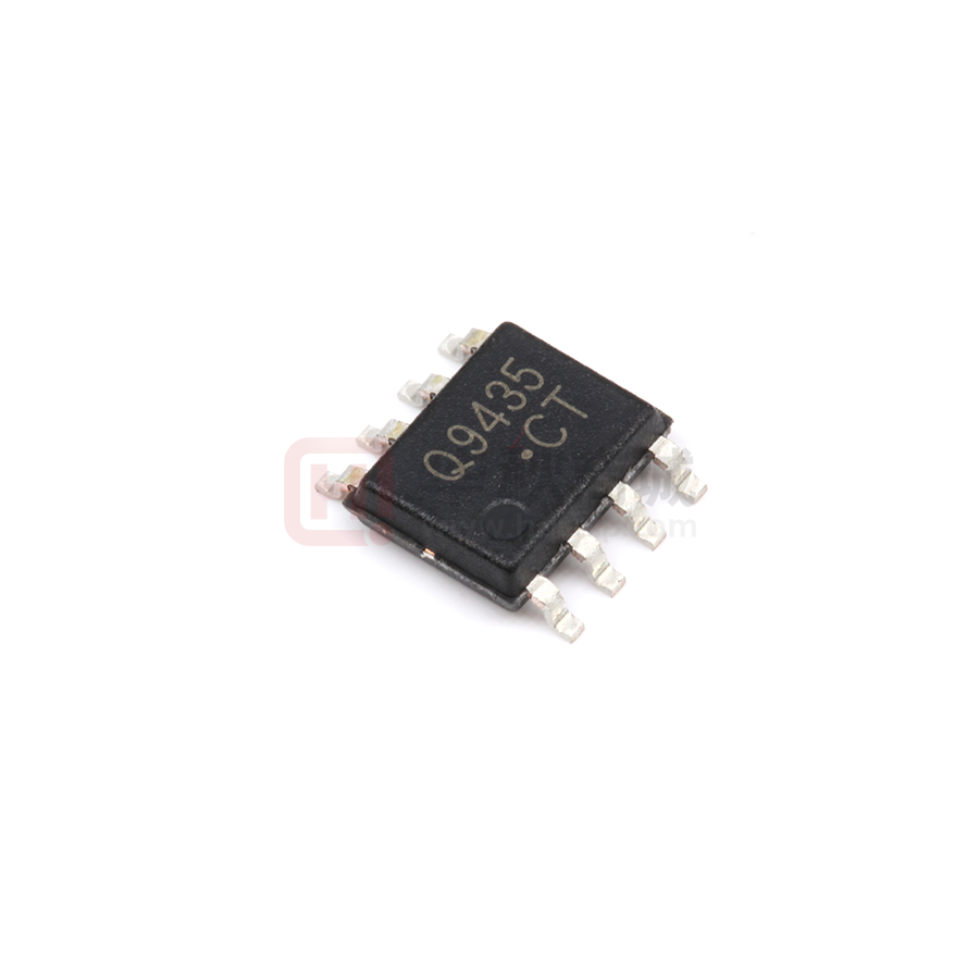
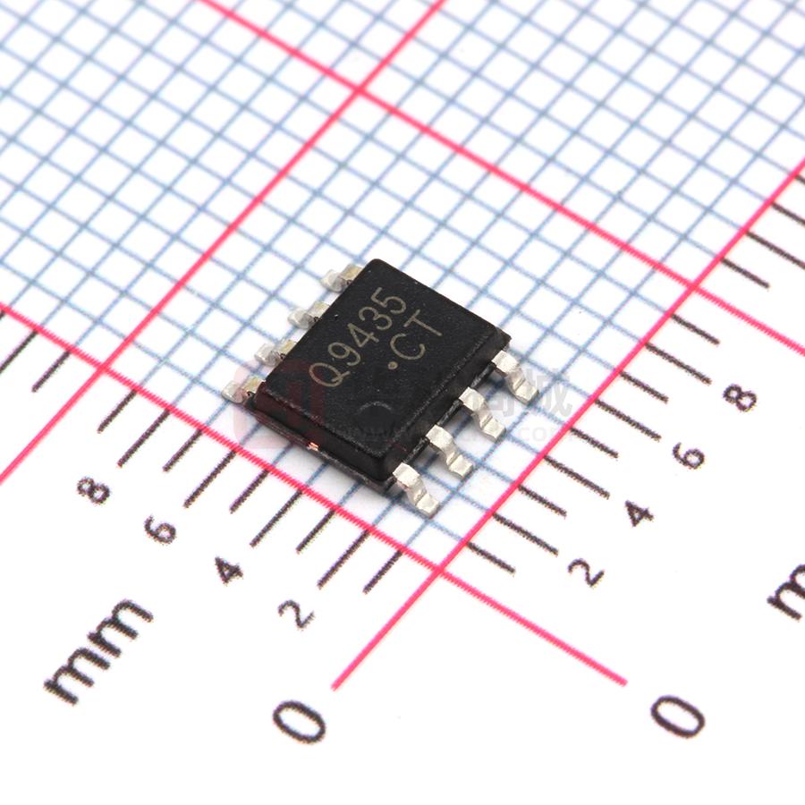
CJQ9435
P-Channel Power MOSFET
V(BR)DSS
ID
RDS(on)MAX
SOP8
60 mΩ@-10V
-30V
70 mΩ@-6V
-5.1A
105 mΩ@-4.5V
DESCRIPTION
The CJQ9435 uses advanced trench technology to provide excellent
RDS(ON), shoot-through immunity, body diode characteristics and ultra-low gate
resistance. This device is ideally suited for use as a low side switch in Notebook
CPU core power conversion.
APPLICATIONS
z
Battery Switch
z
Load Switch
Equivalent Circuit
MARKING:
D
8
D
7
D
6
D
5
Q9435= Device code
YY=Date Code
Solid dot = Pin1 indicator
Solid dot = Green molding compound device,
����if none,the normal device.
1
2
S
3
S
4
S
G
MAXIMUM RATINGS ( Ta=25℃ unless otherwise noted )
Parameter
Symbol
Limit
Unit
Drain-Source Voltage
VDS
-30
V
Gate-Source Voltage
VGS
±20
V
Continuous Drain Current
ID
-5.1
A
Pulsed Drain Current
IDM
-20
A
20
mJ
PD
1.4
W
RθJA
89
℃/W
Junction Temperature
TJ
150
℃
Storage Temperature Range
Tstg
-55 ~+150
℃
Lead Temperature for Soldering Purposes(1/8’’ from case for 10s)
TL
260
℃
Single Pulsed Avalanche Energy
Power Dissipation
Thermal Resistance from Junction to Ambient
EAS
(1)
(1).EAS condition: VDD=-50V,L=0.5mH, RG=25Ω, Starting TJ = 25°C
�����������������������������������������������������������������������������������1����������������������������������������������������������������������
I�Mar����6
���������� �
���
�
�
�
�������
�
Ta =25 Я unless otherwise specified
Parameter
Test Condition
Symbol
Min
Typ
Max
Unit
Off characteristics
Drain-source breakdown voltage
V(BR) DSS
VGS = 0V, ID =-250µA
V
Zero gate voltage drain current
IDSS
VDS =-24V, VGS =0V
-1
µA
Gate-body leakage current
IGSS
VDS =0V, VGS =±20V
±100
nA
VGS(th)
VDS =VGS, ID =-250µA
-1.5
-2.0
V
VGS =-10V, ID =-4.6A
50
60
mΩ
VGS =-6V, ID =-4.1A
60
70
mΩ
VGS =-4.5V, ID =-2A
65
105
mΩ
-30
On characteristics (note1)
Gate-threshold voltage
Static drain-source on-sate resistance
Forward transconductance
RDS(on)
gFS
VDS =-15V, ID =-4.6A
-1.0
5
S
Switching characteristics (note 2)
Total gate charge
Qg
Gate-source charge
Qgs
Gate-drain charge
Qgd
Turn-on delay time
td(on)
Turn-on rise time
Turn-off delay time
tr
td(off)
Turn-off fall time
tf
Gate Resistance
Rg
40
VDS=-15V, VGS=-10V,
ID=-4.6A
nC
4
6.3
30
VDD=-15V,ID=-1A,
60
VGS=-10V,RG=6Ω,
ns
120
RL=15Ω
100
f =1MHz, VDS=0V,
VGS=0V,
5.8
Ω
Drain-Source Diode Characteristics
Drain-source diode forward voltage(note1)
Continuous drain-source diode forward
current
Pulsed drain-source diode forward current
-1.2
V
IS
-5.1
A
ISM
-20
A
VSD
VGS =0V, IS=-2.6A
Notes:
1.
Pulse Test : Pulse Width≤300µs, duty cycle ≤2%.
2.
Guaranteed by design, not subject to production testing.
�
�����������������������������������������������������������������������������������2����������������������������������������������������������������������
I�Mar����6
�7\SLFDO�&KDUDFWHULVWLFV
Output Characteristics
-20
Transfer Characteristics
-5
VGS=-10、-5.0、-4.5、-4.0V
Ta=25℃
Ta=25℃
Pulsed
Pulsed
VGS=-3.5V
-4
-10
-5
ID
VGS=-3.0V
-3
DRAIN CURRENT
DRAIN CURRENT
ID
(A)
(A)
-15
-2
-1
-0
-0
-1
-2
-3
-4
DRAIN TO SOURCE VOLTAGE
RDS(ON)
——
VDS
-0
-5
-0
(V)
-1
-2
GATE TO SOURCE VOLTAGE
-3
VGS
-4
(V)
RDS(ON) —— VGS
ID
100
180
Ta=25℃
Ta=25℃
Pulsed
Pulsed
150
(mΩ)
(mΩ)
80
RDS(ON)
60
ON-RESISTANCE
ON-RESISTANCE
RDS(ON)
VGS=-4.5V
VGS=-10V
40
20
-0
-2
-4
-6
DRAIN CURRENT
IS
——
ID
-8
-10
(A)
120
90
ID=-4.1A
60
30
-2
-4
-6
GATE TO SOURCE VOLTAGE
-8
VGS
-10
(V)
VSD
-10
Ta=25℃
Pulsed
-0.1
SOURCE CURRENT
IS
(A)
-1
-0.01
-1E-3
-1E-4
-1E-5
-0.2
-0.4
-0.6
-0.8
SOURCE TO DRAIN VOLTAGE
-1.0
VSD
-1.2
(V)
�
�����������������������������������������������������������������������������������3����������������������������������������������������������������������
I�Mar����6
�SOP8 Package Outline Dimensions
Symbol
A
A1
A2
b
c
D
e
E
E1
L
θ
Dimensions In Millimeters
Min
1.350
Max
1.750
Dimensions In Inches
Min
0.053
Max
0.069
0.100
0.250
1.350
1.550
0.330
0.510
0.170
0.250
4.800
5.000
1.270(BSC)
0.004
0.010
0.053
0.061
0.013
0.020
0.007
0.010
0.189
0.197
0.050(BSC)
5.800
3.800
0.400
6.200
4.000
1.270
0.228
0.150
0.016
0.244
0.157
0.050
0°
8°
0°
8°
SOP8 Suggested Pad Layout
www.cj-elec.com
4
I,Mar,2016
�SOP8 Tape and Reel
Dimensions are in millimeter
Reel Option
D
D1
D2
G
H
I
W1
W2
13''Dia
Ø330.00
100.00
13.00
R151.00
R56.00
R6.50
12.40
17.60
G.W.(kg)
REEL
4,000 pcs
www.cj-elec.com
Reel Size
Box
13 inch
8,000 pcs
Box Size(mm)
Carton
Carton Size(mm)
360×360×65
64,000 pcs
565×380×390
5
I,Mar,2016
�
很抱歉,暂时无法提供与“CJQ9435”相匹配的价格&库存,您可以联系我们找货
免费人工找货- 国内价格
- 5+0.51626
- 50+0.46961
- 500+0.40741
- 1000+0.36076
- 2500+0.33899


 工商网监
湘ICP备2023018690号
工商网监
湘ICP备2023018690号
