Freescale Semiconductor
Technical Data
Document Number: MRFE6S9125N
Rev. 0, 10/2007
RF Power Field Effect Transistors
N - Channel Enhancement - Mode Lateral MOSFETs
Designed for broadband commercial and industrial applications with frequencies up to 1000 MHz. The high gain and broadband performance of these devices make them ideal for large-signal, common-source amplifier applications
in 28 volt base station equipment.
N - CDMA Application
• Typical Single - Carrier N - CDMA Performance @ 880 MHz, VDD = 28 Volts,
IDQ = 950 mA, Pout = 27 Watts Avg., IS - 95 CDMA (Pilot, Sync, Paging, Traffic
Codes 8 Through 13) Channel Bandwidth = 1.2288 MHz. PAR = 9.8 dB @
0.01% Probability on CCDF.
Power Gain — 20.2 dB
Drain Efficiency — 31%
ACPR @ 750 kHz Offset = - 45.7 dBc in 30 kHz Bandwidth
• Capable of Handling 10:1 VSWR, @ 32 Vdc, 880 MHz, 3 dB Overdrive,
Designed for Enhanced Ruggedness
GSM EDGE Application
• Typical GSM EDGE Performance: VDD = 28 Volts, IDQ = 700 mA,
Pout = 60 Watts Avg., Full Frequency Band (865 - 960 MHz or 920 - 960 MHz)
Power Gain — 20 dB
Drain Efficiency — 40%
Spectral Regrowth @ 400 kHz Offset = - 63 dBc
Spectral Regrowth @ 600 kHz Offset = - 78 dBc
EVM — 1.8% rms
GSM Application
• Typical GSM Performance: VDD = 28 Volts, IDQ = 700 mA, Pout =
125 Watts, Full Frequency Band (920 - 960 MHz)
Power Gain — 19 dB
Drain Efficiency — 62%
Features
• Characterized with Series Equivalent Large - Signal Impedance Parameters
• Internally Matched for Ease of Use
• Integrated ESD Protection
• 225°C Capable Plastic Package
• RoHS Compliant
• In Tape and Reel. R1 Suffix = 500 Units per 44 mm, 13 inch Reel.
MRFE6S9125NR1
MRFE6S9125NBR1
880 MHz, 27 W AVG., 28 V
SINGLE N - CDMA, GSM EDGE
LATERAL N - CHANNEL
RF POWER MOSFETs
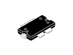
CASE 1486 - 03, STYLE 1
TO - 270 WB - 4
PLASTIC
MRF6S9125NR1
CASE 1484 - 04, STYLE 1
TO - 272 WB - 4
PLASTIC
MRF6S9125NBR1
Table 1. Maximum Ratings
Rating
Symbol
Value
Unit
Drain - Source Voltage
VDSS
- 0.5, +66
Vdc
Gate - Source Voltage
VGS
- 0.5, +12
Vdc
Maximum Operation Voltage
VDD
32, +0
Vdc
Storage Temperature Range
Tstg
- 65 to +150
°C
Case Operating Temperature
TC
150
°C
Operating Junction Temperature (1,2)
TJ
225
°C
Symbol
Value (2,3)
Unit
Table 2. Thermal Characteristics
Characteristic
Thermal Resistance, Junction to Case
Case Temperature 80°C, 125 W CW
Case Temperature 76°C, 27 W CW
RθJC
0.44
0.45
°C/W
1. Continuous use at maximum temperature will affect MTTF.
2. MTTF calculator available at http://www.freescale.com/rf. Select Tools (Software & Tools)/Calculators to access MTTF calculators
by product.
3. Refer to AN1955, Thermal Measurement Methodology of RF Power Amplifiers. Go to http://www.freescale.com/rf.
Select Documentation/Application Notes - AN1955.
© Freescale Semiconductor, Inc., 2007. All rights reserved.
RF Device Data
Freescale Semiconductor
MRFE6S9125NR1 MRFE6S9125NBR1
1
�Table 3. ESD Protection Characteristics
Test Methodology
Class
Human Body Model (per JESD22 - A114)
1B (Minimum)
Machine Model (per EIA/JESD22 - A115)
A (Minimum)
Charge Device Model (per JESD22 - C101)
IV (Minimum)
Table 4. Moisture Sensitivity Level
Test Methodology
Per JESD 22 - A113, IPC/JEDEC J - STD - 020
Rating
Package Peak Temperature
Unit
3
260
°C
Table 5. Electrical Characteristics (TC = 25°C unless otherwise noted)
Characteristic
Symbol
Min
Typ
Max
Unit
Zero Gate Voltage Drain Leakage Current
(VDS = 66 Vdc, VGS = 0 Vdc)
IDSS
—
—
10
μAdc
Zero Gate Voltage Drain Leakage Current
(VDS = 28 Vdc, VGS = 0 Vdc)
IDSS
—
—
1
μAdc
Gate - Source Leakage Current
(VGS = 5 Vdc, VDS = 0 Vdc)
IGSS
—
—
10
μAdc
Gate Threshold Voltage
(VDS = 10 Vdc, ID = 400 μAdc)
VGS(th)
1
2.1
3
Vdc
Gate Quiescent Voltage
(VDD = 28 Vdc, ID = 950 mAdc, Measured in Functional Test)
VGS(Q)
2
2.86
4
Vdc
Drain - Source On - Voltage
(VGS = 10 Vdc, ID = 2.74 Adc)
VDS(on)
0.05
0.24
0.3
Vdc
Reverse Transfer Capacitance
(VDS = 28 Vdc ± 30 mV(rms)ac @ 1 MHz, VGS = 0 Vdc)
Crss
—
1.9
—
pF
Output Capacitance
(VDS = 28 Vdc ± 30 mV(rms)ac @ 1 MHz, VGS = 0 Vdc)
Coss
—
64
—
pF
Input Capacitance
(VDS = 28 Vdc, VGS = 0 Vdc ± 30 mV(rms)ac @ 1 MHz)
Ciss
—
350
—
pF
Off Characteristics
On Characteristics
Dynamic Characteristics (1)
Functional Tests (In Freescale Test Fixture, 50 ohm system) VDD = 28 Vdc, IDQ = 950 mA, Pout = 27 W Avg. N - CDMA, f = 880 MHz,
Single - Carrier N - CDMA, 1.2288 MHz Channel Bandwidth Carrier. ACPR measured in 30 kHz Channel Bandwidth @ ±750 kHz Offset.
PAR = 9.8 dB @ 0.01% Probability on CCDF.
Power Gain
Gps
19
20.2
24
dB
Drain Efficiency
ηD
29
31
—
%
ACPR
—
- 45.7
- 44
dBc
IRL
—
- 18
-9
dB
Adjacent Channel Power Ratio
Input Return Loss
1. Part is internally input matched.
(continued)
MRFE6S9125NR1 MRFE6S9125NBR1
2
RF Device Data
Freescale Semiconductor
�Table 5. Electrical Characteristics (TC = 25°C unless otherwise noted) (continued)
Characteristic
Symbol
Min
Typ
Max
Unit
Typical GSM EDGE Performances (In Freescale GSM EDGE Test Fixture, 50 ohm system) VDD = 28 Vdc, IDQ = 700 mA,
Pout = 60 W Avg., 920 - 960 MHz, EDGE Modulation
Power Gain
Gps
—
20
—
dB
Drain Efficiency
ηD
—
40
—
%
Error Vector Magnitude
EVM
—
1.8
—
% rms
Spectral Regrowth at 400 kHz Offset
SR1
—
- 63
—
dBc
Spectral Regrowth at 600 kHz Offset
SR2
—
- 78
—
dBc
Typical CW Performances (In Freescale GSM Test Fixture, 50 ohm system) VDD = 28 Vdc, IDQ = 700 mA, Pout = 125 W, 920 - 960 MHz
Power Gain
Gps
—
19
—
dB
Drain Efficiency
ηD
—
62
—
%
Input Return Loss
IRL
—
- 12
—
dB
P1dB
—
125
—
W
Pout @ 1 dB Compression Point, CW
(f = 880 MHz)
Typical Performances (In Freescale Test Fixture, 50 ohm system) VDD = 28 Vdc, IDQ = 950 mA, 865 - 900 MHz Bandwidth
VBW
Video Bandwidth @ 125 W PEP Pout where IM3 = - 30 dBc
(Tone Spacing from 100 kHz to VBW)
—
10
—
ΔIMD3 = IMD3 @ VBW frequency - IMD3 @ 100 kHz


 工商网监
湘ICP备2023018690号
工商网监
湘ICP备2023018690号
