ON Semiconductor
Is Now
To learn more about onsemi™, please visit our website at
www.onsemi.com
onsemi and and other names, marks, and brands are registered and/or common law trademarks of Semiconductor Components Industries, LLC dba “onsemi” or its affiliates and/or
subsidiaries in the United States and/or other countries. onsemi owns the rights to a number of patents, trademarks, copyrights, trade secrets, and other intellectual property. A listing of onsemi
product/patent coverage may be accessed at www.onsemi.com/site/pdf/Patent-Marking.pdf. onsemi reserves the right to make changes at any time to any products or information herein, without
notice. The information herein is provided “as-is” and onsemi makes no warranty, representation or guarantee regarding the accuracy of the information, product features, availability, functionality,
or suitability of its products for any particular purpose, nor does onsemi assume any liability arising out of the application or use of any product or circuit, and specifically disclaims any and all
liability, including without limitation special, consequential or incidental damages. Buyer is responsible for its products and applications using onsemi products, including compliance with all laws,
regulations and safety requirements or standards, regardless of any support or applications information provided by onsemi. “Typical” parameters which may be provided in onsemi data sheets and/
or specifications can and do vary in different applications and actual performance may vary over time. All operating parameters, including “Typicals” must be validated for each customer application
by customer’s technical experts. onsemi does not convey any license under any of its intellectual property rights nor the rights of others. onsemi products are not designed, intended, or authorized
for use as a critical component in life support systems or any FDA Class 3 medical devices or medical devices with a same or similar classification in a foreign jurisdiction or any devices intended for
implantation in the human body. Should Buyer purchase or use onsemi products for any such unintended or unauthorized application, Buyer shall indemnify and hold onsemi and its officers, employees,
subsidiaries, affiliates, and distributors harmless against all claims, costs, damages, and expenses, and reasonable attorney fees arising out of, directly or indirectly, any claim of personal injury or death
associated with such unintended or unauthorized use, even if such claim alleges that onsemi was negligent regarding the design or manufacture of the part. onsemi is an Equal Opportunity/Affirmative
Action Employer. This literature is subject to all applicable copyright laws and is not for resale in any manner. Other names and brands may be claimed as the property of others.
�ADP3611
Dual Bootstrapped, High
Voltage MOSFET Driver
with Output Disable
The ADP3611 is a dual MOSFET driver optimized for driving two
N−channel switching MOSFETs in nonisolated synchronous buck
power converters used to power CPUs in portable computers. The
driver impedances have been chosen to provide optimum
performance in multiphase regulators at up to 25 A per phase. The
high−side driver can be bootstrapped relative to the switch node of
the buck converter and is designed to accommodate the high voltage
slew rate associated with floating high−side gate drivers. An internal
synchronous MOSFET is used to replace an external bootstrap
Schottky diode. This allows a larger high side gate voltage for
increased efficiency.
The ADP3611 includes an anticross−conduction protection circuit,
undervoltage lockout to hold the switches off until the driver has
sufficient voltage for proper operation, a crowbar input that turns on
the low−side MOSFET independently of the input signal state, and a
low−side MOSFET disable pin to provide higher efficiency at light
loads. The SD pin shuts off both the high−side and the low−side
MOSFETs to prevent rapid output capacitor discharge during system
shutdown.
The ADP3611 is specified over the extended commercial
temperature range of −10°C to 100°C and is available in a 10−lead
MSOP package and 8−lead DFN 2x2 mm package.
All−in−one Synchronous Buck Driver
One PWM Signal Generates Both Drives
Anticross−conduction Protection Circuitry
Output Disable Function
Crowbar Control
Synchronous Override Control
This is a Pb−Free Device
October, 2008 − Rev. 0
MARKING DIAGRAMS
XXMG
G
X = Specific Device Code
M = Date Code
G = Pb−Free Package
(Note: Microdot may be in either location)
Mobile Computing CPU Core Power Converters
Multiphase Desk−note CPU Supplies
Single−supply Synchronous Buck Converters
Nonsynchronous−to−Synchronous Drive Conversion
© Semiconductor Components Industries, LLC, 2008
MSOP10
JRM SUFFIX
CASE 846AC
XX MG
G
Applications
•
•
•
•
1
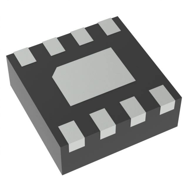
DFN8
CP SUFFIX
CASE 506AA
1
Features
•
•
•
•
•
•
•
http://onsemi.com
ORDERING INFORMATION
See detailed ordering and shipping information in the package
dimensions section on page 2 of this data sheet.
1
Publication Order Number:
ADP3611/D
�ADP3611
SIMPLIFIED FUNCTIONAL BLOCK DIAGRAM
Figure 1. MSOP−10 Package Block Diagram
GENERAL APPLICATION CIRCUIT
Figure 2. MSOP−10 Package Application Circuit
Table 1. ORDERING INFORMATION
Temperature
Range
Package Description
Package
Option
Quantity
per Reel†
Branding
ADP3611JRMZ−REEL*
−10°C to 100°C
10−Lead Mini Small Outline Package (MSOP)
RM−10
3000
3611
ADP3611MNR2G*
−10°C to 100°C
8−Lead 2x2 mm Package
DFN
3000
D6 M
Model
* Z or G = Pb−Free Part
†For information on tape and reel specifications, including part orientation and tape sizes, please refer to our Tape and Reel Packaging Specification
Brochure, BRD8011/D.
http://onsemi.com
2
�ADP3611
Table 2. ELECTRICAL CHARACTERISTICS (VCC = SD = 5 V, BST − SW = 5 V, TA = −10°C to 100°C, unless otherwise noted)
Parameter
Symbol
Conditions
Min
Typ
Max
Unit
LOGIC INPUTS (IN, SD, DRVLSD, CROWBAR)
Input Voltage High
VIH
Input Voltage Low
VIL
2.0
V
0.8
Input Current
IIN
Inputs = 0 V or 5 V, IN, SD, DRVLSD
CROWBAR Resistance
RIN
Resistance from CROWBAR to GND
250
kW
CLOAD = 3 nF, Figure 3
20
ns
DRVLSD Propagation Delay Time
tpdlDRVLSD
tpdhDRVLSD
−1
+1
V
mA
HIGH−SIDE DRIVER
Output Resistance, Sourcing Current
1.9
3.3
W
Output Resistance, Sinking Current
1.0
2.3
W
Transition Times
trDRVH
CLOAD = 3 nF, Figure 4
20
35
ns
tfDRVH
CLOAD = 3 nF, Figure 4
15
25
ns
tpdhDRVH
CLOAD = 3 nF, Figure 4
30
60
ns
tpdlDRVH
CLOAD = 3 nF, Figure 4
20
40
ns
Output Resistance, Sourcing Current
1.7
3.3
W
Output Resistance, Sinking Current
0.8
2.3
W
Propagation Delay Times (Note 1)
15
LOW−SIDE DRIVER
Transition Times
Propagation Delay Times
(Notes 1 and 2)
SW Transition Timeout (Note 2)
Zero−crossing Threshold
trDRVL
CLOAD = 3 nF, Figure 4
20
30
ns
tfDRVL
CLOAD = 3 nF, Figure 4
15
25
ns
tpdhDRVL
CLOAD = 3 nF, Figure 4
15
40
ns
tpdlDRVL
CLOAD = 3 nF, Figure 4
15
30
ns
270
450
ns
tSWTO
SW = 2 V
150
VZC
1.8
RBOOT
10
V
BOOTSTRAP RECTIFIER
Output Resistance
18
W
SWITCH NODE RESISTOR
Switch Node Resistor
RSW
EN = 0 V
3
kW
SUPPLY
Supply Voltage Range
VCC
4.6
5.5
V
Supply Current − Normal Mode
ISYS(NM)
ICC + IBST, IN = 0 V or 5 V
0.5
1
mA
Supply Current − Shutdown Mode
ISYS(SD)
ICC + IBST, SD = 0 V
30
200
mA
4.5
Undervoltage Lockout Threshold
VCC Rising
4
4.35
Undervoltage Lockout Hysteresis
(Note 3)
VCC Falling
50
210
V
mV
NOTE: All limits at temperature extremes are guaranteed via correlation using standard statistical quality control (SQC) methods.
1. For propagation delays, tpdh refers to the specified signal going high, and tpdl refers to the signal going low with transitions measured at 50%.
2. The turn−on of DRVL is initiated after IN goes low by either SW crossing a ~1 V threshold or by expiration of tSWTO.
3. Guaranteed by characterization, not production tested.
http://onsemi.com
3
�ADP3611
IN
2.0 V
DRVLSD
0.8 V
tpdlDRVLSD
tpdhDRVLSD
DRVL
Figure 3. Output Disable Timing Diagram (Timing is Referenced to
the 90% and 10% Points Unless Otherwise Noted)
IN
tpdlDRVL tfDRVL
trDRVL
tpdlDRVH
DRVL
tpdhDRVH
DRVH−SW
tfDRVH
trDRVH
VTH
VTH
SW
1V
tpdhDRVL
≤ tSWTO
Figure 4. Nonoverlap Timing Diagram (Timing is Referenced to the
90% and 10% Points Unless Otherwise Noted)
http://onsemi.com
4
�ADP3611
Table 3. ABSOLUTE MAXIMUM RATINGS (Unless otherwise specified, all voltages are referenced to GND.)
Parameter
VCC
BST, DRVH
DC
t < 200 ns
BST to SW
Rating
Unit
−0.3 to +6
V
−0.3 to +26
−0.3 to +31
V
−0.3 to +6
V
BST to VCC
DC
t < 200 ns
−0.3 to +21
−0.3 to +26
V
SW
DC
t < 200 ns
−1 to +21
−6 to +26
V
−0.3 to +6
V
SW − 0.3 to BST + 0.3
V
−0.3 to +6
−5 to +6
V
−0.3 to +6
V
340
220
°C/W
143
°C/W
Operating Ambient Temperature Range
−10 to +100
°C
Junction Temperature Range
−10 to +150
°C
Storage Temperature Range
−65 to +150
°C
300
215
220
°C
DRVH to SW
DRVH
DRVL
DC
t < 200 ns
All Other Inputs and Outputs
qJA MSOP−10 Package
2−Layer Board
4−Layer Board
qJA QFN−8 2 mm x 2 mm Package
Lead Temperature Range
Soldering (10 s)
Vapor Phase (60 s)
Infrared (15 s)
Stresses exceeding Maximum Ratings may damage the device. Maximum Ratings are stress ratings only. Functional operation above the
Recommended Operating Conditions is not implied. Extended exposure to stresses above the Recommended Operating Conditions may affect
device reliability.
NOTE: This device is ESD sensitive. Use standard ESD precautions when handling.
Pin Configuration
IN 1
10
BST
SD 2
9
DRVH
8
SW
7
GND
6
DRVL
DRVLSD 3
CROWBAR
4
ADP3611
TOP VIEW
(Not to Scale)
VCC 5
Figure 5. 10−Lead MSOP Package
BST
IN
SD
DRVLSD
VCC
ADP3611
TOP VIEW
(Not to Scale)
DRVH
SW
DRVL
Figure 6. 8−Lead DFN 2 x 2 mm Package
http://onsemi.com
5
�ADP3611
Table 4. PIN FUNCTION DESCRIPTIONS
Pin No.
QFN
Pin No.
MSOP
Symbol
1
1
IN
Logic Level PWM Input. This pin has primary control of the drive outputs. In normal operation, pulling
this pin low turns on the low−side driver; pulling it high turns on the high−side driver.
2
2
SD
Shutdown Input. When low, this pin disables normal operation, forcing DRVH and DRVL low.
3
3
DRVLSD
4
CROWBAR
4
5
VCC
Input Supply. This pin should be bypassed to GND with a 4.7 mF or larger ceramic capacitor.
5
6
DRVL
Synchronous Rectifier Drive. Output drive for the lower (synchronous rectifier) MOSFET.
Tab
7
GND
Ground. This pin should be closely connected to the source of the lower MOSFET.
6
8
SW
7
9
DRVH
8
10
BST
ÁÁÁÁÁÁÁ
ÁÁÁÁÁ
ÁÁÁÁÁÁÁÁÁÁÁÁÁÁÁÁÁÁÁÁÁÁÁÁ
ÁÁÁÁ
ÁÁÁ
ÁÁÁÁÁ
ÁÁÁÁÁÁÁÁÁÁÁÁÁÁÁÁÁÁÁÁÁÁÁÁ
ÁÁÁÁ
ÁÁÁ
ÁÁÁÁÁ
ÁÁÁÁÁÁÁÁÁÁÁÁÁÁÁÁÁÁÁÁÁÁÁÁ
ÁÁÁÁ
ÁÁÁ
ÁÁÁÁÁ
ÁÁÁÁÁÁÁÁÁÁÁÁÁÁÁÁÁÁÁÁÁÁÁÁ
ÁÁÁÁ
ÁÁÁ
ÁÁÁÁÁ
ÁÁÁÁÁÁÁÁÁÁÁÁÁÁÁÁÁÁÁÁÁÁÁÁ
ÁÁÁÁÁÁÁ
ÁÁÁÁÁ
ÁÁÁÁÁÁÁÁÁÁÁÁÁÁÁÁÁÁÁÁÁÁÁÁ
ÁÁÁÁÁÁÁ
ÁÁÁÁÁ
ÁÁÁÁÁÁÁÁÁÁÁÁÁÁÁÁÁÁÁÁÁÁÁÁ
ÁÁÁÁ
ÁÁÁ
ÁÁÁÁÁ
ÁÁÁÁÁÁÁÁÁÁÁÁÁÁÁÁÁÁÁÁÁÁÁÁ
ÁÁÁÁ
ÁÁÁ
ÁÁÁÁÁ
ÁÁÁÁÁÁÁÁÁÁÁÁÁÁÁÁÁÁÁÁÁÁÁÁ
ÁÁÁÁ
ÁÁÁ
ÁÁÁÁÁ
ÁÁÁÁÁÁÁÁÁÁÁÁÁÁÁÁÁÁÁÁÁÁÁÁ
ÁÁÁÁ
ÁÁÁ
ÁÁÁÁÁ
ÁÁÁÁÁÁÁÁÁÁÁÁÁÁÁÁÁÁÁÁÁÁÁÁ
ÁÁÁÁ
ÁÁÁÁÁ
ÁÁÁÁÁÁÁÁÁÁÁÁÁÁÁÁÁÁÁÁÁÁÁÁ
ÁÁÁÁÁÁÁ
ÁÁÁ
ÁÁÁÁÁ
ÁÁÁÁÁÁÁÁÁÁÁÁÁÁÁÁÁÁÁÁÁÁÁÁ
ÁÁÁÁÁÁÁ
ÁÁÁÁÁ
ÁÁÁÁÁÁÁÁÁÁÁÁÁÁÁÁÁÁÁÁÁÁÁÁ
Description
Synchronous Rectifier Shutdown Input. When low, DRVL is forced low; when high, DRVL is enabled
and controlled by IN and by the adaptive overlap protection control circuitry.
Crowbar Input. When high, DRVL is forced high regardless of the high−side MOSFET switch condition.
Switch Node Input. This pin is connected to the buck−switching node, close to the upper MOSFET’s
source. It is the floating return for the upper MOSFET drive signal. It is also used to monitor the
switched voltage to prevent turn−on of the lower MOSFET until the voltage is below ~1 V.
Buck Drive. Output drive for the upper (buck) MOSFET.
Upper MOSFET Floating Bootstrap Supply. A capacitor connected between the BST and SW pins
holds this bootstrapped voltage for the high−side MOSFET as it is switched.
http://onsemi.com
6
�ADP3611
TYPICAL PERFORMANCE CHARACTERISTICS
Figure 7. DRVH Rise and DRVL Fall Times
CH1 = IN, CH2 = DRVH, CH3 = DRVL
Figure 8. DRVH Fall and DRVL Rise Times
CH1 = IN, CH2 = DRVH, CH3 = DRVL
25
30
VCC = 5 V
C Load = 3 nF
25
VCC = 5 V
C Load = 3 nF
Rise Time
Rise Time
20
15
TIME (ns)
TIME (ns)
20
Fall Time
15
Fall Time
10
10
5
5
0
−10
0
25
50
75
0
−10
100
50
75
100
JUNCTION TEMPERATURE (°C)
Figure 9. DRVH Rise and Fall Times vs.
Temperature
Figure 10. DRVL Rise and Fall Times vs.
Temperature
30
VCC = 5 V
TA = 25°C
50
40
30
20
DRVH
10
20
DRVL
15
10
5
DRVL
1
DRVH
VCC = 5 V
TA = 25°C
25
FALL TIME (ns)
RISE TIME (ns)
25
JUNCTION TEMPERATURE (°C)
60
0
0
2
3
4
6
0
10
1
2
3
4
6
LOAD CAPACITANCE (nF)
LOAD CAPACITANCE (nF)
Figure 11. DRVH and DRVL Rise Times vs.
Load Capacitance
Figure 12. DRVH and DRVL Fall Times vs.
Load Capacitance
http://onsemi.com
7
10
�ADP3611
TYPICAL PERFORMANCE CHARACTERISTICS
50
50
VCC = 5 V
C Load = 3 nF
40
tpdhDRVH
30
TIME (ns)
TIME (ns)
40
tpdhDRVL
20
10
0
25
50
75
20
tpdlDRVL
0
−10
100
0
25
50
75
JUNCTION TEMPERATURE (°C)
JUNCTION TEMPERATURE (°C)
Figure 13. DRVH and DRVL tpdh vs.
Temperature
Figure 14. DRVH and DRVL tpdl vs.
Temperature
100
100
50
VCC = 5 V
C Load = 3 nF
TA = 25°C
VCC = BST = 5 V
C Load = 3 nF
TA = 25°C
40
ISYS CURRENT (mA)
80
60
40
20
30
20
10
0
1
2
3
4
0
5
0
200
400
600
800
1000
INPUT VOLTAGE (V)
IN FREQUENCY (kHz)
Figure 15. IN Pin Input Current vs.
Input Voltage
Figure 16. Supply Current vs. Frequency
0.6
0.5
ISYS CURRENT (mA)
PEAK INPUT CURRENT (mA)
tpdlDRVH
30
10
0
−10
0
VCC = 5 V
C Load = 3 nF
0.4
0.3
0.2
0.1
0
−10
VCC = 5 V
C Load = 3 nF
0
25
50
75
JUNCTION TEMPERATURE (°C)
Figure 17. Supply Current vs. Temperature
http://onsemi.com
8
100
1200
�ADP3611
THEORY OF OPERATION
High−Side Driver
The ADP3611 is a dual MOSFET driver optimized for
driving two N-channel MOSFETs in a synchronous buck
converter topology. A single PWM input signal is all that
is required to properly drive the high-side and the low-side
MOSFETs. Each driver is capable of driving a 3 nF load at
speeds up to 1 MHz. A more detailed description of the
ADP3611 and its features follows. Refer to the detailed
block diagram in Figure 18.
The high-side driver is designed to drive a floating low
RDS(ON) N-channel MOSFET. The bias voltage for the
high-side driver is developed by an external bootstrap
supply circuit, which is connected between the BST and
SW pins.
The bootstrap circuit comprises a diode, D1, and
bootstrap capacitor, CBST. When the ADP3611 is starting
up, the SW pin is at ground, so the bootstrap capacitor
charges up to VCC through D1. Once the supply voltage
ramps up and exceeds the UVLO threshold, the driver is
enabled. When IN goes high, the high-side driver begins to
turn on the high-side MOSFET (Q1) by transferring charge
from CBST. As Q1 turns on, the SW pin rises up to VDCIN,
forcing the BST pin to VDCIN + VC(BST), which is enough
gate-to-source voltage to hold Q1 on. To complete the
cycle, Q1 is switched off by pulling the gate down to the
voltage at the SW pin. When the low-side MOSFET (Q2)
turns on, the SW pin is pulled to ground. This allows the
bootstrap capacitor to charge up to VCC again.
When the driver is enabled, the driver’s output is in phase
with the IN pin. Table 5 shows the relationship between
DRVH and the different control inputs of the ADP3611.
Overlap Protection Circuit
The overlap protection circuit prevents both main power
switches, Q1 and Q2, from being on at the same time. This
is done to prevent shoot-through currents from flowing
through both power switches and the associated losses that
can occur during their on-off transitions. The overlap
protection circuit accomplishes this by adaptively
controlling the delay from Q1’s turn-off to Q2’s turn-on,
and the delay from Q2’s turn-off to Q1’s turn-on.
To prevent the overlap of the gate drives during Q1’s
turn-off and Q2’s turn-on, the overlap circuit monitors the
voltage at the SW pin and DRVH pin. When IN goes low,
Q1 begins to turn off. The overlap protection circuit waits
for the voltage at the SW and DRVH pins to both fall below
1.6 V. Once both of these conditions are met, Q2 begins to
turn on. Using this method, the overlap protection circuit
ensures that Q1 is off before Q2 turns on, regardless of
variations in temperature, supply voltage, gate charge, and
drive current. There is, however, a timeout circuit that
overrides the waiting period for the SW and DRVH pins to
reach 1.6 V. After the timeout period has expired, DRVL is
asserted high regardless of the SW and DRVH voltages. In
the opposite case, when IN goes high, Q2 begins to turn off
after a propagation delay. The overlap protection circuit
waits for the voltage at DRVL to fall below 1.6 V, after
which DRVH is asserted high and Q1 turns on.
Figure 18. Detailed Block Diagram of the ADP3611
Undervoltage Lockout
The undervoltage lockout (UVLO) circuit holds both
MOSFET driver outputs low during VCC supply ramp-up.
The UVLO logic becomes active and in control of the
driver outputs at a supply voltage of no greater than 1.5 V.
The UVLO circuit waits until the VCC supply has reached
a voltage high enough to bias logic level MOSFETs fully
on before releasing control of the drivers to the control pins.
Driver Control Input
The driver control input (IN) is connected to the duty
ratio modulation signal of a switch-mode controller. IN can
be driven by 2.5 V to 5.0 V logic. The output MOSFETs are
driven so that the SW node follows the polarity of IN.
Low−Side Driver
The low-side driver is designed to drive a groundreferenced low RDS(ON) N-channel synchronous rectifier
MOSFET. The bias to the low-side driver is internally
connected to the VCC supply and GND. Once the supply
voltage ramps up and exceeds the UVLO threshold, the
driver is enabled. When the driver is enabled, the driver’s
output is 180° out of phase with the IN pin. Table 5 shows
the relationship between DRVL and the different control
inputs of the ADP3611.
Low−Side Driver Shutdown
The low-side driver shutdown DRVLSD allows a control
signal to shut down the synchronous rectifier. Under light
load conditions, DRVLSD should be pulled low before the
http://onsemi.com
9
�ADP3611
Crowbar Function
polarity reversal of the inductor current to maximize light
load conversion efficiency. DRVLSD can also be pulled
low for reverse voltage protection purposes.
When DRVLSD is low, the low-side driver stays low.
When DRVLSD is high, the low-side driver is enabled and
controlled by the driver signals, as previously described.
In addition to the internal low-side drive time-out circuit,
the ADP3611 includes a CROWBAR input pin to provide
a means for additional overvoltage protection. When
CROWBAR goes high, the ADP3611 turns off DRVH and
turns on DRVL. The crowbar logic overrides the overlap
protection circuit, the shutdown logic, the DRVLSD logic,
and the UVLO protection on DRVL. Thus, the crowbar
function maximizes the overvoltage protection coverage in
the application. The CROWBAR can be either driven by
the CLAMP pin of buck controllers, such as the
ADP3207A, or ADP3210, or controlled by an independent
overvoltage monitoring circuit.
Low−Side Driver Timeout
In normal operation, the DRVH signal tracks the IN
signal and turns off the Q1 high-side switch with a few 10
ns delay (tpdlDRVH) following the falling edge of the input
signal. When Q1 is turned off, DRVL is allowed to go high,
Q2 turns on, and the SW node voltage collapses to zero. But
in a fault condition such as a high-side Q1 switch
drain-source short circuit, the SW node cannot fall to zero,
even when DRVH goes low. The ADP3611 has a timer
circuit to address this scenario. Every time the IN goes low,
a DRVL on-time delay timer is triggered. If the SW node
voltage does not trigger a low-side turn-on, the DRVL
on-time delay circuit does it instead, when it times out with
tSW(TO) delay. If Q1 is still turned on, that is, its drain is
shorted to the source, Q2 turns on and creates a direct short
circuit across the VDCIN voltage rail. The crowbar action
causes the fuse in the VDCIN current path to open. The
opening of the fuse saves the load (CPU) from potential
damage that the high-side switch short circuit could have
caused.
Table 5. ADP3611 Truth Table
CROWBAR
UVLO
SD
DRVLSD
IN
DRVH
DRVL
L
L
H
H
H
H
L
L
L
H
H
L
L
H
L
L
H
L
H
H
L
L
L
H
L
L
L
L
L
L
L
*
*
L
L
L
H
*
*
*
L
L
H
L
*
*
*
L
H
H
H
*
*
*
L
H
* = Don’t Care
APPLICATION INFORMATION
Supply Capacitor Selection
where:
QHSGATE is the total gate charge of the high-side MOSFET.
DVBST is the voltage droop allowed on the high-side
MOSFET drive.
For example, two NTMFS4821N MOSFETs in parallel
have a total gate charge of about 20 nC. For an allowed
droop of 100 mV, the required bootstrap capacitance is
200 nF. A good quality ceramic capacitor should be used,
and derating for the significant capacitance drop of MLCs
at high temperature must be applied. In this example,
selection of 470 nF or even 1 mF would be recommended.
Normally a Schottky diode is recommended for the
bootstrap diode due to its low forward drop, which
maximizes the drive available for the high-side MOSFET.
Using a synchronous MOSFET rectifier instead of a
Schottky diode has the advantage of an even lower forward
voltage drop. A lower forward voltage drop gives a larger
drive voltage for the high-side MOSFET and a lower
conduction loss for the high-side MOSFET. The bootstrap
diode must also be able to handle at least 5 V more than the
maximum battery voltage. The average forward current
can be estimated by
For the supply input (VCC) of the ADP3611, a local
bypass capacitor is recommended to reduce the noise and
to supply some of the peak currents drawn. Use a 10 mF or
4.7 mF multilayer ceramic (MLC) capacitor. MLC
capacitors provide the best combination of low ESR and
small size, and can be obtained from the following vendors.
Table 6.
Vendor
Part Number
Web Address
Murata
GRM235Y5V106Z16
www.murata.com
Taiyo−Yuden
EMK325F106ZF
www.t−yuden.com
Tokin
C23Y5V1C106ZP
www.tokin.com
Keep the ceramic capacitor as close as possible to the ADP3611.
Bootstrap Circuit
The bootstrap circuit uses a charge storage capacitor
(CBST) and a synchronous MOSFET rectifier (D1), as
shown in Figure 18. Selection of these components can be
done after the high-side MOSFET has been chosen. The
bootstrap capacitor must have a voltage rating that is able
to handle at least 5 V more than the maximum supply
voltage. The capacitance is determined by
Q
CBST + HSGATE
DVBST
IF(AVG) + Q HSGATE
f MAX
(eq. 2)
where fMAX is the maximum switching frequency of the
controller.
(eq. 1)
http://onsemi.com
10
�ADP3611
Power and Thermal Considerations
The major power consumption of the ADP3611-based
driver circuit is from the dissipation of MOSFET gate
charge. It can be estimated as
PMAX [ VCC
(QHSGATE ) QLSGATE)
fMAX
Part of this power consumption generates heat inside the
ADP3611. The temperature rise of the ADP3611 against its
environment is estimated as
QHSGATE and QLSGATE are the total gate charge of
high-side and low-side MOSFETs, respectively.
For example, the ADP3611 drives two NTMFS4821N
high-side MOSFETs and two NTMFS4846N low-side
MOSFETs. According to the MOSFET data sheets,
QHSGATE = 20 nC and QLSGATE = 40 nC. Given that fMAX
is 300 kHz, PMAX would be about 90 mW.
QHSGATE
QHSGATE ) QLSGATE
QLSGATE
QHSGATE ) Q LSGATE
ǒ
ǒ
h
(eq. 4)
where qJA is ADP3611’s thermal resistance from junction
to air, given in the absolute maximum ratings as 220°C/W
for a 4 layer board.
The total MOSFET drive power dissipates in the output
resistance of ADP3611 and in the MOSFET gate resistance
as well. h represents the ratio of power dissipation inside
the ADP3611 over the total MOSFET gate driving power.
For normal applications, a rough estimation for h is 0.7. A
more accurate estimation can be calculated using
where:
VCC is the supply voltage 5 V.
fMAX is the highest switching frequency.
h[
PMAX
DT [ qJA
(eq. 3)
Ǔ
0.5 R1
) 0.5 R2
R1 ) RHSGATE ) R R2 ) RHSGATE
(eq. 5)
Ǔ
0.5 R3 ) 0.5 R4
R3 ) RLSGATE R4 ) RLSGATE
• It is best to have the low-side MOSFET gate close to
where:
R1 and R2 are the output resistances of the high-side driver:
R1 = 1.7 (DRVH − BST), R2 = 0.8 (DRVH − SW).
R3 and R4 are the output resistances of the low-side driver:
R3 = 1.7 (DRVL − VCC), R4 = 0.8 (DRVL − GND).
R is the external resistor between the BST pin and the BST
capacitor.
RHSGATE and RLSGATE are gate resistances of high-side and
low-side MOSFETs, respectively.
Assuming that R = 0 and that RHSGATE = RLSGATE = 0.5,
Equation 5 gives a value of h = 0.71. Based on Equation 4,
the estimated temperature rise in this example is about
22°C.
•
PC Board Layout Considerations
Use the following general guidelines when designing
printed circuit boards. Figure 19 gives an example of the
typical land patterns based on the guidelines given here.
• The VCC bypass capacitor should be located as close
as possible to the VCC and GND pins. Place the
ADP3611 and bypass capacitor on the same layer of
the board, so that the PCB trace between the ADP3611
VCC pin and the MLC capacitor does not contain any
via. An ideal location for the bypass MLC capacitor is
near Pin 5 and Pin 6 of the ADP3611.
• High frequency switching noise can be coupled into
the VCC pin of the ADP3611 via the BST diode.
Therefore, do not connect the anode of the BST diode
to the VCC pin with a short trace. Use a separate via
or trace to connect the anode of the BST diode directly
to the VCC 5 V power rail.
the DRVL pin; otherwise, use a short and very thick
PCB trace between the DRVL pin and the low-side
MOSFET gate.
Fast switching of the high-side MOSFET can reduce
switching loss. However, EMI problems can arise due
to the severe ringing of the switch node voltage.
Depending on the character of the low-side MOSFET,
a very fast turn-on of the high-side MOSFET may
falsely turn on the low-side MOSFET through the
dv/dt coupling of its Miller capacitance. Therefore,
when fast turn-on of the high-side MOSFET is not
required by the application, a resistor of about 1 W to
2 W can be placed between the BST pin and the BST
capacitor to limit the turn-on speed of the high-side
MOSFET.
RBST
CBST
To
Switch
Node
Short, Thick Trace
to the Gates of
Low−Side MOSFETs
CVCC
Figure 19. External Component Placement Example
http://onsemi.com
11
�ADP3611
PACKAGE DIMENSIONS
DFN8
CASE 506AA−01
ISSUE D
D
NOTES:
1. DIMENSIONING AND TOLERANCING PER
ASME Y14.5M, 1994 .
2. CONTROLLING DIMENSION: MILLIMETERS.
3. DIMENSION b APPLIES TO PLATED
TERMINAL AND IS MEASURED BETWEEN
0.25 AND 0.30 MM FROM TERMINAL.
4. COPLANARITY APPLIES TO THE EXPOSED
PAD AS WELL AS THE TERMINALS.
A
B
PIN ONE
REFERENCE
ÇÇÇ
ÇÇÇ
ÇÇÇ
ÇÇÇ
2X
0.10 C
2X
TOP VIEW
0.10 C
A
0.10 C
8X
0.08 C
SEATING
PLANE
DIM
A
A1
A3
b
D
D2
E
E2
e
K
L
E
(A3)
SIDE VIEW
A1
C
D2
e
e/2
4
1
8X
L
E2
K
8
5
8X
b
0.10 C A B
0.05 C NOTE 3
BOTTOM VIEW
http://onsemi.com
12
MILLIMETERS
MIN
MAX
0.80
1.00
0.00
0.05
0.20 REF
0.20
0.30
2.00 BSC
1.10
1.30
2.00 BSC
0.70
0.90
0.50 BSC
0.20
−−−
0.25
0.35
�ADP3611
PACKAGE DIMENSIONS
MSOP10
CASE 846AC−01
ISSUE O
NOTES:
1. DIMENSIONING AND TOLERANCING PER
ANSI Y14.5M, 1982.
2. CONTROLLING DIMENSION: MILLIMETER.
3. DIMENSION “A” DOES NOT INCLUDE MOLD
FLASH, PROTRUSIONS OR GATE BURRS.
MOLD FLASH, PROTRUSIONS OR GATE
BURRS SHALL NOT EXCEED 0.15 (0.006)
PER SIDE.
4. DIMENSION “B” DOES NOT INCLUDE
INTERLEAD FLASH OR PROTRUSION.
INTERLEAD FLASH OR PROTRUSION
SHALL NOT EXCEED 0.25 (0.010) PER SIDE.
5. 846B−01 OBSOLETE. NEW STANDARD
846B−02
−A−
−B−
K
D 8 PL
0.08 (0.003)
PIN 1 ID
G
SEATING
PLANE
T B
S
A
S
DIM
A
B
C
D
G
H
J
K
L
C
0.038 (0.0015)
−T−
M
H
L
J
MILLIMETERS
MIN
MAX
2.90
3.10
2.90
3.10
0.95
1.10
0.20
0.30
0.50 BSC
0.05
0.15
0.10
0.21
4.75
5.05
0.40
0.70
INCHES
MIN
MAX
0.114
0.122
0.114
0.122
0.037
0.043
0.008
0.012
0.020 BSC
0.002
0.006
0.004
0.008
0.187
0.199
0.016
0.028
SOLDERING FOOTPRINT*
10X
1.04
0.041
0.32
0.0126
3.20
0.126
8X
10X
4.24
0.167
0.50
0.0196
SCALE 8:1
5.28
0.208
mm Ǔ
ǒinches
*For additional information on our Pb−Free strategy and soldering
details, please download the ON Semiconductor Soldering and
Mounting Techniques Reference Manual, SOLDERRM/D.
ON Semiconductor and
are registered trademarks of Semiconductor Components Industries, LLC (SCILLC). SCILLC reserves the right to make changes without further notice
to any products herein. SCILLC makes no warranty, representation or guarantee regarding the suitability of its products for any particular purpose, nor does SCILLC assume any
liability arising out of the application or use of any product or circuit, and specifically disclaims any and all liability, including without limitation special, consequential or incidental
damages. “Typical” parameters which may be provided in SCILLC data sheets and/or specifications can and do vary in different applications and actual performance may vary over
time. All operating parameters, including “Typicals” must be validated for each customer application by customer’s technical experts. SCILLC does not convey any license under
its patent rights nor the rights of others. SCILLC products are not designed, intended, or authorized for use as components in systems intended for surgical implant into the body,
or other applications intended to support or sustain life, or for any other application in which the failure of the SCILLC product could create a situation where personal injury or death
may occur. Should Buyer purchase or use SCILLC products for any such unintended or unauthorized application, Buyer shall indemnify and hold SCILLC and its officers, employees,
subsidiaries, affiliates, and distributors harmless against all claims, costs, damages, and expenses, and reasonable attorney fees arising out of, directly or indirectly, any claim of
personal injury or death associated with such unintended or unauthorized use, even if such claim alleges that SCILLC was negligent regarding the design or manufacture of the part.
SCILLC is an Equal Opportunity/Affirmative Action Employer. This literature is subject to all applicable copyright laws and is not for resale in any manner.
PUBLICATION ORDERING INFORMATION
LITERATURE FULFILLMENT:
Literature Distribution Center for ON Semiconductor
P.O. Box 5163, Denver, Colorado 80217 USA
Phone: 303−675−2175 or 800−344−3860 Toll Free USA/Canada
Fax: 303−675−2176 or 800−344−3867 Toll Free USA/Canada
Email: orderlit@onsemi.com
N. American Technical Support: 800−282−9855 Toll Free
USA/Canada
Europe, Middle East and Africa Technical Support:
Phone: 421 33 790 2910
Japan Customer Focus Center
Phone: 81−3−5773−3850
http://onsemi.com
13
ON Semiconductor Website: www.onsemi.com
Order Literature: http://www.onsemi.com/orderlit
For additional information, please contact your loca
Sales Representative
ADP3611/D
�


 工商网监
湘ICP备2023018690号
工商网监
湘ICP备2023018690号
