BF244A / BF244B / BF244C
BF244A
BF244B
BF244C
S
G
TO-92
D
N-Channel RF Amplifier
This device is designed for RF amplifier and mixer applications
operating up to 450 MHz, and for analog switching requiring low
capacitance. Sourced from Process 50.
Absolute Maximum Ratings*
Symbol
TA = 25°C unless otherwise noted
Parameter
Value
Units
VDG
Drain-Gate Voltage
VGS
Gate-Source Voltage
30
V
- 30
V
ID
Drain Current
50
mA
IGF
Forward Gate Current
10
mA
Tstg
Storage Temperature Range
-55 to +150
°C
*These ratings are limiting values above which the serviceability of any semiconductor device may be impaired.
NOTES:
1) These ratings are based on a maximum junction temperature of 150 degrees C.
2) These are steady state limits. The factory should be consulted on applications involving pulsed or low duty cycle operations.
Thermal Characteristics
Symbol
PD
TA = 25°C unless otherwise noted
Characteristic
RθJC
Total Device Dissipation
Derate above 25°C
Thermal Resistance, Junction to Case
RθJA
Thermal Resistance, Junction to Ambient
1997 Fairchild Semiconductor Corporation
Max
Units
BF244A / BF244B / BF244C
350
2.8
125
mW
mW/°C
°C/W
357
°C/W
�(continued)
Electrical Characteristics
Symbol
TA = 25°C unless otherwise noted
Parameter
Test Conditions
Min
Typ
Max Units
OFF CHARACTERISTICS
IG = 1.0 µA, VDS = 0
VGS = - 20 V, VDS = 0
30
V(BR)GSS
Gate-Source Breakdown Voltage
IGSS
Gate Reverse Current
VGSS(off)
Gate-Source Cutoff Voltage
VDS = 15 V, ID = 10 nA
VGS
Gate-Source Voltage
VDS = 15 V, ID = 200 µA
244A
244B
244C
VDS = 15 V, VGS = 0
V
5.0
nA
- 0.5
- 8.0
V
- 0.4
- 1.6
- 3.2
- 2.2
- 3.8
- 7.5
V
V
V
244A
244B
244C
2.0
6.0
12
6.5
15
25
mA
mA
mA
3.0
6.5
mmhos
mmhos
BF244A / BF244B / BF244C
N-Channel RF Amplifier
ON CHARACTERISTICS
IDSS
Zero-Gate Voltage Drain Current
SMALL SIGNAL CHARACTERISTICS
Forward Transfer Admittance
yos
Output Admittance
VDS = 15 V, VGS = 0, f = 1.0 kHz
VDS = 15 V, VGS = 0, f = 200 MHz
VDS = 15 V, VGS = 0, f = 1.0 kHz
yrs
Reverse Transfer Admittance
VDS = 15 V, VGS = 0, f = 200 MHz
1.0
Ciss
Input Capacitance
VDS = 20 V, VGS = - 1.0 V
3.0
µmhos
pF
Crss
Reverse Transfer Capacitance
0.7
pF
Coss
Output Capacitance
0.9
pF
NF
Noise Figure
1.5
dB
F(Yfs)
Cut-Off Frequency
VDS = 20 V, VGS = - 1.0 V,
f = 1.0 MHz
VDS = 20 V, VGS = - 1.0 V,
f = 1.0 MHz
VDS = 15 V, VGS = 0, RG = 1.0 kΩ,
f = 100 MHz
VDS = 15 V, VGS = 0
700
MHz
yfs
5.6
40
µmhos
5
Typical Characteristics
Channel Resistance vs Temperature
Transfer Characteristics
1000
V GS(OFF) = -4.5V
V DS
= 15V
r DS - DRAIN ON RESISTANCE (Ω )
20
ID - DRAIN CURRENT (mA)
O
TA = -55 C
16
O
T A = +25 C
T A = +125O C
12
O
TA = -55 C
O
T A = +25 C
8
T A = +125O C
4
-2.5 V
0
500
-1
-2
-3
-4
VGS - GATE-SOURCE VOLTAGE(V)
-5
-2.5 V
200
-5.0V
100
-8.0 V
50
30
V DS
20
= 100mV
V GS = 0 V
10
0
V GS(OFF) = -1.0V
300
-50
0
50
100
150
T A - AMBIENT TEMPERATURE ( C)
�(continued)
(continued)
Transconductance
Characteristics
V
6
5
= 15V
T A = +25 C
T A = +125O C
5
O
TA = -55 C
4
O
T A = +25 C
O
T A = +125 C
3
V GS(OFF) = -4.5V
2
1
0
DS
O
-2.5 V
0
-1
-2
-3
-4
VGS- GATE-SOURCE VOLTAGE(V)
4 TYP V
=
V
G S(OFF)
= -5.5V
5.0V
20
V
10
DG
= 5v
10
5
10V
15V
20V
5
10
15
15
20
20
1
V
0.5
V
0.1
0.01 0.02
G S(OFF)
G S(OFF)
= -3.5V
= -1.5V
0.05 0.1 0.2
0.5
1
2
I D -- DRAIN CURRENT (mA)
-3.0V
-3.5V
1
-4.0V
0
5
10
50
30
20
10
5
20
VGS(OFF)
10
-1
3
2
@ V GS = 15V, I D= 1nA
-2
-3
-5
-7
V - GATE-SOURCE VOLTAGE(V)
1
- 10
V DG = 15V
BW = 6.0 Hz @ f = 10 Hz, 100 Hz
= 0.2 f @ f > 1.0 kHz
Hz )
e n- NOISE VOLTAGE ( nV/
gfs -- TRANSCONDUCTANCE (mmhos)
O
T A = +25 C
T A = +125 O C
O
TA = -55 C
O
T A = +25 C
T A = +125 O C
= - 5V
V DG = 15V
f = 1.0 kHz
0.1
0.01 0.02
100
Noise Voltage vs Frequency
V GS(OFF) = - 1.5V
O
TA = -55 C
5
V GS(OFF)
1
GS
10
0.5
0.2
0.4
0.6
0.8
VDS - DRAIN-SOURCE VOLTAGE(V)
gfs, IDSS @ V DS = 15 V, V GS = 0 PULSE
r DS @ VDS= 100mV, V GS = 0
Transconductance vs
Drain Current
1
-2.5V
S
Transconductance
Parameter Interactions
O
V
G
0V
5V
-0. -1.0V
V
-1.5
-2.0V
2
Output Conductance vs
Drain Current
T A = +25 C
f = 1.0 kHz
= -5.0V
GS(OFF)
3
0
-5
O
T A = +25 C
gfs --- TRANSCONDUCTANCE ( mmhos )
I
-- DRAIN CURRENT ( mA )
DSS
O
TA = -55 C
I D -- DRAIN CURRENT (mA)
7
Common Drain-Source
Characteristics
r DS -- DRAIN "ON" RESISTANCE ( Ω )
gos -- OUTPUT CONDUCTANCE (u mhos)
gfs -- TRANSCONDUCTANCE (mmhos)
Typical Characteristics
0.05 0.1 0.2
0.5
1
2
I D - DRAIN CURRENT (mA)
5
10
I D = 0.5 mA
10
5
I D = 3 mA
1
0.01 0.03
0.1
0.3
1
3
10
f -- FREQUENCY (kHz)
30
100
BF244A / BF244B / BF244C
N-Channel RF Amplifier
�(continued)
Typical Characteristics
(continued)
Capacitance vs Voltage
Noise Figure Frequency
10
5
) -- CAPACITANCE (pF)
f = 0.1 - 1.0 MHz
V DS
NF -- NOISE FIGURE (dB)
5
C is ( V DS = 15 V)
1
C is ( C
rs
C rs ( V DS = 0 V)
0
-5
-10
-15
VG S-- GATE-SOURCE VOLTAGE(V)
4
3
I
= 15V
= 5.0 mA
R g = 1.0 k Ω
O
T A = +25 C
2
1
0
10
-20
D
BF244A / BF244B / BF244C
N-Channel RF Amplifier
20
30
50
100
200 300
f -- FREQUENCY (MHz)
500
1000
Common Gate Characteristics
Input Admittance
Yigs -- INPUT ADMITTANCE (mmhos)
Y ogs-- OUTPUT CONDUCTANCE (mmhos)
Output Admittance
1
b Og S (x 10)
g
Ogs
V DS = 15V
V GS = 0
(CG)
100
200
300
500
f -- FREQUENCY (MHz)
700
V DS = 15V
V GS = 0
(CG)
10
1
100
+g fgs
-b fgs
1
V DS = 15V
V GS = 0
(CG)
200
300
500
f -- FREQUENCY (MHz )
700
200
300
500
f -- FREQUENCY (MHz)
700
1000
Reverse Transadmittance
1000
Y rgs-- REVERSE TRANSFER (mmhos)
Yfgs -- FORWARD TRANSFER (mmhos)
Forward Transadmittance
100
5
b igs
1000
10
5
g igs
5
1
V DS = 15V
V GS = 0
(CG)
g
rgs
- b rgs
100
200
300
500
f -- FREQUENCY (MHz)
700
1000
�(continued)
Common Source Characteristics
Input Admittance
Y
Yis s -- INPUT ADMITTANCE (mmhos)
b OSS (x 10)
g
OSS
V DS = 15V
V GS = 0
(CS)
OSS
-- OUTPUT CONDUCTANCE (mmhos)
Output Admittance
1
100
200
300
500
f -- FREQUENCY (MHz)
700
1000
10
V DS = 15V
V GS = 0
5
(CS)
1
b iss
g iss
100
5
+g
fss
-b
fss
1
V DS = 15V
V GS = 0
(CS)
100
200
300
500
f -- FREQUENCY (MHz)
700
700
1000
Reverse Transadmittance
10
Y rss-- REVERSE TRANSFER (mmhos)
Yfss -- FORWARD TRANSFER (mmhos)
Forward Transadmittance
200
300
500
f -- FREQUENCY (MHz)
1000
10
5
- b rss
1
-g
rss
( X 0.1)
V DS = 15V
V GS = 0
(CS)
100
200
300
500
f -- FREQUENCY (MHz)
700
1000
BF244A / BF244B / BF244C
N-Channel RF Amplifier
�TRADEMARKS
The following are registered and unregistered trademarks Fairchild Semiconductor owns or is authorized to use and is
not intended to be an exhaustive list of all such trademarks.
ACEx™
Bottomless™
CoolFET™
CROSSVOLT™
DOME™
E2CMOSTM
EnSignaTM
FACT™
FACT Quiet Series™
FAST
FASTr™
GlobalOptoisolator™
GTO™
HiSeC™
ISOPLANAR™
MICROWIRE™
OPTOLOGIC™
OPTOPLANAR™
PACMAN™
POP™
PowerTrench
QFET™
QS™
QT Optoelectronics™
Quiet Series™
SILENT SWITCHER
SMART START™
SuperSOT™-3
SuperSOT™-6
SuperSOT™-8
SyncFET™
TinyLogic™
UHC™
VCX™
DISCLAIMER
FAIRCHILD SEMICONDUCTOR RESERVES THE RIGHT TO MAKE CHANGES WITHOUT FURTHER
NOTICE TO ANY PRODUCTS HEREIN TO IMPROVE RELIABILITY, FUNCTION OR DESIGN. FAIRCHILD
DOES NOT ASSUME ANY LIABILITY ARISING OUT OF THE APPLICATION OR USE OF ANY PRODUCT
OR CIRCUIT DESCRIBED HEREIN; NEITHER DOES IT CONVEY ANY LICENSE UNDER ITS PATENT
RIGHTS, NOR THE RIGHTS OF OTHERS.
LIFE SUPPORT POLICY
FAIRCHILD’S PRODUCTS ARE NOT AUTHORIZED FOR USE AS CRITICAL COMPONENTS IN LIFE SUPPORT
DEVICES OR SYSTEMS WITHOUT THE EXPRESS WRITTEN APPROVAL OF FAIRCHILD SEMICONDUCTOR CORPORATION.
As used herein:
1. Life support devices or systems are devices or
2. A critical component is any component of a life
support device or system whose failure to perform can
systems which, (a) are intended for surgical implant into
be reasonably expected to cause the failure of the life
the body, or (b) support or sustain life, or (c) whose
support device or system, or to affect its safety or
failure to perform when properly used in accordance
with instructions for use provided in the labeling, can be
effectiveness.
reasonably expected to result in significant injury to the
user.
PRODUCT STATUS DEFINITIONS
Definition of Terms
Datasheet Identification
Product Status
Definition
Advance Information
Formative or
In Design
This datasheet contains the design specifications for
product development. Specifications may change in
any manner without notice.
Preliminary
First Production
This datasheet contains preliminary data, and
supplementary data will be published at a later date.
Fairchild Semiconductor reserves the right to make
changes at any time without notice in order to improve
design.
No Identification Needed
Full Production
This datasheet contains final specifications. Fairchild
Semiconductor reserves the right to make changes at
any time without notice in order to improve design.
Obsolete
Not In Production
This datasheet contains specifications on a product
that has been discontinued by Fairchild semiconductor.
The datasheet is printed for reference information only.
Rev. G
�
很抱歉,暂时无法提供与“BF244A_J35Z”相匹配的价格&库存,您可以联系我们找货
免费人工找货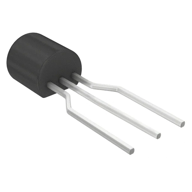


 工商网监
湘ICP备2023018690号
工商网监
湘ICP备2023018690号
