CAT4003B, CAT4004B
LED Driver, Constant
Current Programmable, with
32 Dimming Levels
Description
http://onsemi.com
The CAT4003B and CAT4004B provide respectively three and four
matched low dropout current sources to drive LEDs. The CAT400XB
requires no external RSET resistor. The LED current is internally set
to 25 mA when the device is first enabled. Each LED channel includes
an individual control loop allowing the device to handle a wide range
of LED forward voltages while still maintaining tight current
matching.
The EN/DIM logic input supports the device enable and a digital
dimming interface for setting the LED channel current with 32 linear
dimming levels.
LEDs can be powered directly from a Lithium−ion battery due to the
low dropout (75 mV at 20 mA) current sinks.
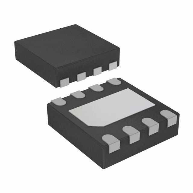
Package options are available in the 4−channel tiny 8−pad UDFN 2
mm x 2 mm with a max height of 0.55 mm, and 3− channel in the 6
−lead TSOT−23, TSOP and SC−70.
Features
•
•
•
•
•
•
•
•
•
•
3, 4 LED Current Sinks with Tight Matching
32 Dimming Levels
Low Dropout Driver 75 mV at 20 mA
No Switching Noise
Shutdown Current less than 1 mA
25 mA Max LED Current per Channel
Dimming via 1−wire EZDim Interface
Thermal Shutdown Protection
RoHS Compliant
6−lead TSOT−23, TSOP, SC−70, and 8−pad UDFN 2 mm x 2 mm
Packages
Typical Applications
• LCD Display Backlight
• Cellular Phones
• Digital Still Cameras
UDFN−8
HU2 SUFFIX
CASE 517AW
TSOT23−6
TD SUFFIX
CASE 419AF
SC70−6
SD SUFFIX
CASE 419AD
TSOP−6
TS SUFFIX
CASE 318G
TYPICAL APPLICATION CIRCUIT
VIN
2.4 V CIN
to
5.5 V 1 mF
LED1 LED2
LED3
VIN
CAT4003B
One Wire
Programming
32 Steps
EN/DIM
GND
This document contains information on some products that are still under development.
ON Semiconductor reserves the right to change or discontinue these products without
notice.
ORDERING INFORMATION
See detailed ordering information on page 2 of this data
sheet.
© Semiconductor Components Industries, LLC, 2011
January, 2012 − Rev. 2
1
Publication Order Number:
CAT4003B/D
�CAT4003B, CAT4004B
MARKING DIAGRAMS
BH
A
Y
M
BHA
YM
KLYM
UDFN8 (2 x 2 mm)
TSOT23−6L
= CAT4004B Device Code
= Assembly Location Code
= Production Year (last digit)
= Production Month: 1 − 9, O, N, D
KL
Y
M
= CAT4003B Device Code
= Production Year (last digit)
= Production Month: 1 − 9, O, N, D
KLA
L4AYW
SC70−6L
KL
A
TSOP−6
= CAT4003B Device Code
= Assembly Location Code
L4 = CAT4003B Device Code
A
= Assembly Location Code
YW = Year and Work Week
ORDERING INFORMATION (Note 1)
Orderable Part Number
CAT4003BTD−GT3
Package
Finish
Shipping (Note 2)
TSOT−23, 6−Lead
NiPdAu (RoHS Compliant)
3,000 / Tape & Reel
CAT4003BTS−T3
TSOP, 6−Lead
Matte−Tin (RoHS Compliant)
3,000 / Tape & Reel
CAT4003BSD−GT3
SC−70, 6−Lead
NiPdAu (RoHS Compliant)
3,000 / Tape & Reel
UDFN, 8−Pad, 2 x 2 mm
NiPdAu (RoHS Compliant)
3,000 / Tape & Reel
CAT4004BHU2−GT3
1. For additional package and temperature options, please contact your nearest ON Semiconductor Sales office.
2. For information on tape and reel specifications, including part orientation and tape sizes, please refer to our Tape and Reel Packaging
Specifications Brochure, BRD8011/D.
3. For detailed information and a breakdown of device nomenclature and numbering systems, please see the ON Semiconductor Device
Nomenclature document, TND310/D, available at www.onsemi.com
http://onsemi.com
2
�CAT4003B, CAT4004B
PIN CONNECTIONS (Top View)
1
1
EN/DIM
GND
LED1
LED2
VIN
NC
LED4
LED3
EN/DIM
LED1
LED1
GND
LED2
GND
VIN
LED3
EN/DIM
CAT4004B
UDFN8 2 x 2 mm
CAT4003B
TSOT23−6L, TSOP−6
1
LED2
LED3
VIN
CAT4003B
SC70−6L
Table 1. PIN FUNCTIONS
Pin Name
Function
EN/DIM
Device Enable (active high) and Dimming Control
GND
Ground Reference
LED1
LED1 Cathode Terminal
LED2
LED2 Cathode Terminal
LED3
LED3 Cathode Terminal
LED4
LED4 Cathode Terminal
VIN
Device Supply Input, Connect to Battery or Supply
TAB
Connect to GND on the PCB, for CAT4004B only.
Table 2. ABSOLUTE MAXIMUM RATINGS
Parameter
Value
Unit
6
V
VIN + 0.7
V
Storage Temperature Range
−65 to +150
°C
Junction Temperature Range
−40 to +125
°C
300
°C
VIN, LEDx Voltage
EN/DIM Voltage
Lead Temperature
Stresses exceeding Maximum Ratings may damage the device. Maximum Ratings are stress ratings only. Functional operation above the
Recommended Operating Conditions is not implied. Extended exposure to stresses above the Recommended Operating Conditions may affect
device reliability.
Table 3. RECOMMENDED OPERATING CONDITIONS
Parameter
Value
Unit
VIN
2.4 to 5.5
V
Ambient Temperature Range
−40 to +85
°C
0 to 25
mA
LED Current Range
4. Typical application circuit with external components is shown on page 1.
http://onsemi.com
3
�CAT4003B, CAT4004B
Table 4. ELECTRICAL OPERATING CHARACTERISTICS
(over recommended operating conditions unless specified otherwise) (VIN = 4.0 V, EN = High, TAMB = 25°C) (Note 6)
Conditions
Symbol
Min
Typ
Max
Units
Quiescent Current
ILED = 25 mA/channel
IQ
0.5
0.7
1.5
mA
Shutdown Current
VEN = 0 V
IQSHDN
1
mA
Parameter
Full Scale LED Current (Average) (Note 5)
LED Channel Matching
Dropout Voltage
ILED−FULL
24
25
26
mA
I LED * I LEDAVG
I LEDAVG
ILED−DEV
−5
±1
+5
%
ILED = 20 mA
ILED = 1 mA
VDOUT
EN/DIM Pin
− Internal pull−down resistor
− Logic High Level
− Logic Low Level
REN/DIM
VHI
VLO
75
45
mV
200
kW
V
V
1.3
0.4
Thermal Shutdown
TSD
150
°C
Thermal Hysteresis
THYS
20
°C
Undervoltage lockout (UVLO) threshold
VUVLO
2.0
V
5. For the CAT4003B, ILEDAVG = (ILED,CH1 + ILED,CH2 + ILED,CH3) / 3
6. The Min/Max limits apply across the −40°C to +85°C ambient temperature range and are assured by design, characterization and correlation
with statistical analysis.
Table 5. RECOMMENDED EN/DIM TIMING (For 3 V ≤ VIN ≤ 5.5 V, over full ambient temperature range −40°C to +85°C.) (Note 7)
Parameter
Conditions
Symbol
Min
TSETUP
10
EN/DIM program low time
TLO
0.2
EN/DIM program high time
THI
0.2
Power−up Setup Time
LED current settling time
Typ
TLED
EN/DIM low time to shutdown
Max
ms
500
2
ms
ms
10
TPWRDWN
Units
3
ms
5
ms
7. The Min/Max limits apply across the −40°C to +85°C ambient temperature range and are assured by design, characterization and correlation
with statistical analysis.
THI
EN/DIM
TSETUP
TLED
100%
LED
Current
TPWRDWN
TLO
100%
97% 94%
32 Levels
Shutdown
3%
0%
Shutdown
Figure 1. CAT400XB EN/DIM Dimming Timing Diagram
LED Current Setting
consecutive rising edge on the EN/DIM decreases the LED
current by one step until it goes to zero, as shown on
Figure 1.
On the CAT400XB, the full scale LED current is
internally set to 25 mA (no external resistor).
When the EN/DIM is first enabled, the CAT400XB sets
the LED channel current to the full scale current. Each
http://onsemi.com
4
�CAT4003B, CAT4004B
TYPICAL CHARACTERISTICS
(CAT4003B, VIN = 4 V, VF = 3.3 V, IOUT = 75 mA (3 LEDs at 25 mA), CIN = 1 μF, TAMB = 25°C unless otherwise specified.)
1.4
−40°C
1.2
QUIESCENT CURRENT [mA]
ENABLE HIGH THRESHOLD [V]
1.4
25°C
1.0
0.8
0.6
80°C
0.4
1.2
1.0
0.8
0.6
2.0 2.5
3.0
3.5
4.0
4.5
5.0
5.5
2.5 3.0
1.0
10
0.8
8
0.6
0.4
0.2
0.0
−0.2
−0.4
−0.6
3.5
4.0
4.5
4.5
5.0
5.5
Figure 3. Quiescent Current vs. Input Voltage
(full load)
LED CURRENT CHANGE [%]
LED CURRENT CHANGE [%]
Figure 2. EN High Threshold vs. Input Voltage
2.5 3.0
4.0
INPUT VOLTAGE [V]
INPUT VOLTAGE [V]
−0.8
−1.0
3.5
5.0
5.5
6
4
2
0
−2
−4
−6
−8
−10
−40
INPUT VOLTAGE [V]
0
40
80
120
TEMPERATURE [°C]
Figure 4. LED Current Change vs. Input Voltage
Figure 5. LED Current Change vs. Temperature
http://onsemi.com
5
�CAT4003B, CAT4004B
TYPICAL CHARACTERISTICS
(CAT4003B, VIN = 4 V, VF = 3.3 V, IOUT = 75 mA (3 LEDs at 25 mA), CIN = 1 μF, TAMB = 25°C unless otherwise specified.)
30
100
25mA
90
20
EFFICIENCY [%]
LED CURRENT [mA]
25
15
10
5
0
0.8mA
0
50
100
150
200
250
80
70
60
50
300
LED PIN VOLTAGE [mV]
3.0
3.5
4.0
4.5
5.0
INPUT VOLTAGE [V]
Figure 6. Dropout Characteristics
Figure 7. Efficiency vs. Input Voltage
Figure 8. Power Up Waveform
Figure 9. Power Down Waveform
Figure 10. Line Transient Waveform
Figure 11. Dimming Levels
http://onsemi.com
6
�CAT4003B, CAT4004B
Pin Functions
into “zero current” shutdown mode, the EN/DIM pin must
be held low for 3 ms typical
LED1 to LED4 provide the internal regulated current for
each of the LED cathodes. The pins enter a high impedance
zero current state whenever the device is placed in shutdown
mode.
GND is the ground reference for the device. The pin must be
connected to the ground plane on the PCB.
TAB (CAT4004B only) is the exposed pad underneath the
package. For best thermal performance, the tab should be
soldered to the PCB and connected to the ground plane.
VIN is the supply pin for the charge pump. A small 1 mF
ceramic bypass capacitor is required between the VIN pin
and ground near the device. The operating input voltage
range is from 2.4 V to 5.5 V. Whenever the input supply falls
below the under−voltage threshold (2.0 V), all the LED
channels are disabled and the device enters shutdown mode.
EN/DIM is the enable and one wire dimming input for all
LED channels. Levels of logic high and logic low are set at
1.3 V and 0.4 V respectively. When EN/DIM is initially
taken high, the CAT400XB becomes enabled and all LED
currents are set to the full scale 25 mA. To place the device
LED4
LED3
Undervoltage
Lockout
VIN
LED2
LED1
VIN
Reference
Voltage
Current
Setting DAC
EN/DIM
Serial
Interface
4 Current Sink
Regulators
Register
200 kΩ
GND
Figure 12. CAT4004B Functional Block Diagram
Basic Operation
The full scale current is calculated from the above formula
with n equal to zero.
The EN/DIM pin has two primary functions. One function
enables and disables the device. The other function is LED
current dimming with 32 different levels by pulsing the input
signal, as shown on Figure 1. On each successive pulse
rising edge, the LED current is decreased by about 3.2%
(1/31st of the full scale value). After 30 pulses, the LED
current is 3.2% of the full scale current. On the 31st pulse, the
current drops to zero, and then goes back to full scale on the
following pulse.
Initially once the EN/DIM input is first pulled high, it
must remain high for at least TSETUP delay (10 ms minimum)
to allow the LED driver to complete its power−up. After this
delay, EN/DIM can be pulsed in order to set the LED current
to the desired level. Each pulse width should be between
1 ms and 500 ms. Pulses faster than the minimum TLO may
be ignored and filtered by the device. Pulses longer than the
maximum TLO may shutdown the device. By pulsing the
EN/DIM signal at a high frequency, the LED current can
quickly be set to zero or to any other level.
The CAT400XB uses tightly matched current sinks to
accurately regulate LED current in each channel.
There are 32 different settings for LED brightness that can
be programmed through the EN/DIM pin. Tight current
regulation for all channels is possible over a wide range of
input and LED voltages due to independent current sensing
circuitry on each channel.
Each LED channel needs a minimum of 75 mV headroom
to sink a constant regulated current of 20 mA. If the input
supply falls below 2.0 V, the under−voltage lockout circuit
disables all LED channels and resets the circuit to default
values. Any unused LED channels should be left open.
CAT400XB LED Current Selection
After power−up and once enabled, the LED current is set
initially to the full scale currrent of 25 mA. The number of
pulses (n) on the EN/DIM input does decrease the current
value as follows:
LED current [mA] + 25
ǒ3131* nǓ
http://onsemi.com
7
�CAT4003B, CAT4004B
The LED driver enters a “zero current” shutdown mode if
EN/DIM is held low for longer than 5 ms.
The dimming level is set by the number of pulses on the
EN/DIM after the power−up, as shown in Table 6.
Full Scale Current in %
Dimming Pulses [n]
55
14
52
15
48
16
45
17
Dimming Pulses [n]
42
18
100
0
39
19
97
1
35
20
94
2
32
21
90
3
29
22
87
4
26
23
84
5
23
24
81
6
19
25
77
7
16
26
74
8
13
27
71
9
10
28
68
10
6
29
65
11
3
30
61
12
0
31
13
100
32
Table 6. DIMMING LEVELS
Full Scale Current in %
58
http://onsemi.com
8
�MECHANICAL CASE OUTLINE
PACKAGE DIMENSIONS
TSOP−6
CASE 318G−02
ISSUE V
1
SCALE 2:1
D
H
ÉÉ
ÉÉ
6
E1
1
NOTE 5
5
2
L2
4
GAUGE
PLANE
E
3
L
b
SEATING
PLANE
C
DETAIL Z
e
DIM
A
A1
b
c
D
E
E1
e
L
L2
M
c
A
0.05
M
DATE 12 JUN 2012
NOTES:
1. DIMENSIONING AND TOLERANCING PER ASME Y14.5M, 1994.
2. CONTROLLING DIMENSION: MILLIMETERS.
3. MAXIMUM LEAD THICKNESS INCLUDES LEAD FINISH. MINIMUM
LEAD THICKNESS IS THE MINIMUM THICKNESS OF BASE MATERIAL.
4. DIMENSIONS D AND E1 DO NOT INCLUDE MOLD FLASH,
PROTRUSIONS, OR GATE BURRS. MOLD FLASH, PROTRUSIONS, OR
GATE BURRS SHALL NOT EXCEED 0.15 PER SIDE. DIMENSIONS D
AND E1 ARE DETERMINED AT DATUM H.
5. PIN ONE INDICATOR MUST BE LOCATED IN THE INDICATED ZONE.
A1
DETAIL Z
MIN
0.90
0.01
0.25
0.10
2.90
2.50
1.30
0.85
0.20
0°
MILLIMETERS
NOM
MAX
1.00
1.10
0.06
0.10
0.38
0.50
0.18
0.26
3.00
3.10
2.75
3.00
1.50
1.70
0.95
1.05
0.40
0.60
0.25 BSC
10°
−
STYLE 1:
PIN 1. DRAIN
2. DRAIN
3. GATE
4. SOURCE
5. DRAIN
6. DRAIN
STYLE 2:
PIN 1. EMITTER 2
2. BASE 1
3. COLLECTOR 1
4. EMITTER 1
5. BASE 2
6. COLLECTOR 2
STYLE 3:
PIN 1. ENABLE
2. N/C
3. R BOOST
4. Vz
5. V in
6. V out
STYLE 4:
PIN 1. N/C
2. V in
3. NOT USED
4. GROUND
5. ENABLE
6. LOAD
STYLE 5:
PIN 1. EMITTER 2
2. BASE 2
3. COLLECTOR 1
4. EMITTER 1
5. BASE 1
6. COLLECTOR 2
STYLE 6:
PIN 1. COLLECTOR
2. COLLECTOR
3. BASE
4. EMITTER
5. COLLECTOR
6. COLLECTOR
STYLE 7:
PIN 1. COLLECTOR
2. COLLECTOR
3. BASE
4. N/C
5. COLLECTOR
6. EMITTER
STYLE 8:
PIN 1. Vbus
2. D(in)
3. D(in)+
4. D(out)+
5. D(out)
6. GND
STYLE 9:
PIN 1. LOW VOLTAGE GATE
2. DRAIN
3. SOURCE
4. DRAIN
5. DRAIN
6. HIGH VOLTAGE GATE
STYLE 10:
PIN 1. D(OUT)+
2. GND
3. D(OUT)−
4. D(IN)−
5. VBUS
6. D(IN)+
STYLE 11:
PIN 1. SOURCE 1
2. DRAIN 2
3. DRAIN 2
4. SOURCE 2
5. GATE 1
6. DRAIN 1/GATE 2
STYLE 12:
PIN 1. I/O
2. GROUND
3. I/O
4. I/O
5. VCC
6. I/O
STYLE 13:
PIN 1. GATE 1
2. SOURCE 2
3. GATE 2
4. DRAIN 2
5. SOURCE 1
6. DRAIN 1
STYLE 14:
PIN 1. ANODE
2. SOURCE
3. GATE
4. CATHODE/DRAIN
5. CATHODE/DRAIN
6. CATHODE/DRAIN
STYLE 15:
PIN 1. ANODE
2. SOURCE
3. GATE
4. DRAIN
5. N/C
6. CATHODE
STYLE 16:
PIN 1. ANODE/CATHODE
2. BASE
3. EMITTER
4. COLLECTOR
5. ANODE
6. CATHODE
STYLE 17:
PIN 1. EMITTER
2. BASE
3. ANODE/CATHODE
4. ANODE
5. CATHODE
6. COLLECTOR
GENERIC
MARKING DIAGRAM*
RECOMMENDED
SOLDERING FOOTPRINT*
6X
0.60
XXXAYWG
G
1
6X
3.20
XXX
A
Y
W
G
0.95
PITCH
DIMENSIONS: MILLIMETERS
*For additional information on our Pb−Free strategy and soldering
details, please download the ON Semiconductor Soldering and
Mounting Techniques Reference Manual, SOLDERRM/D.
DOCUMENT NUMBER:
DESCRIPTION:
98ASB14888C
TSOP−6
1
IC
0.95
XXX MG
G
= Specific Device Code
=Assembly Location
= Year
= Work Week
= Pb−Free Package
STANDARD
XXX = Specific Device Code
M
= Date Code
G
= Pb−Free Package
*This information is generic. Please refer to device data sheet
for actual part marking. Pb−Free indicator, “G” or microdot “
G”, may or may not be present.
Electronic versions are uncontrolled except when accessed directly from the Document Repository.
Printed versions are uncontrolled except when stamped “CONTROLLED COPY” in red.
PAGE 1 OF 1
ON Semiconductor and
are trademarks of Semiconductor Components Industries, LLC dba ON Semiconductor or its subsidiaries in the United States and/or other countries.
ON Semiconductor reserves the right to make changes without further notice to any products herein. ON Semiconductor makes no warranty, representation or guarantee regarding
the suitability of its products for any particular purpose, nor does ON Semiconductor assume any liability arising out of the application or use of any product or circuit, and specifically
disclaims any and all liability, including without limitation special, consequential or incidental damages. ON Semiconductor does not convey any license under its patent rights nor the
rights of others.
© Semiconductor Components Industries, LLC, 2019
www.onsemi.com
�MECHANICAL CASE OUTLINE
PACKAGE DIMENSIONS
SC−88 (SC−70 6 Lead), 1.25x2
CASE 419AD
ISSUE A
DATE 07 JUL 2010
1
D
e
e
E1 E
SYMBOL
MIN
A
0.80
MAX
1.10
A1
0.00
0.10
A2
0.80
1.00
b
0.15
0.30
0.18
c
0.10
D
1.80
2.00
2.20
E
1.80
2.10
2.40
E1
1.15
1.25
1.35
0.65 BSC
e
L
0.26
L1
0.36
0.46
0.42 REF
0.15 BSC
L2
TOP VIEW
NOM
θ
0º
8º
θ1
4º
10º
q1
A2 A
q
b
q1
L
L1
A1
SIDE VIEW
c
L2
END VIEW
Notes:
(1) All dimensions are in millimeters. Angles in degrees.
(2) Complies with JEDEC MO-203.
DOCUMENT NUMBER:
DESCRIPTION:
98AON34266E
Electronic versions are uncontrolled except when accessed directly from the Document Repository.
Printed versions are uncontrolled except when stamped “CONTROLLED COPY” in red.
SC−88 (SC−70 6 LEAD), 1.25X2
PAGE 1 OF 1
onsemi and
are trademarks of Semiconductor Components Industries, LLC dba onsemi or its subsidiaries in the United States and/or other countries. onsemi reserves
the right to make changes without further notice to any products herein. onsemi makes no warranty, representation or guarantee regarding the suitability of its products for any particular
purpose, nor does onsemi assume any liability arising out of the application or use of any product or circuit, and specifically disclaims any and all liability, including without limitation
special, consequential or incidental damages. onsemi does not convey any license under its patent rights nor the rights of others.
© Semiconductor Components Industries, LLC, 2019
www.onsemi.com
�MECHANICAL CASE OUTLINE
PACKAGE DIMENSIONS
TSOT−23, 6 LEAD
CASE 419AF−01
ISSUE O
DATE 19 DEC 2008
SYMBOL
D
MIN
NOM
A
e
E1
MAX
1.00
A1
0.01
0.05
0.10
A2
0.80
0.87
0.90
b
0.30
c
0.12
E
0.45
0.15
D
2.90 BSC
E
2.80 BSC
E1
1.60 BSC
e
0.95 TYP
L
0.30
L1
0.40
0.20
0.50
0.60 REF
L2
0.25 BSC
0º
θ
8º
TOP VIEW
A2 A
b
q
L
A1
c
L2
L1
SIDE VIEW
END VIEW
Notes:
(1) All dimensions are in millimeters. Angles in degrees.
(2) Complies with JEDEC MO-193.
DOCUMENT NUMBER:
DESCRIPTION:
98AON34406E
TSOT−23, 6 LEAD
Electronic versions are uncontrolled except when accessed directly from the Document Repository.
Printed versions are uncontrolled except when stamped “CONTROLLED COPY” in red.
PAGE 1 OF 1
ON Semiconductor and
are trademarks of Semiconductor Components Industries, LLC dba ON Semiconductor or its subsidiaries in the United States and/or other countries.
ON Semiconductor reserves the right to make changes without further notice to any products herein. ON Semiconductor makes no warranty, representation or guarantee regarding
the suitability of its products for any particular purpose, nor does ON Semiconductor assume any liability arising out of the application or use of any product or circuit, and specifically
disclaims any and all liability, including without limitation special, consequential or incidental damages. ON Semiconductor does not convey any license under its patent rights nor the
rights of others.
© Semiconductor Components Industries, LLC, 2019
www.onsemi.com
�MECHANICAL CASE OUTLINE
PACKAGE DIMENSIONS
UDFN8, 2x2
CASE 517AW
ISSUE A
1
SCALE 2:1
ÇÇ
ÇÇ
E
DETAIL A
ALTERNATE
CONSTRUCTIONS
0.10 C
2X
L
L
L1
PIN ONE
REFERENCE
2X
B
A
D
DATE 13 NOV 2015
0.10 C
TOP VIEW
DETAIL B
A
0.10 C
A3
A1
0.08 C
A1
SIDE VIEW
NOTE 4
C
D2
DETAIL A
1
8X
4
SEATING
PLANE
5
e
e/2
A3
ALTERNATE
CONSTRUCTION
MILLIMETERS
MIN
MAX
0.45
0.55
0.00
0.05
0.13 REF
0.18
0.30
2.00 BSC
1.50
1.70
2.00 BSC
0.80
1.00
0.50 BSC
0.20
0.45
−−−
0.15
GENERIC
MARKING DIAGRAM*
8X
1
b
0.10 C A B
0.05 C
NOTE 3
BOTTOM VIEW
RECOMMENDED
SOLDERING FOOTPRINT*
1.73
PACKAGE
OUTLINE
DETAIL B
DIM
A
A1
A3
b
D
D2
E
E2
e
L
L1
L
E2
8
ÇÇ
ÇÇ
ÉÉ
MOLD CMPD
EXPOSED Cu
NOTES:
1. DIMENSIONING AND TOLERANCING PER
ASME Y14.5M, 1994.
2. CONTROLLING DIMENSION: MILLIMETERS.
3. DIMENSION b APPLIES TO PLATED TERMINALS AND IS MEASURED BETWEEN 0.15
AND 0.30 MM FROM THE TERMINAL TIP.
4. COPLANARITY APPLIES TO THE EXPOSED
PAD AS WELL AS THE TERMINALS.
5. FOR DEVICE OPN CONTAINING W OPTION,
DETAIL B ALTERNATE CONSTRUCTION IS
NOT APPLICABLE.
8X
0.50
XX MG
G
XX = Specific Device Code
M = Date Code
G
= Pb−Free Package
(Note: Microdot may be in either location)
*This information is generic. Please refer to
device data sheet for actual part marking.
Pb−Free indicator, “G” or microdot “ G”,
may or may not be present.
2.30
1.00
1
8X
0.50
PITCH
0.30
DIMENSIONS: MILLIMETERS
*For additional information on our Pb−Free strategy and soldering
details, please download the ON Semiconductor Soldering and
Mounting Techniques Reference Manual, SOLDERRM/D.
DOCUMENT NUMBER:
DESCRIPTION:
98AON34462E
UDFN8, 2X2
Electronic versions are uncontrolled except when accessed directly from the Document Repository.
Printed versions are uncontrolled except when stamped “CONTROLLED COPY” in red.
PAGE 1 OF 1
ON Semiconductor and
are trademarks of Semiconductor Components Industries, LLC dba ON Semiconductor or its subsidiaries in the United States and/or other countries.
ON Semiconductor reserves the right to make changes without further notice to any products herein. ON Semiconductor makes no warranty, representation or guarantee regarding
the suitability of its products for any particular purpose, nor does ON Semiconductor assume any liability arising out of the application or use of any product or circuit, and specifically
disclaims any and all liability, including without limitation special, consequential or incidental damages. ON Semiconductor does not convey any license under its patent rights nor the
rights of others.
© Semiconductor Components Industries, LLC, 2019
www.onsemi.com
�onsemi,
, and other names, marks, and brands are registered and/or common law trademarks of Semiconductor Components Industries, LLC dba “onsemi” or its affiliates
and/or subsidiaries in the United States and/or other countries. onsemi owns the rights to a number of patents, trademarks, copyrights, trade secrets, and other intellectual property.
A listing of onsemi’s product/patent coverage may be accessed at www.onsemi.com/site/pdf/Patent−Marking.pdf. onsemi reserves the right to make changes at any time to any
products or information herein, without notice. The information herein is provided “as−is” and onsemi makes no warranty, representation or guarantee regarding the accuracy of the
information, product features, availability, functionality, or suitability of its products for any particular purpose, nor does onsemi assume any liability arising out of the application or use
of any product or circuit, and specifically disclaims any and all liability, including without limitation special, consequential or incidental damages. Buyer is responsible for its products
and applications using onsemi products, including compliance with all laws, regulations and safety requirements or standards, regardless of any support or applications information
provided by onsemi. “Typical” parameters which may be provided in onsemi data sheets and/or specifications can and do vary in different applications and actual performance may
vary over time. All operating parameters, including “Typicals” must be validated for each customer application by customer’s technical experts. onsemi does not convey any license
under any of its intellectual property rights nor the rights of others. onsemi products are not designed, intended, or authorized for use as a critical component in life support systems
or any FDA Class 3 medical devices or medical devices with a same or similar classification in a foreign jurisdiction or any devices intended for implantation in the human body. Should
Buyer purchase or use onsemi products for any such unintended or unauthorized application, Buyer shall indemnify and hold onsemi and its officers, employees, subsidiaries, affiliates,
and distributors harmless against all claims, costs, damages, and expenses, and reasonable attorney fees arising out of, directly or indirectly, any claim of personal injury or death
associated with such unintended or unauthorized use, even if such claim alleges that onsemi was negligent regarding the design or manufacture of the part. onsemi is an Equal
Opportunity/Affirmative Action Employer. This literature is subject to all applicable copyright laws and is not for resale in any manner.
PUBLICATION ORDERING INFORMATION
LITERATURE FULFILLMENT:
Email Requests to: orderlit@onsemi.com
onsemi Website: www.onsemi.com
◊
TECHNICAL SUPPORT
North American Technical Support:
Voice Mail: 1 800−282−9855 Toll Free USA/Canada
Phone: 011 421 33 790 2910
Europe, Middle East and Africa Technical Support:
Phone: 00421 33 790 2910
For additional information, please contact your local Sales Representative
�


 工商网监
湘ICP备2023018690号
工商网监
湘ICP备2023018690号
