CAT4004 4-Channel Constant Current LED Driver with EZDim™
FEATURES
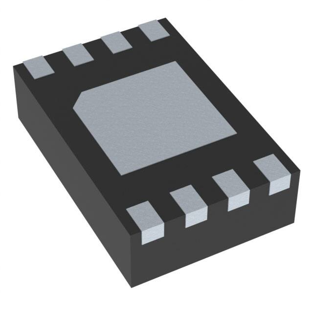
Four LED current sinks with tight matching Low Dropout Driver 130mV at 30mA No switching noise Shutdown current < 1μA LED current set by external resistor Dimming via 1-wire EZDimTM interface Thermal shutdown protection RoHS Compliant 8-lead 2mm x 3mm TDFN package
DESCRIPTION
The CAT4004 provides four matched low dropout current sources to drive LEDs. An external resistor on RSET sets the current in the LED channels. Each LED channel includes an individual control loop allowing the device to handle a wide range of LED forward voltages while still maintaining tight current matching. The EN/DIM logic inputs supports device enable and a digital dimming interface for current setting of all LEDs. Six different current dimming ratios are available. The device is aimed at “direct drive” battery applications. It is required that the battery or voltage source have enough headroom to drive the LED forward voltage and current sink (>150mV). The device is available in a tiny 8-lead TDFN 2mm x 3mm package with a max height of 0.8mm.
APPLICATIONS
LCD Display Backlight Cellular Phones Digital Still Cameras Handheld Devices
ORDERING INFORMATION
Part Number CAT4004VP2-T3 Package TDFN-8
(1)
Quantity per Reel 3000 3000
Package Marking FT HA
For Ordering Information details, see page 10.
CAT4004VP2-GT3 TDFN-8 (2)
Notes: (1) Matte-Tin Plated Finish (RoHS-compliant). (2) NiPdAu Plated Finish (RoHS-compliant).
PIN CONFIGURATION
8-lead TDFN Package
(Top View) EN/DIM 1 GND 2 LED1 3 LED2 4 CAT4004
8 VIN 7 RSET 6 LED4 5 LED3
TYPICAL APPLICATION CIRCUIT
VIN 2.4V to 5.5V CIN 1µF LED1 LED2 LED3 LED4 VIN One wire programming RSET 3.8kΩ EN/DIM RSET GND CAT4004 20mA
© 2008 SCILLC. All rights reserved. Characteristics subject to change without notice
1
Doc. No. MD-5024 Rev. C
�CAT4004 ABSOLUTE MAXIMUM RATINGS
Parameter VIN, LEDx, RSET EN/DIM Voltage Storage Temperature Range Junction Temperature Range Lead Temperature Rating 6 VIN + 0.7 -65 to +160 -40 to +150 300 Unit V V °C °C °C
RECOMMENDED OPERATING CONDITIONS
Parameter VIN Ambient Temperature Range ILED per LED pin Rating 2.4 to 5.5 0 to 40
(1)
Unit V °C mA
-40 to +85
Typical application circuit with external components is shown on page 1.
ELECTRICAL OPERATING CHARACTERISTICS
(over recommended operating conditions unless specified otherwise) VIN = 4.0V, EN = High, TAMB = 25°C Symbol IQ IQSHDN ILED-ACC ILED-DEV VDOUT REN/DIM VHI VLO TSD THYS VUVLO Name Quiescent Current Shutdown Current LED Current Accuracy LED Channel Matching Dropout Voltage EN/DIM Pin • Internal pull-down resistor • Logic High Level • Logic Low Level Thermal Shutdown Thermal Hysteresis Undervoltage lockout (UVLO) threshold Conditions No load, RSET = Float No load, RSET = 4.8kΩ VEN = 0V 1mA ≤ ILED ≤ 40mA ILED − ILEDAVG ILED ILED = 30mA Min Typ 0.6 1.0 1 ±1 -5 ±1 130 100 1.3 0.4 150 20 1.8 +5 Max Units mA mA µA % % mV kΩ V V °C °C V
Doc. No. MD-5024 Rev. C
2
© 2008 SCILLC. All rights reserved. Characteristics subject to change without notice
�CAT4004 RECOMMENDED EN/DIM TIMING
For 2.4 ≤ VIN ≤ 5.5V, over full ambient temperature range -40ºC to +85ºC. Symbol TSETUP TLO THI TPWRDWN TLED Name EN/DIM setup from shutdown EN/DIM program low time EN/DIM program high time EN/DIM low time to shutdown LED current settling time
TSETUP THI
Conditions
Min 10 0.2 0.2 1.5
Typ
Max 100
Units μs μs μs ms
40
TPWRDWN
μs
EN/DIM TLED 100% 50% LED Current Shutdown 25% TLO 100%
12.5% 6.25% 3.12%
Shutdown
Figure 1. EN/DIM Dimming Timing Diagram
EN/DIM number of pulses * LOW Transitions HIGH 1 2 3
st nd rd th
RSET Gain Shutdown mode 132 66 33 16.5 8.25 4.125 132 Device will keep cycling through gain selection
LED Current Zero 132 x 0.6V/RSET 66 x 0.6V/RSET 33 x 0.6V/RSET 16.5 x 0.6V/RSET 8.25 x 0.6V/RSET 4.125 x 0.6V/RSET 132 x 0.6V/RSET GAIN x 0.6V/RSET
4
5th 6th x
th
* The gain is changed on the rising edges of the EN/DIM input.
LED CURRENT SELECTION
At power-up, the initial LED current is set to full scale (100% brightness) by the external resistor RSET as follows: 0 .6 V LED current = 132 × R SET The EN/DIM pin has two primary functions. One function enables and disables the device. The other function is LED current dimming with six different levels by pulsing the input signal, as shown on Figure 3. On each consecutive pulse rising edge, the LED current is divided by half to 50%, then 25%, 12.5%, 6.25% and 3.125% dimming levels. Pulses faster than the minimum TLO may be ignored and filtered by the device. Pulses longer than the maximum TLO may shutdown the device. The LED driver enters a “zero current” shutdown mode if EN/DIM is held low for 1.5ms or more.
© 2008 SCILLC. All rights reserved. Characteristics subject to change without notice
3
Doc. No. MD-5024 Rev. C
�CAT4004 TYPICAL PERFORMANCE CHARACTERISTICS
VIN = 4V, VF = 3.3V, IOUT = 80mA (4 LEDs at 20mA), CIN = 1μF, TAMB = 25°C unless otherwise specified. Quiescent Current vs. Input Voltage
1.4 QUIESCENT CURRENT [mA]
QUIESCENT CURRENT [mA]
Quiescent Current vs. Temperature
1.4 1.2 1.0
1.2
1.0 0.8
0.8 0.6 -40 0 40 80 TEMPERATURE [°C] 120
0.6 2.5 3.0 3.5 4.0 4.5 5.0 INPUT VOLTAGE [V] 5.5
LED Current Change vs. Input Voltage
LED CURRENT CHANGE [%]
LED CURRENT CHANGE [%]
LED Current Change vs. Temperature
10 8 6 4 2 0 -2 -4 -6 -8 -10 -40 0 40 80 TEMPERATURE [°C] 120
1.0 0.8 0.6 0.4 0.2 0.0 -0.2 -0.4 -0.6 -0.8 -1.0 3.0 3.5 4.0 4.5 5.0 INPUT VOLTAGE [V] 5.5
LED Current vs. RSET Resistor
40 LED CURRENT [mA]
30
20
10
0 0 5 10 RSET [k Ω ] 15 20
Doc. No. MD-5024 Rev. C
4
© 2008 SCILLC. All rights reserved. Characteristics subject to change without notice
�CAT4004 TYPICAL PERFORMANCE CHARACTERISTICS
VIN = 4V, VF = 3.3V, IOUT = 80mA (4 LEDs at 20mA), CIN = 1μF, TAMB = 25°C unless otherwise specified. RSET Pin Voltage vs. Input Voltage
0.7 RSET VOLTAGE [V]
RSET VOLTAGE [V]
RSET Pin Voltage vs. Temperature
0.7 0.6 0.5 0.4 0.3 0.2
0.6 0.5 0.4 0.3 0.2 2.0 2.5 3.0 3.5 4.0 4.5 5.0 5.5 INPUT VOLTAGE [V]
-40
0 40 80 TEMPERATURE [°C]
120
LED Current vs. LED Pin Voltage
40 LED CURRENT [mA]
LED CURRENT [mA] 40
Dropout Characteristics
30
30
20
20
10
10
0 0.0 0.5 1.0 1.5 2.0 2.5 3.0 3.5 LED PIN VOLTAGE [V]
0 0 50 100 150 200 250 LED PIN VOLTAGE [mV] 300
Efficiency vs. Input Voltage
100 90 EFFICIENCY [%] 80 70 60 50 5.0 4.5 4.0 3.5 3.0 2.5 INPUT VOLTAGE [V] 2.0
© 2008 SCILLC. All rights reserved. Characteristics subject to change without notice
5
Doc. No. MD-5024 Rev. C
�CAT4004 TYPICAL PERFORMANCE CHARACTERISTICS
VIN = 4V, VF = 3.3V, IOUT = 80mA (4 LEDs at 20mA), CIN = 1μF, TAMB = 25°C unless otherwise specified. Power Up Waveform Power Down Waveform
Line Transient Waveform 4V to 5.5V
Dimming Waveform 80mA to 40mA
Doc. No. MD-5024 Rev. C
6
© 2008 SCILLC. All rights reserved. Characteristics subject to change without notice
�CAT4004 PIN DESCRIPTIONS
Pin # 1 2 3 4 5 6 7 8 TAB Name EN/DIM GND LED1 LED2 LED3 LED4 RSET VIN TAB Function Device enable (active high) and dimming control Ground reference LED1 cathode terminal LED2 cathode terminal LED3 cathode terminal LED4 cathode terminal RSET external LED mirror gain 128 Device supply input, connect to battery or supply Connect to GND on the PCB
PIN FUNCTION
VIN is the supply pin for the device logic. A small 1μF ceramic bypass capacitor is required between the VIN pin and ground near the device. The operating input voltage range is from 2.5V to 5.5V. Whenever the input supply falls below the under-voltage threshold (1.8V), all the LED channels are disabled and the device enters shutdown mode. EN/DIM is the enable and one wire dimming input for all LED channels. Levels of logic high and logic low are set at 1.3V and 0.4V respectively. When EN/DIM is initially taken high, the device becomes enabled and all LED currents are set to the full scale according to the resistor RSET. To place the device into “zero current” shutdown mode, the EN/DIM pin must be held low for at least 1.5ms. LED1 to LED4 provide the internal regulated current for each of the LED cathodes. There pins enter a high impedance zero current state whenver the device is placed in shutdown mode. RSET is connected to the resistor (RSET) to set the full scale current for the LEDs. The voltage at this pin is regulated to 0.6V. The ground side of the external resistor should be star connected back to the GND of the PCB. In shutdown mode, RSET beomes high impedance. GND is the ground reference for the device. The pin must be connected to the ground plane on the PCB. TAB is the exposed pad underneath the package. For best thermal performance, the tab should be soldered to the PCB and connected to the ground plane.
© 2008 SCILLC. All rights reserved. Characteristics subject to change without notice
7
Doc. No. MD-5024 Rev. C
�CAT4004 BLOCK DIAGRAM
VIN
LED1
LED2
LED3
VIN
Undervoltage Lockout Reference Voltage
RSET
Current Setting DAC
EN/DIM
Serial Interface 100kΩ
Register
4 Current Sink Regulators
GND
Figure 2. CAT4004 Functional Block Diagram
BASIC OPERATION
The CAT4004 uses four tightly matched current sinks to accurately regulate LED current in each channel proportional to the current sourced from the RSET pin.
ILED = GAIN × 0.6 V R SET
Each LED channel needs a minimum of 150mV headroom to sink constant regulated current. If the input supply falls below 1.8V, the under-voltage lockout circuit disables all LED channels and resets the circuit to default values. Any unused LED channels should be left open.
There are six different gain settings for LED brightness that can be set through the EN/DIM pin. The default gain on power-up is 132. Tight current regulation for all channels is possible over a wide range of input and LED voltages due to independent current sensing circuitry on each channel.
Doc. No. MD-5024 Rev. C
8
LED4
© 2008 SCILLC. All rights reserved. Characteristics subject to change without notice
�CAT4004 PACKAGE OUTLINE DRAWING
TDFN 8-Pad 2 x 3mm (VP2) (1)(2)
D
A
e
b
E
E2 PIN#1 IDENTIFICATION
A1 PIN#1 INDEX AREA D2 L
TOP VIEW
SIDE VIEW
BOTTOM VIEW
SYMBO L A A1 A2 A3 b D D2 E E2 e L
MIN 0.70 0.00 0.45 0.20 1.90 1.30 2.90 1.20 0.20
NOM 0.75 0.02 0.55 0.20 REF 0.25 2.00 1.40 3.00 1.30 050 TYP 0.30
MAX 0.80 0.05 0.65 0.30 2.10 1.50 3.10 1.40 0.40
A2 A3
FRONT VIEW
For current Tape & Reel information, download the pdf file from: http://www.catsemi.com/documents/tapeandreel.pdf
Notes: (1) All dimensions are in millimeters. (2) Complies with JEDEC standard MO-229.
© 2008 SCILLC. All rights reserved. Characteristics subject to change without notice
9
Doc. No. MD-5024 Rev. C
�CAT4004 EXAMPLE OF ORDERING INFORMATION1
Prefix CAT
Device # 4004
Suffix VP2 – G T2
Product Number 4004 Optional Company ID Package VP2: TDFN 2 x 3mm
Lead Finish G: NiPdAu Blank: Matte-Tin(4)
Tape & Reel T: Tape & Reel 3: 3000/Reel
Notes: (1) All packages are RoHS-compliant (Lead-free, Halogen-free). (2) The standard lead finish is NiPdAu. (3) The device used in the above example is a CAT4004VP2-GT3 (TDFN, NiPdAu Plated Finish, Tape & Reel 3000). (4) For Matte-Tin package option, please contact your nearest ON Semiconductor Sales office.
Doc. No. MD-5024 Rev. C
10
© 2008 SCILLC. All rights reserved. Characteristics subject to change without notice
�CAT4004 REVISION HISTORY
Date 15-Mar-07 Rev. A Reason Initial Issue Add NiPdAu lead finish Add Extended Temperature range Update Package Outline Drawing Update Example of Ordering Information Add “MD-” to Document Number Change logo and fine print to ON Semiconductor
07-Jan-08
B
17-Nov-08
C
ON Semiconductor and are registered trademarks of Semiconductor Components Industries, LLC (SCILLC). SCILLC reserves the right to make changes without further notice to any products herein. SCILLC makes no warranty, representation or guarantee regarding the suitability of its products for any particular purpose, nor does SCILLC assume any liability arising out of the application or use of any product or circuit, and specifically disclaims any and all liability, including without limitation special, consequential or incidental damages. “Typical” parameters which may be provided in SCILLC data sheets and/or specifications can and do vary in different applications and actual performance may vary over time. All operating parameters, including “Typicals” must be validated for each customer application by customer's technical experts. SCILLC does not convey any license under its patent rights nor the rights of others. SCILLC products are not designed, intended, or authorized for use as components in systems intended for surgical implant into the body, or other applications intended to support or sustain life, or for any other application in which the failure of the SCILLC product could create a situation where personal injury or death may occur. Should Buyer purchase or use SCILLC products for any such unintended or unauthorized application, Buyer shall indemnify and hold SCILLC and its officers, employees, subsidiaries, affiliates, and distributors harmless against all claims, costs, damages, and expenses, and reasonable attorney fees arising out of, directly or indirectly, any claim of personal injury or death associated with such unintended or unauthorized use, even if such claim alleges that SCILLC was negligent regarding the design or manufacture of the part. SCILLC is an Equal Opportunity/Affirmative Action Employer. This literature is subject to all applicable copyright laws and is not for resale in any manner.
PUBLICATION ORDERING INFORMATION
LITERATURE FULFILLMENT: Literature Distribution Center for ON Semiconductor P.O. Box 5163, Denver, Colorado 80217 USA Phone: 303-675-2175 or 800-344-3860 Toll Free USA/Canada Fax: 303-675-2176 or 800-344-3867 Toll Free USA/Canada Email: orderlit@onsemi.com N. American Technical Support: 800-282-9855 Toll Free USA/Canada Europe, Middle East and Africa Technical Support: Phone: 421 33 790 2910 Japan Customer Focus Center: Phone: 81-3-5773-3850 ON Semiconductor Website: www.onsemi.com Order Literature: http://www.onsemi.com/orderlit For additional information, please contact your local Sales Representative
© 2008 SCILLC. All rights reserved. Characteristics subject to change without notice
11
Doc. No. MD-5024 Rev. C
�


 工商网监
湘ICP备2023018690号
工商网监
湘ICP备2023018690号
