CS8151
5.0 V, 100 mA Low Dropout
Linear Regulator with
Watchdog, RESET,
and Wake Up
The CS8151 is a precision 5.0 V, 100 mA micro−power voltage
regulator with very low quiescent current (400 mA typical at 200 mA
load). The 5.0 V output is accurate within ±2% and supplies 100 mA
of load current with a typical dropout voltage of 400 mV.
Microprocessor control logic includes Watchdog, Wake Up and
RESET. This unique combination of low quiescent current and full
microprocessor control makes the CS8151 ideal for use in battery
operated, microprocessor controlled equipment.
The CS8151 Wake Up function brings the microprocessor out of
Sleep mode. The microprocessor in turn, signals its Wake Up status
back to the CS8151 by issuing a Watchdog signal.
The Watchdog logic function monitors an input signal (WDI) from
the microprocessor. The CS8151 responds to the falling edge of the
Watchdog signal which it expects at least once during each wake−up
period. When the correct Watchdog signal is received, a falling edge is
issued on the wake−up signal line.
RESET is independent of VIN and operates correctly to an output
voltage as low as 1.0 V. A RESET signal is issued in any of three
situations. During power up the RESET is held low until the output
voltage is in regulation. During operation if the output voltage shifts
below the regulation limits, the RESET toggles low and remains low
until proper output voltage regulation is restored. And finally, a
RESET signal is issued if the regulator does not receive a Watchdog
signal within the Wake Up period.
The RESET pulse width, Wake Up signal frequency, and Wake Up
delay time are all set by one external capacitor CDelay.
The regulator is protected against short circuit, over voltage, and
thermal runaway conditions. The device can withstand 74 V peak
transients, making it suitable for use in automotive environments.
http://onsemi.com
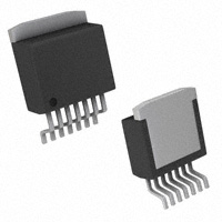
D2PAK−7
DPS SUFFIX
CASE 936AB
1
7
SO−16L
DWF SUFFIX
CASE 751G
16
1
SOIC−14
D SUFFIX
CASE 751A
14
1
DEVICE MARKING INFORMATION
See general marking information in the device marking
section on page 2 of this data sheet.
ORDERING INFORMATION
See detailed ordering and shipping information in the package
dimensions section on page 11 of this data sheet.
Features
• 5.0 V ± 2%/100 mA Output Voltage
• Micropower Compatible Control Functions
Wake Up
Watchdog
♦ RESET
Low Dropout Voltage: 400 mV @ 100 mA
Low Sleep Mode Quiescent Current (400 mA Typ)
Protection Features
♦ Thermal Shutdown
♦ Short Circuit
♦ 74 V Peak Transient Capability
♦ Reverse Transient (−50 V)
Internally Fused Leads in SO−14L and SO−16L Packages
These are Pb−Free Devices
♦
♦
•
•
•
•
•
© Semiconductor Components Industries, LLC, 2008
October, 2008 − Rev. 18
1
Publication Order Number:
CS8151/D
�CS8151
PIN CONNECTIONS AND MARKING DIAGRAMS
CS
8151
AWLYWWG
1
Tab = GND
Pin 1. VOUT
2. VIN
3. WDI
4. GND
5. Wake Up
6. RESET
7. Delay
SO−16L
CASE 751G
RESET
Wake Up
GND
GND
GND
WDI
VIN
A
WL
Y, YY
WW
G
NC
NC
NC
GND
GND
GND
Sense
VOUT
1
16
CS8151
AWLYYWWG
Delay
NC
GND
GND
GND
Sense
VOUT
SO−14L
CASE 751A
1
14
CS8151G
AWLYWW
D2PAK−7
CASE 936AB
Delay
RESET
Wake Up
GND
GND
WDI
NC
VIN
= Assembly Location
= Wafer Lot
= Year
= Work Week
= Pb−Free Package
VOUT
VIN
Current Source
(Circuit Bias)
Delay
Overvoltage
Shutdown
Current
Limit
Sense
Timing
Circuit
Wake Up
Circuit
+ −
Watchdog
Circuit
WDI
VOUT
Internally
connected
on D2PAK
Wake Up
Sense
Error
Amplifier
Thermal
Shutdown
Falling Edge
Detector
Bandgap
Reference
VOUT
RESET
RESET
Circuit
GND
Figure 1. Block Diagram
http://onsemi.com
2
�CS8151
MAXIMUM RATINGS*
Rating
Value
Unit
Power Dissipation
Internally Limited
−
Output Current (VOUT, RESET, Wake Up)
Internally Limited
−
Reverse Battery
−15
V
Peak Transient Voltage (60 V Load Dump @ VIN = 14 V)
+74
V
Maximum Negative Transient (t < 2.0 ms)
−50
V
ESD Susceptibility (Human Body Model)
2.0
kV
ESD Susceptibility (Machine Model)
200
V
Logic Inputs/Outputs
−0.3 to +6.0
V
Storage Temperature Range
−55 to +150
°C
260 peak
240 peak
°C
°C
Lead Temperature Soldering
Wave Solder (through hole styles only) (Note 1)
Reflow (SMD styles only) (Notes 2 & 3)
Stresses exceeding Maximum Ratings may damage the device. Maximum Ratings are stress ratings only. Functional operation above the
Recommended Operating Conditions is not implied. Extended exposure to stresses above the Recommended Operating Conditions may affect
device reliability.
1. 10 seconds max
2. 60 seconds max above 183°C
3. −5°C / +0°C allowable conditions
*The maximum package power dissipation must be observed
ELECTRICAL CHARACTERISTICS (−40°C ≤ TA ≤ 125°C, −40°C ≤ TJ ≤ 150°C, 6.0 V ≤ VIN ≤ 26 V, 100 mA ≤ IOUT ≤ 100 mA,
C2 = 47 mF (ESR < 8.0 W), CDelay = 0.1 mF; unless otherwise specified.)
Characteristic
Test Conditions
Min
Typ
Max
Unit
4.90
4.85
5.0
5.0
5.10
5.15
V
V
Output Section
Output Voltage, VOUT
9.0 V < VIN < 16 V
6.0 V < VIN < 26 V, 0 < IOUT < 100 mA
Dropout Voltage (VIN − VOUT)
IOUT = 100 mA
IOUT = 100 mA
−
−
400
100
600
150
mV
mV
Load Regulation
VIN = 14 V, 100 mA < IOUT < 100 mA
−
10
50
mV
Line Regulation
IOUT = 1.0 mA, 6.0 V < VIN < 26 V
−
10
50
mV
Ripple Rejection
7.0 V < VIN < 17 V @ f = 120 Hz, IOUT = 100 mA
60
75
−
dB
Current Limit
VOUT = 4.5 V
100
250
−
mA
150
180
210
°C
Thermal Shutdown
−
Overvoltage Shutdown
VOUT < 1.0 V
50
56
62
V
Quiescent Current
IOUT = 200 mA (Sleep)
IOUT = 50 mA
IOUT = 100 mA (Wake Up)
−
−
−
0.4
4.0
12
0.75
−
20
mA
mA
mA
Reverse Current
VOUT = 5.0 V, VIN = 0 V
−
1.0
1.5
mA
RESET
Threshold High (RTH)
RTH VOUT Increasing
VOUT − 0.3
−
VOUT − 0.04
V
Threshold Low (RTL)
RTL VOUT Decreasing
4.5
4.7
4.91
V
Hysteresis
RTH − RTL
150
200
250
mV
Output Low
1.0 V < VOUT RTL, IOUT = 25 mA
−
0.2
0.8
V
Output High
IOUT = 25 mA, VOUT > RTH
3.8
4.2
5.1
V
http://onsemi.com
3
�CS8151
ELECTRICAL CHARACTERISTICS (−40°C ≤ TA ≤ 125°C, −40°C ≤ TJ ≤ 150°C, 6.0 V ≤ VIN ≤ 26 V, 100 mA ≤ IOUT ≤ 100 mA,
C2 = 47 mF (ESR < 8.0 W), CDelay = 0.1 mF; unless otherwise specified.)
Characteristic
Test Conditions
Min
Typ
Max
Unit
0.025
0.1
0.5
12
1.30
80
mA
mA
3.0
5.0
7.0
ms
RESET
Current Limit
RESET = 0 V, VOUT > VRTH (Sourcing)
RESET = 5.0 V, VOUT > 1.0 V (Sinking)
Delay Time
POR Mode
Watchdog Input
Threshold High
−
−
1.4
2.0
V
Threshold Low
−
0.8
1.3
−
V
Hysteresis
−
25
100
−
mV
Input Current
0 < WDI < 6.0 V
−10
0
+10
mA
Pulse Width
50% WDI Falling Edge to
50% WDI Rising Edge and
50% WDI Rising Edge to
50% WDI Falling Edge
(see Figures 2, 3, and 4)
5.0
−
−
ms
Wake Up Period
See Figure 2
30
40
50
ms
Wake Up Duty Cycle Nominal
See Figure 4
40
50
60
%
RESET High to
Wake Up Rising Delay Time
50% RESET Rising Edge to
50% Wake Up Edge
(see Figures 2, 3, and 4)
15
20
25
ms
Wake Up Response to
Watchdog Input
50% WDI Falling Edge to
50% Wake Up Falling Edge
−
2.0
10
ms
Wake Up Response to
RESET
50% RESET Falling Edge to
50% Wake Up Falling Edge,
VOUT = 5.0 V → 4.5 V
−
2.0
10
ms
Output Low
IOUT = 25 mA (Sinking)
−
0.2
0.8
V
Output High
IOUT = 25 mA (Sourcing)
3.8
4.2
5.1
V
Current Limit
Wake Up = 5.0 V
Wake Up = 0 V
0.025
0.05
1.0
−
7.0
3.5
mA
mA
Wake Up Output
http://onsemi.com
4
�CS8151
PACKAGE PIN DESCRIPTION
Package Pin #
SO−14L
D2PAK
SO−16L
Pin
Symbol
7
1
8
VOUT
8
2
9
VIN
Supply voltage to the IC.
9
3
11
WDI
CMOS/TTL compatible input lead. The Watchdog function monitors the falling
edge of the incoming signal.
3−5,
10−12
4
4, 5, 6, 12, 13*
GND
Ground connection.
13
5
14
Wake Up
CMOS/TTL compatible output consisting of a continuously generated signal used
to Wake Up the microprocessor from sleep mode.
14
6
15
RESET
CMOS/TTL compatible output lead RESET goes low whenever VOUT drops by
more than 6.0% from nominal, or during the absence of a correct watchdog
signal.
1
7
16
Delay
Input lead from timing capacitor for RESET and Wake Up signal.
6
−
7
Sense
Kelvin connection which allows remote sensing of the output voltage for improved regulation. If remote sensing is not required, connect to VOUT.
Function
Regulated output voltage 5.0 V ± 2%.
*Pin 6 GND is not directly shorted to the fused paddle GND. The fused paddle GND (pins 4, 5, 12, 13) is connected through the substrate.
Pin 6 must be electrically connected to at least one of the fused paddle GND’s on the PC board.
http://onsemi.com
5
�CS8151
TIMING DIAGRAMS
VIN
RESET
Wake Up
Duty Cycle = 50%
Wake Up
WDI
VOUT
POR
RESET High
to Wake Up
Delay Time
Power Up
Sleep Mode
Normal Operation with Varying Watchdog Signal
Figure 2. Power Up, Sleep Mode and Normal Operation
VIN
RESET Delay Time
RESET
Wake Up
WDI
VOUT
POR
RESET High
to Wake Up
Delay Time
Wake Up
Period
RESET High
to Wake Up
Delay Time
Figure 3. Error Condition: Watchdog Remains Low and a RESET Is Issued
RESET
Wake Up Period
Wake Up
WDI
RTL
VOUT
Watchdog
Pulse Width
POR
Power Down
Watchdog Pulse Width
Figure 4. Power Down and Restart Sequence
http://onsemi.com
6
POR
�CS8151
DEFINITION OF TERMS
Dropout Voltage: The input−output voltage differential
at which the circuit ceases to regulate against further
reduction in input voltage. Measured when the output
voltage has dropped 100mV from the nominal value
obtained at 14V input, dropout voltage is dependent upon
load current and junction temperature.
Input Voltage: The DC voltage applied to the input
terminals with respect to ground.
Line Regulation: The change in output voltage for a
change in the input voltage. The measurement is made
under conditions of low dissipation or by using pulse
techniques such that the average chip temperature is not
significantly affected.
Load Regulation: The change in output voltage for a
change in load current at constant chip temperature.
Quiescent Current: The part of the positive input current
that does not contribute to the positive load current. The
regulator ground lead current.
Ripple Rejection: The ratio of the peak−to−peak input
ripple voltage to the peak−to−peak output ripple voltage.
Current Limit: Peak current that can be delivered to the
output.
CIRCUIT DESCRIPTION
Functional Description
The first falling edge of the watchdog signal causes the
Wake Up to go low within 2.0 ms (Typ) and remain low until
the next Wake Up cycle (see Figure 5). Other watchdog
pulses received within the same cycle are ignored (Figures
2, 3, and 4).
During power up, RESET is held low until the output
voltage is in regulation. During operation, if the output
voltage shifts below the regulation limits, the RESET
toggles low and remains low until proper output voltage
regulation is restored. After the RESET delay, RESET
returns high.
The Watchdog circuitry continuously monitors the input
watchdog signal (WDI) from the microprocessor. The
absence of a falling edge on the Watchdog input during one
Wake Up cycle will cause a RESET pulse to occur at the end
of the Wake Up cycle (see Figure 3).
The Wake Up output is pulled low during a RESET
regardless of the cause of the RESET. After the RESET
returns high, the Wake Up cycle begins again (see Figure 3).
The RESET pulse width, Wake Up signal frequency and
RESET high to Wake Up delay time are all set by one
external capacitor CDelay.
Wake Up Period = (4 × 10⁵)CDelay
RESET Delay Time = (5 × 10⁴)CDelay
RESET High to Wake Up Delay Time = (2 × 10⁵)CDelay
Capacitor temperature coefficient and tolerance as well as
the tolerance of the CS8151 must be taken into account in
order to get the correct system tolerance for each parameter.
To reduce the drain on the battery a system can go into a
low current consumption mode when ever its not performing
a main routine. The Wake Up signal is generated
continuously and is used to interrupt a microcontroller that
is in sleep mode. The nominal output is a 5.0 V square wave
with a duty cycle of 50% at a frequency that is determined
by a timing capacitor, CDelay.
When the microprocessor receives a rising edge from the
Wake Up output, it must issue a watchdog pulse and check
its inputs to decide if it should resume normal operations or
remain in the sleep mode.
Wake Up
WDI
Wake Up
Response
to WDI
Figure 5. Wake Up Response to WDI
RESET
Wake Up
Wake Up
Response
to RESET
Figure 6. Wake Up Response to RESET (Low Voltage)
http://onsemi.com
7
�CS8151
APPLICATION NOTES
Operation Without Watchdog
connection, a reset would occur because a watchdog signal
on WDI would not occur in the required time frame. The
Wake Up Pin provides the watchdog signal into the
WDI Pin.
The CS8151 can be operated without the watchdog
functionality by connecting the WDI and Wake Up Pins.
This will eliminate false resets from occurring. Without the
Battery
VIN
VOUT
VCC
C1
C2
Microprocessor
CS8151
WDI
CDelay
RESET
RESET
CDelay
GND
Output Stage Protection
Wake Up
Figure 7. Device Operation Without Watchdog Function
Stability Considerations
The output stage is protected against overvoltage, short
circuit and thermal runaway conditions (see Figure 8).
If the input voltage rises above the overvoltage shutdown
threshold (e.g. load dump), the output shuts down. This
response protects the internal circuitry and enables the IC to
survive unexpected voltage transients.
Should the junction temperature of the power device
exceed 180°C (Typ) the power transistor is turned off.
Thermal shutdown is an effective means to prevent die
overheating since the power transistor is the principle heat
source in the IC.
The output or compensation capacitor C2 (see Figure 9)
helps determine three main characteristics of a linear
regulator: startup delay, load transient response and loop
stability.
VIN
VOUT
C1*
0.1 mF
CS8151
RRST
C2**
10 mF
RESET
> 50 V
VIN
*C1 required if regulator is located far from the power
supply filter.
**C2 required for stability.
VOUT
Figure 9. Test and Application Circuit Showing
Output Compensation
IOUT
Load
Dump
Short
Circuit
The capacitor value and type should be based on cost,
availability, size and temperature constraints. A tantalum or
aluminum electrolytic capacitor is best, since a film or
ceramic capacitor with almost zero ESR can cause
instability. The aluminum electrolytic capacitor is the least
expensive solution, but, if the circuit operates at low
temperatures (−25°C to −40°C), both the value and ESR of
Thermal
Shutdown
Figure 8. Typical Circuit Waveforms for Output
Stage Protection
http://onsemi.com
8
�CS8151
the capacitor will vary considerably. The capacitor
manufacturers data sheet usually provide this information.
The value for the output capacitor C2 shown in the test and
applications circuit should work for most applications,
however it is not necessarily the optimized solution.
To determine an acceptable value for C2 for a particular
application, start with a tantalum capacitor of the
recommended value and work towards a less expensive
alternative part.
Step 1: Place the completed circuit with a tantalum
capacitor of the recommended value in an environmental
chamber at the lowest specified operating temperature and
monitor the outputs with an oscilloscope. A decade box
connected in series with the capacitor will simulate the
higher ESR of an aluminum capacitor. Leave the decade box
outside the chamber, the small resistance added by the
longer leads is negligible.
Step 2: With the input voltage at its maximum value,
increase the load current slowly from zero to full load while
observing the output for any oscillations. If no oscillations
are observed, the capacitor is large enough to ensure a stable
design under steady state conditions.
Step 3: Increase the ESR of the capacitor from zero using
the decade box and vary the load current until oscillations
appear. Record the values of load current and ESR that cause
the greatest oscillation. This represents the worst case load
conditions for the regulator at low temperature.
Step 4: Maintain the worst case load conditions set in step
3 and vary the input voltage until the oscillations increase.
This point represents the worst case input voltage
conditions.
Step 5: If the capacitor is adequate, repeat steps 3 and 4
with the next smaller valued capacitor. A smaller capacitor
will usually cost less and occupy less board space. If the
output oscillates within the range of expected operating
conditions, repeat steps 3 and 4 with the next larger standard
capacitor value.
Step 6: Test the load transient response by switching in
various loads at several frequencies to simulate its real
working environment. Vary the ESR to reduce ringing.
Step 7: Raise the temperature to the highest specified
operating temperature. Vary the load current as instructed in
step 5 to test for any oscillations.
Once the minimum capacitor value with the maximum
ESR is found, a safety factor should be added to allow for the
tolerance of the capacitor and any variations in regulator
performance. Most good quality aluminum electrolytic
capacitors have a tolerance of ±20% so the minimum value
found should be increased by at least 50% to allow for this
tolerance plus the variation which will occur at low
temperatures. The ESR of the capacitor should be less than
50% of the maximum allowable ESR found in step 3 above.
PD(max) + (VIN(max) * VOUT(min))IOUT(max)
) VIN(max)IQ
(1)
where:
VIN(max) is the maximum input voltage,
VOUT(min) is the minimum output voltage,
IOUT(max) is the maximum output current for the
application, and
IQ is the quiescent current the regulator consumes at
IOUT(max).
Once the value of PD(max) is known, the maximum
permissible value of RqJA can be calculated:
(2)
RqJA + 150C * TA
PD
The value of RqJA can then be compared with those in the
package section of the data sheet. Those packages with
RqJA’s less than the calculated value in equation 2 will keep
the die temperature below 150°C.
IIN
VIN
SMART
REGULATOR®
IOUT
VOUT
} Control
Features
IQ
Figure 10. Single Output Regulator with Key
Performance Parameters Labeled
In some cases, none of the packages will be sufficient to
dissipate the heat generated by the IC, and an external
heatsink will be required.
A heat sink effectively increases the surface area of the
package to improve the flow of heat away from the IC and
into the surrounding air.
Heat Sinks
Each material in the heat flow path between the IC and the
outside environment will have a thermal resistance. Like
series electrical resistances, these resistances are summed to
determine the value of RqJA:
RqJA + RqJC ) RqCS ) RqSA
(3)
where:
RqJC = the junction−to−case thermal resistance,
RqCS = the case−to−heatsink thermal resistance, and
RqSA = the heatsink−to−ambient thermal resistance.
RqJC appears in the package section of the data sheet. Like
RqJA, it too is a function of package type. RqCS and RqSA are
functions of the package type, heatsink and the interface
between them. These values appear in heatsink data sheets
of heatsink manufacturers.
Calculating Power Dissipation
In a Single Output Linear Regulator
The maximum power dissipation for a single output
regulator (Figure 10) is:
http://onsemi.com
9
�CS8151
PACKAGE THERMAL DATA
Parameter
D2PAK−7
SOIC−14
SOIC−16
Unit
RqJC
Typical
1.8
23**
18
°C/W
RqJA
Typical
10−50*
116
75
°C/W
*Depending on thermal properties of substrate. RqJA = RqJC + RqCA.
**Junction−Lead (#5)
Battery
VIN
VOUT
C1
VCC
C2
Microprocessor
CS8151
WDI
CDelay
I/O
RESET
RESET
CDelay
GND
Wake Up
I/O
Figure 11. Application Diagram
TYPICAL PERFORMANCE CHARACTERISTICS
1000
Unstable Region
CVOUT = 47 mF
CVOUT = 1 mF
ESR (W)
100
10
Stable Region
CVOUT = 1 mF
1
CVOUT = 10 mF
CVOUT = 47 mF
0.1
Unstable Region
0.01
0
10
20
70 80
30 40 50 60
IOUT OUTPUT CURRENT (mA)
Figure 12. CS8151 Output Stability
with Output Capacitor Change
http://onsemi.com
10
90
100
�CS8151
ORDERING INFORMATION
Package
Shipping†
CS8151YDPS7G
D2PAK−7
(Pb−Free)
50 Units / Rail
CS8151YDPSR7G
D2PAK−7
(Pb−Free)
750 / Tape & Reel
CS8151YDWF16G
SO−16L
(Pb−Free)
47 Units / Rail
CS8151YDWFR16G
SO−16L
(Pb−Free)
1000 / Tape & Reel
CS8151D2G
SO−14L
(Pb−Free)
55 Units / Rail
CS8151D2R2G
SO−14L
(Pb−Free)
2500 / Tape & Reel
Device
†For information on tape and reel specifications, including part orientation and tape sizes, please refer to our Tape and Reel Packaging
Specifications Brochure, BRD8011/D.
SMART REGULATOR is a registered trademark of Semiconductor Components Industries, LLC (SCILLC).
http://onsemi.com
11
�MECHANICAL CASE OUTLINE
PACKAGE DIMENSIONS
SOIC−14 NB
CASE 751A−03
ISSUE L
14
1
SCALE 1:1
D
DATE 03 FEB 2016
A
B
14
8
A3
E
H
L
1
0.25
B
M
DETAIL A
7
13X
M
b
0.25
M
C A
S
B
S
0.10
X 45 _
M
A1
e
DETAIL A
h
A
C
SEATING
PLANE
DIM
A
A1
A3
b
D
E
e
H
h
L
M
MILLIMETERS
MIN
MAX
1.35
1.75
0.10
0.25
0.19
0.25
0.35
0.49
8.55
8.75
3.80
4.00
1.27 BSC
5.80
6.20
0.25
0.50
0.40
1.25
0_
7_
INCHES
MIN
MAX
0.054 0.068
0.004 0.010
0.008 0.010
0.014 0.019
0.337 0.344
0.150 0.157
0.050 BSC
0.228 0.244
0.010 0.019
0.016 0.049
0_
7_
GENERIC
MARKING DIAGRAM*
SOLDERING FOOTPRINT*
6.50
NOTES:
1. DIMENSIONING AND TOLERANCING PER
ASME Y14.5M, 1994.
2. CONTROLLING DIMENSION: MILLIMETERS.
3. DIMENSION b DOES NOT INCLUDE DAMBAR
PROTRUSION. ALLOWABLE PROTRUSION
SHALL BE 0.13 TOTAL IN EXCESS OF AT
MAXIMUM MATERIAL CONDITION.
4. DIMENSIONS D AND E DO NOT INCLUDE
MOLD PROTRUSIONS.
5. MAXIMUM MOLD PROTRUSION 0.15 PER
SIDE.
14
14X
1.18
XXXXXXXXXG
AWLYWW
1
1
1.27
PITCH
XXXXX
A
WL
Y
WW
G
= Specific Device Code
= Assembly Location
= Wafer Lot
= Year
= Work Week
= Pb−Free Package
*This information is generic. Please refer to
device data sheet for actual part marking.
Pb−Free indicator, “G” or microdot “G”, may
or may not be present. Some products may
not follow the Generic Marking.
14X
0.58
DIMENSIONS: MILLIMETERS
*For additional information on our Pb−Free strategy and soldering
details, please download the ON Semiconductor Soldering and
Mounting Techniques Reference Manual, SOLDERRM/D.
STYLES ON PAGE 2
DOCUMENT NUMBER:
DESCRIPTION:
98ASB42565B
SOIC−14 NB
Electronic versions are uncontrolled except when accessed directly from the Document Repository.
Printed versions are uncontrolled except when stamped “CONTROLLED COPY” in red.
PAGE 1 OF 2
onsemi and
are trademarks of Semiconductor Components Industries, LLC dba onsemi or its subsidiaries in the United States and/or other countries. onsemi reserves
the right to make changes without further notice to any products herein. onsemi makes no warranty, representation or guarantee regarding the suitability of its products for any particular
purpose, nor does onsemi assume any liability arising out of the application or use of any product or circuit, and specifically disclaims any and all liability, including without limitation
special, consequential or incidental damages. onsemi does not convey any license under its patent rights nor the rights of others.
© Semiconductor Components Industries, LLC, 2019
www.onsemi.com
�SOIC−14
CASE 751A−03
ISSUE L
DATE 03 FEB 2016
STYLE 1:
PIN 1. COMMON CATHODE
2. ANODE/CATHODE
3. ANODE/CATHODE
4. NO CONNECTION
5. ANODE/CATHODE
6. NO CONNECTION
7. ANODE/CATHODE
8. ANODE/CATHODE
9. ANODE/CATHODE
10. NO CONNECTION
11. ANODE/CATHODE
12. ANODE/CATHODE
13. NO CONNECTION
14. COMMON ANODE
STYLE 2:
CANCELLED
STYLE 3:
PIN 1. NO CONNECTION
2. ANODE
3. ANODE
4. NO CONNECTION
5. ANODE
6. NO CONNECTION
7. ANODE
8. ANODE
9. ANODE
10. NO CONNECTION
11. ANODE
12. ANODE
13. NO CONNECTION
14. COMMON CATHODE
STYLE 4:
PIN 1. NO CONNECTION
2. CATHODE
3. CATHODE
4. NO CONNECTION
5. CATHODE
6. NO CONNECTION
7. CATHODE
8. CATHODE
9. CATHODE
10. NO CONNECTION
11. CATHODE
12. CATHODE
13. NO CONNECTION
14. COMMON ANODE
STYLE 5:
PIN 1. COMMON CATHODE
2. ANODE/CATHODE
3. ANODE/CATHODE
4. ANODE/CATHODE
5. ANODE/CATHODE
6. NO CONNECTION
7. COMMON ANODE
8. COMMON CATHODE
9. ANODE/CATHODE
10. ANODE/CATHODE
11. ANODE/CATHODE
12. ANODE/CATHODE
13. NO CONNECTION
14. COMMON ANODE
STYLE 6:
PIN 1. CATHODE
2. CATHODE
3. CATHODE
4. CATHODE
5. CATHODE
6. CATHODE
7. CATHODE
8. ANODE
9. ANODE
10. ANODE
11. ANODE
12. ANODE
13. ANODE
14. ANODE
STYLE 7:
PIN 1. ANODE/CATHODE
2. COMMON ANODE
3. COMMON CATHODE
4. ANODE/CATHODE
5. ANODE/CATHODE
6. ANODE/CATHODE
7. ANODE/CATHODE
8. ANODE/CATHODE
9. ANODE/CATHODE
10. ANODE/CATHODE
11. COMMON CATHODE
12. COMMON ANODE
13. ANODE/CATHODE
14. ANODE/CATHODE
STYLE 8:
PIN 1. COMMON CATHODE
2. ANODE/CATHODE
3. ANODE/CATHODE
4. NO CONNECTION
5. ANODE/CATHODE
6. ANODE/CATHODE
7. COMMON ANODE
8. COMMON ANODE
9. ANODE/CATHODE
10. ANODE/CATHODE
11. NO CONNECTION
12. ANODE/CATHODE
13. ANODE/CATHODE
14. COMMON CATHODE
DOCUMENT NUMBER:
DESCRIPTION:
98ASB42565B
SOIC−14 NB
Electronic versions are uncontrolled except when accessed directly from the Document Repository.
Printed versions are uncontrolled except when stamped “CONTROLLED COPY” in red.
PAGE 2 OF 2
onsemi and
are trademarks of Semiconductor Components Industries, LLC dba onsemi or its subsidiaries in the United States and/or other countries. onsemi reserves
the right to make changes without further notice to any products herein. onsemi makes no warranty, representation or guarantee regarding the suitability of its products for any particular
purpose, nor does onsemi assume any liability arising out of the application or use of any product or circuit, and specifically disclaims any and all liability, including without limitation
special, consequential or incidental damages. onsemi does not convey any license under its patent rights nor the rights of others.
© Semiconductor Components Industries, LLC, 2019
www.onsemi.com
�MECHANICAL CASE OUTLINE
PACKAGE DIMENSIONS
SOIC−16 WB
CASE 751G
ISSUE E
1
SCALE 1:1
DATE 08 OCT 2021
GENERIC
MARKING DIAGRAM*
16
XXXXXXXXXXX
XXXXXXXXXXX
AWLYYWWG
1
XXXXX
A
WL
YY
WW
G
= Specific Device Code
= Assembly Location
= Wafer Lot
= Year
= Work Week
= Pb−Free Package
*This information is generic. Please refer to
device data sheet for actual part marking.
Pb−Free indicator, “G” or microdot “G”, may
or may not be present. Some products may
not follow the Generic Marking.
DOCUMENT NUMBER:
DESCRIPTION:
98ASB42567B
SOIC−16 WB
Electronic versions are uncontrolled except when accessed directly from the Document Repository.
Printed versions are uncontrolled except when stamped “CONTROLLED COPY” in red.
PAGE 1 OF 1
onsemi and
are trademarks of Semiconductor Components Industries, LLC dba onsemi or its subsidiaries in the United States and/or other countries. onsemi reserves
the right to make changes without further notice to any products herein. onsemi makes no warranty, representation or guarantee regarding the suitability of its products for any particular
purpose, nor does onsemi assume any liability arising out of the application or use of any product or circuit, and specifically disclaims any and all liability, including without limitation
special, consequential or incidental damages. onsemi does not convey any license under its patent rights nor the rights of others.
© Semiconductor Components Industries, LLC, 2019
www.onsemi.com
�MECHANICAL CASE OUTLINE
PACKAGE DIMENSIONS
D2PAK−7 (SHORT LEAD)
CASE 936AB−01
ISSUE B
DATE 08 SEP 2009
A
1
SCALE 1:1
E
L1
B
A
0.10
A
E/2
NOTES:
1. DIMENSIONING AND TOLERANCING PER ASME
Y14.5M, 1994.
2. CONTROLLING DIMENSION: INCHES.
3. DIMENSIONS D AND E DO NOT INCLUDE MOLD
FLASH AND GATE PROTRUSIONS. MOLD FLASH
AND GATE PROTRUSIONS NOT TO EXCEED
0.005 MAXIMUM PER SIDE. THESE DIMENSIONS
TO BE MEASURED AT DATUM H.
4. THERMAL PAD CONTOUR OPTIONAL WITHIN
DIMENSIONS E, L1, D1, AND E1. DIMENSIONS
D1 AND E1 ESTABLISH A MINIMUM MOUNTING
SURFACE FOR THE THERMAL PAD.
SEATING
PLANE
M
B A
M
E1
c2
D1
D
7X
H
DETAIL C
e
b
0.13
M
B A
VIEW A−A
c
A
M
B
H
SEATING
PLANE
A1
RECOMMENDED
SOLDERING FOOTPRINT*
L
0.424
INCHES
MIN
MAX
0.170
0.180
0.000
0.010
0.026
0.036
0.017
0.026
0.045
0.055
0.325
0.368
0.270
−−−
0.380
0.420
0.245
−−−
0.050 BSC
0.539
0.579
0.058
0.078
−−−
0.066
0.010 BSC
0°
8°
MILLIMETERS
MIN
MAX
4.32
4.57
0.00
0.25
0.66
0.91
0.43
0.66
1.14
1.40
8.25
9.53
6.86
−−−
9.65
10.67
6.22
−−−
1.27 BSC
13.69
14.71
1.47
1.98
−−−
1.68
0.25 BSC
0°
8°
GENERIC
MARKING DIAGRAM*
M
L3
DIM
A
A1
b
c
c2
D
D1
E
E1
e
H
L
L1
L3
M
GAUGE
PLANE
XX
XXXXXXXXX
AWLYWWG
DETAIL C
0.310
0.584
1
XXXXX
A
WL
Y
WW
G
0.136
7X
0.050
PITCH
0.040
DIMENSIONS: MILLIMETERS
*For additional information on our Pb−Free strategy and soldering
details, please download the ON Semiconductor Soldering and
Mounting Techniques Reference Manual, SOLDERRM/D.
DOCUMENT NUMBER:
DESCRIPTION:
98AON14119D
D2PAK−7 (SHORT LEAD)
= Specific Device Code
= Assembly Location
= Wafer Lot
= Year
= Work Week
= Pb−Free Package
*This information is generic. Please refer to
device data sheet for actual part marking.
Pb−Free indicator, “G” or microdot “ G”,
may or may not be present.
Electronic versions are uncontrolled except when accessed directly from the Document Repository.
Printed versions are uncontrolled except when stamped “CONTROLLED COPY” in red.
PAGE 1 OF 1
ON Semiconductor and
are trademarks of Semiconductor Components Industries, LLC dba ON Semiconductor or its subsidiaries in the United States and/or other countries.
ON Semiconductor reserves the right to make changes without further notice to any products herein. ON Semiconductor makes no warranty, representation or guarantee regarding
the suitability of its products for any particular purpose, nor does ON Semiconductor assume any liability arising out of the application or use of any product or circuit, and specifically
disclaims any and all liability, including without limitation special, consequential or incidental damages. ON Semiconductor does not convey any license under its patent rights nor the
rights of others.
© Semiconductor Components Industries, LLC, 2019
www.onsemi.com
�onsemi,
, and other names, marks, and brands are registered and/or common law trademarks of Semiconductor Components Industries, LLC dba “onsemi” or its affiliates
and/or subsidiaries in the United States and/or other countries. onsemi owns the rights to a number of patents, trademarks, copyrights, trade secrets, and other intellectual property.
A listing of onsemi’s product/patent coverage may be accessed at www.onsemi.com/site/pdf/Patent−Marking.pdf. onsemi reserves the right to make changes at any time to any
products or information herein, without notice. The information herein is provided “as−is” and onsemi makes no warranty, representation or guarantee regarding the accuracy of the
information, product features, availability, functionality, or suitability of its products for any particular purpose, nor does onsemi assume any liability arising out of the application or use
of any product or circuit, and specifically disclaims any and all liability, including without limitation special, consequential or incidental damages. Buyer is responsible for its products
and applications using onsemi products, including compliance with all laws, regulations and safety requirements or standards, regardless of any support or applications information
provided by onsemi. “Typical” parameters which may be provided in onsemi data sheets and/or specifications can and do vary in different applications and actual performance may
vary over time. All operating parameters, including “Typicals” must be validated for each customer application by customer’s technical experts. onsemi does not convey any license
under any of its intellectual property rights nor the rights of others. onsemi products are not designed, intended, or authorized for use as a critical component in life support systems
or any FDA Class 3 medical devices or medical devices with a same or similar classification in a foreign jurisdiction or any devices intended for implantation in the human body. Should
Buyer purchase or use onsemi products for any such unintended or unauthorized application, Buyer shall indemnify and hold onsemi and its officers, employees, subsidiaries, affiliates,
and distributors harmless against all claims, costs, damages, and expenses, and reasonable attorney fees arising out of, directly or indirectly, any claim of personal injury or death
associated with such unintended or unauthorized use, even if such claim alleges that onsemi was negligent regarding the design or manufacture of the part. onsemi is an Equal
Opportunity/Affirmative Action Employer. This literature is subject to all applicable copyright laws and is not for resale in any manner.
PUBLICATION ORDERING INFORMATION
LITERATURE FULFILLMENT:
Email Requests to: orderlit@onsemi.com
onsemi Website: www.onsemi.com
◊
TECHNICAL SUPPORT
North American Technical Support:
Voice Mail: 1 800−282−9855 Toll Free USA/Canada
Phone: 011 421 33 790 2910
Europe, Middle East and Africa Technical Support:
Phone: 00421 33 790 2910
For additional information, please contact your local Sales Representative
�


 工商网监
湘ICP备2023018690号
工商网监
湘ICP备2023018690号
