CS8363
3.3 V Dual Micropower
Regulator with ENABLE and
RESET
The CS8363 is a precision Micropower dual voltage regulator with
ENABLE and RESET.
The 3.3 V standby output is accurate within −2%, +2.4% while
supplying loads of 100 mA. Quiescent current is low, typically 140 mA
with a 300 mA load. The active RESET output monitors the 3.3 V
standby output and is low during power−up and regulator dropout
conditions. The RESET circuit includes hysteresis and is guaranteed
to operate correctly with 1.0 V on the standby output.
The second output tracks the 3.3 V standby output through an
external adjust lead, and can supply loads of 250 mA. The logic level
lead ENABLE is used to control this tracking regulator output.
Both outputs are protected against overvoltage, short circuit, reverse
battery and overtemperature conditions. The robustness and low
quiescent current of the CS8363 makes it not only well suited for
automotive microprocessor applications, but for any battery powered
microprocessor applications.
http://onsemi.com
1
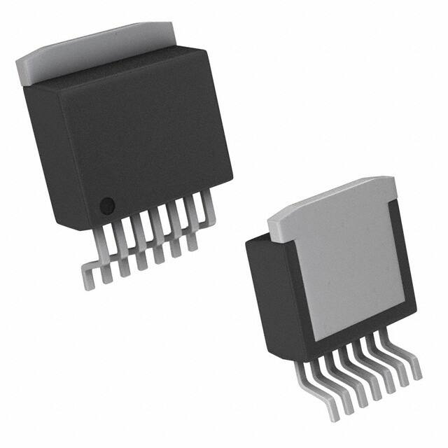
D2PAK−7
DPS SUFFIX
CASE 936AB
Pin 1. VSTBY
2. VIN
3. VTRK
4. GND
5. Adj
6. ENABLE
7. RESET
MARKING DIAGRAM
Features
CS8363
AWLYWW
• 2 Regulated Outputs
− Standby Output 3.3 V −2%, +2.4%; 100 mA
− Adjustable Tracking Output; 250 mA
• Operation down to VIN = 4.5 V
• RESET for VSTBY
• ENABLE for VTRK
• Low Quiescent Current
• Protection Features
− Independent Thermal Shutdown
− Short Circuit
− 60 V Load Dump
− Reverse Battery
1
A
WL
Y
WW
= Assembly Location
= Wafer Lot
= Year
= Work Week
ORDERING INFORMATION*
Package
Shipping†
CS8363YDPS7
D2PAK−7
50 Units/Rail
CS8363YDPSR7
D2PAK−7
750 Tape & Reel
Device
†For information on tape and reel specifications,
including part orientation and tape sizes, please
refer to our Tape and Reel Packaging Specifications
Brochure, BRD8011/D.
© Semiconductor Components Industries, LLC, 2009
October, 2009 − Rev. 12
1
Publication Order Number:
CS8363/D
�CS8363
VSTBY
3.3 V, 100 mA, 2.0%
VIN
Overvoltage
Shutdown
Current
Limit
Bandgap
RESET
BG
+
OVSD
BG
−
TSD OVSD
VIN
VTRK
250 mA
Current
Limit
Thermal
Shutdown
TSD
−
Adj
+
ENABLE
VSTBY
−
+
TSD OVSD
BG
RESET
+
GND
−
RESET
Figure 1. Block Diagram. Consult Your Local Sales Representative for Positive ENABLE Option
ABSOLUTE MAXIMUM RATINGS*
Rating
Value
Unit
−16 to 26
V
Positive Transient Input Voltage, tr > 1.0 ms
60
V
Negative Transient Input Voltage, T < 100 ms, 1.0 % Duty Cycle
−50
V
−0.3 to 10
V
Junction Temperature
−40 to +150
°C
Storage Temperature Range
−55 to +150
°C
2.0
kV
260 peak
230 peak
°C
°C
Supply Voltage, VIN
Input Voltage Range (ENABLE, RESET)
ESD Susceptibility (Human Body Model)
Lead Temperature Soldering
Wave Solder (through hole styles only) Note 1
Reflow (SMD styles only) Note 2
Stresses exceeding Maximum Ratings may damage the device. Maximum Ratings are stress ratings only. Functional operation above the
Recommended Operating Conditions is not implied. Extended exposure to stresses above the Recommended Operating Conditions may affect
device reliability.
1. 10 seconds max.
2. 60 seconds max above 183°C
*The maximum package power dissipation must be observed.
http://onsemi.com
2
�CS8363
ELECTRICAL CHARACTERISTICS (6.0 V ≤ VIN ≤ 26 V, IOUT1 = IOUT2 = 100 mA, −40°C ≤ TA ≤ +125°C;
unless otherwise stated.)
Test Conditions
Characteristic
Min
Typ
Max
Unit
−25
−
+25
mV
Tracking Output (VTRK)
VTRK Tracking Error (VSTBY − VTRK)
6.0 V ≤ VIN ≤ 26 V, 100 mA ≤ ITRK ≤ 250 mA.
Note 3
Adjust Pin Current, IAdj
Loop in Regulation
−
1.5
5.0
mA
Line Regulation
6.0 V ≤ VIN ≤ 26 V. Note 3
−
5.0
50
mV
Load Regulation
100 mA ≤ ITRK ≤ 250 mA. Note 3
−
5.0
50
mV
Dropout Voltage (VIN − VTRK)
ITRK = 100 mA.
ITRK = 250 mA
−
−
−
−
1.05
1.05
mV
mV
Current Limit
VIN = 12 V, VTRK = 3.0 V
275
500
−
mA
Quiescent Current
VIN = 12 V, ITRK = 250 mA, No Load on VSTBY
VIN = 12 V, ITRK = 500 mA, ISTBY = 100 mA
−
−
25
145
50
220
mA
mA
Reverse Current
VTRK = 3.3 V, VIN = 0 V
−
200
1500
mA
Ripple Rejection
f = 120 Hz, ITRK = 250 mA, 7.0 V ≤ VIN ≤ 17 V
60
70
−
dB
Output Voltage, VSTBY
4.5 V ≤ VIN ≤ 26 V, 100 mA ≤ ISTBY ≤ 100 mA.
3.234
3.3
3.380
V
Line Regulation
6.0 V ≤ VIN ≤ 26 V.
−
5.0
50
mV
Load Regulation
100 mA ≤ ISTBY ≤ 100 mA.
−
5.0
50
mV
Dropout Voltage (VIN − VSTBY)
ISTBY = 100 mA, VIN = 4.2 V
ISTBY = 100 mA, VIN = 4.2 V
−
−
−
−
1.05
1.05
V
V
Current Limit
VIN = 12 V, VSTBY = 3.0 V
125
200
−
mA
Short Circuit Current
VIN = 12 V, VSTBY = 0 V
10
100
−
mA
Quiescent Current
VIN = 12 V, ISTBY = 100 mA, ITRK = 0 mA
VIN = 12 V, ISTBY = 300 mA, ITRK = 0 mA
−
−
10
140
20
200
mA
mA
Reverse Current
VSTBY = 3.3 V, VIN = 0 V
−
100
200
mA
Ripple Rejection
f = 120 Hz, ISTBY = 100 mA, 7.0 V ≤ VIN ≤ 17 V
60
70
−
dB
−
0.8
1.2
2.0
V
−10
0
10
mA
10
50
150
mV
92.5
95
97.5
%VSTBY
−
−
25
mA
Standby Output (VSTBY)
RESET ENABLE Functions
ENABLE Input Threshold
ENABLE Input Bias Current
VENABLE = 0 V to 10 V
RESET Hysteresis
RESET Threshold Low (VRL)
−
VSTBY Decreasing, VIN > 4.5 V
RESET Leakage
−
Output Voltage, Low (VRLO)
1.0 V ≤ VSTBY ≤ VRL, RRST = 10 kW
−
0.1
0.4
V
Output Voltage, Low (VRPEAK)
VSTBY, Power Up, Power Down
−
0.6
1.0
V
VIN (VRST Low)
VSTBY = 3.3 V
−
4.0
4.5
V
150
150
180
165
−
−
°C
°C
30
34
38
V
Protection Circuitry (Both Outputs)
Independent Thermal Shutdown
Overvoltage Shutdown
VSTBY
VTRK
−
3. VTRK connected to Adj lead. VTRK can be set to higher values by using an external resistor divider.
http://onsemi.com
3
�CS8363
PACKAGE PIN DESCRIPTION
PACKAGE PIN #
D2PAK−7
PIN SYMBOL
1
VSTBY
2
VIN
3
VTRK
Tracking output voltage controlled by ENABLE delivering 250 mA.
4
GND
Reference ground connection.
5
Adj
6
ENABLE
7
RESET
FUNCTION
Standby output voltage delivering 100 mA.
Input voltage.
Resistor divider from VTRK to Adj. Sets the output voltage on VTRK. If tied to
VTRK, VTRK will track VSTBY.
Provides on/off control of the tracking output, active LOW.
CMOS compatible output lead that goes low whenever VSTBY falls out of
regulation.
CIRCUIT DESCRIPTION
ENABLE Function
VTRK Output Voltage
The ENABLE function switches the output transistor for
VTRK on and off. When the ENABLE lead voltage exceeds
1.4 V (Typ), VTRK turns off. This input has several hundred
millivolts of hysteresis to prevent spurious output activity
during power−up or power−down.
This output uses the same type of output device as VSTBY,
but is rated for 250 mA. The output is configured as a
tracking regulator of the standby output. By using the
standby output as a voltage reference, giving the user an
external programming lead (Adj lead), output voltages from
3.3 V to 20 V are easily realized. The programming is done
with a simple resistor divider, and following the formula:
RESET Function
The RESET is an open collector NPN transistor,
controlled by a low voltage detection circuit sensing the
VSTBY (3.3 V) output voltage. This circuit guarantees the
RESET output stays below 1.0 V (0.1 V Typ) when VSTBY
is as low as 1.0 V to ensure reliable operation of
microprocessor−based systems.
B+
C1*
0.1 mF
VTRK + VSTBY
CS8363
3.3 V, 100 mA
C2**
10 mF
ESR < 8.0 W
R3
RESET
VDD
MCU
RESET
I/O
ENABLE
R2
Adj
R1
GND
R1
If another 3.3 V output is needed, simply connect the Adj
lead to the VTRK output lead.
VSTBY
VIN
(1 ) R1ńR2) ) IAdj
VTRK
SW 5.0 V,
250 mA
C3**
10 mF
ESR < 8.0 W
VTRK ∼ VSTBY(1 + R1/R2)
For VTRK ∼ 5.0 V, R1/R2 ∼ 0.5
*C1 is required if regulator is located far from power supply filter.
**C2 and C3 are required for stability.
Figure 2. Test and Application Circuit, 3.3 V, 5.0 V Regulator
http://onsemi.com
4
GND
�CS8363
B+
C1*
0.1 mF
3.3 V, 100 mA
VSTBY
VIN
CS8363
VDD
C2**
10 mF
ESR < 8.0 W
R3
RESET
MCU
RESET
I/O
ENABLE
Adj
GND
SW 3.3 V,
250 mA
C3**
10 mF
ESR < 8.0 W
VTRK
GND
*C1 is required if regulator is located far from power supply filter.
**C2 and C3 are required for stability.
Figure 3. Test and Application Circuit, Dual 3.3 V Regulator
APPLICATION NOTES
External Capacitors
IOUT1(max) is the maximum output current, for the
application,
IOUT2(max) is the maximum output current, for the
application, and
IQ is the quiescent current the regulator consumes at both
IOUT1(max) and IOUT2(max).
Once the value of PD(max) is known, the maximum
permissible value of RqJA can be calculated:
Output capacitors for the CS8363 are required for
stability. Without them, the regulator outputs will oscillate.
Actual size and type may vary depending upon the
application load and temperature range. Capacitor effective
series resistance (ESR) is also a factor in the IC stability.
Worst−case is determined at the minimum ambient
temperature and maximum load expected.
Output capacitors can be increased in size to any desired
value above the minimum. One possible purpose of this
would be to maintain the output voltages during brief
conditions of negative input transients that might be
characteristic of a particular system.
Capacitors must also be rated at all ambient temperatures
expected in the system. To maintain regulator stability down
to −40°C, capacitors rated at that temperature must be used.
More information on capacitor selection for SMART
REGULATOR®s is available in the SMART REGULATOR
application note, “Compensation for Linear Regulators,”
document number SR003AN/D, available through the
Literature Distribution Center or via our website at
http://www.onsemi.com.
RQJA +
150° C * TA
PD
(2)
The value of RqJA can be compared with those in the
package section of the data sheet. Those packages with
RqJA’s less than the calculated value in equation 2 will keep
the die temperature below 150°C.
In some cases, none of the packages will be sufficient to
dissipate the heat generated by the IC, and an external
heatsink will be required.
VIN
Calculating Power Dissipation in a
Dual Output Linear Regulator
IIN
SMART
REGULATOR
Control
Features
The maximum power dissipation for a dual output
regulator (Figure 4) is
PD(max) + NJVIN(max) * VOUT1(min)NjIOUT1(max) )
NJVIN(max) * VOUT2(min)NjIOUT2(max) ) VIN(max)IQ (1)
IOUT1
IOUT2
VOUT1
VOUT2
IQ
where:
VIN(max) is the maximum input voltage,
VOUT1(min) is the minimum output voltage from VOUT1,
VOUT2(min) is the minimum output voltage from VOUT2,
Figure 4. Dual Output Regulator With Key
Performance Parameters Labeled.
http://onsemi.com
5
�CS8363
Heat Sinks
where:
RqJC = the junction−to−case thermal resistance,
RqCS = the case−to−heatsink thermal resistance, and
RqSA = the heatsink−to−ambient thermal resistance.
A heat sink effectively increases the surface area of the
package to improve the flow of heat away from the IC and
into the surrounding air.
Each material in the heat flow path between the IC and the
outside environment will have a thermal resistance. Like
series electrical resistances, these resistances are summed to
determine the value of RqJA:
RQJA + RQJC ) RQCS ) RQSA
RqJC appears in the package section of the data sheet. Like
RqJA, it too is a function of package type. RqCS and RqSA are
functions of the package type, heatsink and the interface
between them. These values appear in heat sink data sheets
of heat sink manufacturers.
(3)
SMART REGULATOR is a registered trademark of Semiconductor Components Industries, LLC (SCILLC).
http://onsemi.com
6
�MECHANICAL CASE OUTLINE
PACKAGE DIMENSIONS
D2PAK−7 (SHORT LEAD)
CASE 936AB−01
ISSUE B
DATE 08 SEP 2009
A
1
SCALE 1:1
E
L1
B
A
0.10
A
E/2
NOTES:
1. DIMENSIONING AND TOLERANCING PER ASME
Y14.5M, 1994.
2. CONTROLLING DIMENSION: INCHES.
3. DIMENSIONS D AND E DO NOT INCLUDE MOLD
FLASH AND GATE PROTRUSIONS. MOLD FLASH
AND GATE PROTRUSIONS NOT TO EXCEED
0.005 MAXIMUM PER SIDE. THESE DIMENSIONS
TO BE MEASURED AT DATUM H.
4. THERMAL PAD CONTOUR OPTIONAL WITHIN
DIMENSIONS E, L1, D1, AND E1. DIMENSIONS
D1 AND E1 ESTABLISH A MINIMUM MOUNTING
SURFACE FOR THE THERMAL PAD.
SEATING
PLANE
M
B A
M
E1
c2
D1
D
7X
H
DETAIL C
e
b
0.13
M
B A
VIEW A−A
c
A
M
B
H
SEATING
PLANE
A1
RECOMMENDED
SOLDERING FOOTPRINT*
L
0.424
INCHES
MIN
MAX
0.170
0.180
0.000
0.010
0.026
0.036
0.017
0.026
0.045
0.055
0.325
0.368
0.270
−−−
0.380
0.420
0.245
−−−
0.050 BSC
0.539
0.579
0.058
0.078
−−−
0.066
0.010 BSC
0°
8°
MILLIMETERS
MIN
MAX
4.32
4.57
0.00
0.25
0.66
0.91
0.43
0.66
1.14
1.40
8.25
9.53
6.86
−−−
9.65
10.67
6.22
−−−
1.27 BSC
13.69
14.71
1.47
1.98
−−−
1.68
0.25 BSC
0°
8°
GENERIC
MARKING DIAGRAM*
M
L3
DIM
A
A1
b
c
c2
D
D1
E
E1
e
H
L
L1
L3
M
GAUGE
PLANE
XX
XXXXXXXXX
AWLYWWG
DETAIL C
0.310
0.584
1
XXXXX
A
WL
Y
WW
G
0.136
7X
0.050
PITCH
0.040
DIMENSIONS: MILLIMETERS
*For additional information on our Pb−Free strategy and soldering
details, please download the ON Semiconductor Soldering and
Mounting Techniques Reference Manual, SOLDERRM/D.
DOCUMENT NUMBER:
DESCRIPTION:
98AON14119D
D2PAK−7 (SHORT LEAD)
= Specific Device Code
= Assembly Location
= Wafer Lot
= Year
= Work Week
= Pb−Free Package
*This information is generic. Please refer to
device data sheet for actual part marking.
Pb−Free indicator, “G” or microdot “ G”,
may or may not be present.
Electronic versions are uncontrolled except when accessed directly from the Document Repository.
Printed versions are uncontrolled except when stamped “CONTROLLED COPY” in red.
PAGE 1 OF 1
ON Semiconductor and
are trademarks of Semiconductor Components Industries, LLC dba ON Semiconductor or its subsidiaries in the United States and/or other countries.
ON Semiconductor reserves the right to make changes without further notice to any products herein. ON Semiconductor makes no warranty, representation or guarantee regarding
the suitability of its products for any particular purpose, nor does ON Semiconductor assume any liability arising out of the application or use of any product or circuit, and specifically
disclaims any and all liability, including without limitation special, consequential or incidental damages. ON Semiconductor does not convey any license under its patent rights nor the
rights of others.
© Semiconductor Components Industries, LLC, 2019
www.onsemi.com
�onsemi,
, and other names, marks, and brands are registered and/or common law trademarks of Semiconductor Components Industries, LLC dba “onsemi” or its affiliates
and/or subsidiaries in the United States and/or other countries. onsemi owns the rights to a number of patents, trademarks, copyrights, trade secrets, and other intellectual property.
A listing of onsemi’s product/patent coverage may be accessed at www.onsemi.com/site/pdf/Patent−Marking.pdf. onsemi reserves the right to make changes at any time to any
products or information herein, without notice. The information herein is provided “as−is” and onsemi makes no warranty, representation or guarantee regarding the accuracy of the
information, product features, availability, functionality, or suitability of its products for any particular purpose, nor does onsemi assume any liability arising out of the application or use
of any product or circuit, and specifically disclaims any and all liability, including without limitation special, consequential or incidental damages. Buyer is responsible for its products
and applications using onsemi products, including compliance with all laws, regulations and safety requirements or standards, regardless of any support or applications information
provided by onsemi. “Typical” parameters which may be provided in onsemi data sheets and/or specifications can and do vary in different applications and actual performance may
vary over time. All operating parameters, including “Typicals” must be validated for each customer application by customer’s technical experts. onsemi does not convey any license
under any of its intellectual property rights nor the rights of others. onsemi products are not designed, intended, or authorized for use as a critical component in life support systems
or any FDA Class 3 medical devices or medical devices with a same or similar classification in a foreign jurisdiction or any devices intended for implantation in the human body. Should
Buyer purchase or use onsemi products for any such unintended or unauthorized application, Buyer shall indemnify and hold onsemi and its officers, employees, subsidiaries, affiliates,
and distributors harmless against all claims, costs, damages, and expenses, and reasonable attorney fees arising out of, directly or indirectly, any claim of personal injury or death
associated with such unintended or unauthorized use, even if such claim alleges that onsemi was negligent regarding the design or manufacture of the part. onsemi is an Equal
Opportunity/Affirmative Action Employer. This literature is subject to all applicable copyright laws and is not for resale in any manner.
PUBLICATION ORDERING INFORMATION
LITERATURE FULFILLMENT:
Email Requests to: orderlit@onsemi.com
onsemi Website: www.onsemi.com
◊
TECHNICAL SUPPORT
North American Technical Support:
Voice Mail: 1 800−282−9855 Toll Free USA/Canada
Phone: 011 421 33 790 2910
Europe, Middle East and Africa Technical Support:
Phone: 00421 33 790 2910
For additional information, please contact your local Sales Representative
�


 工商网监
湘ICP备2023018690号
工商网监
湘ICP备2023018690号
