ON Semiconductor
Is Now
To learn more about onsemi™, please visit our website at
www.onsemi.com
onsemi and and other names, marks, and brands are registered and/or common law trademarks of Semiconductor Components Industries, LLC dba “onsemi” or its affiliates and/or
subsidiaries in the United States and/or other countries. onsemi owns the rights to a number of patents, trademarks, copyrights, trade secrets, and other intellectual property. A listing of onsemi
product/patent coverage may be accessed at www.onsemi.com/site/pdf/Patent-Marking.pdf. onsemi reserves the right to make changes at any time to any products or information herein, without
notice. The information herein is provided “as-is” and onsemi makes no warranty, representation or guarantee regarding the accuracy of the information, product features, availability, functionality,
or suitability of its products for any particular purpose, nor does onsemi assume any liability arising out of the application or use of any product or circuit, and specifically disclaims any and all
liability, including without limitation special, consequential or incidental damages. Buyer is responsible for its products and applications using onsemi products, including compliance with all laws,
regulations and safety requirements or standards, regardless of any support or applications information provided by onsemi. “Typical” parameters which may be provided in onsemi data sheets and/
or specifications can and do vary in different applications and actual performance may vary over time. All operating parameters, including “Typicals” must be validated for each customer application
by customer’s technical experts. onsemi does not convey any license under any of its intellectual property rights nor the rights of others. onsemi products are not designed, intended, or authorized
for use as a critical component in life support systems or any FDA Class 3 medical devices or medical devices with a same or similar classification in a foreign jurisdiction or any devices intended for
implantation in the human body. Should Buyer purchase or use onsemi products for any such unintended or unauthorized application, Buyer shall indemnify and hold onsemi and its officers, employees,
subsidiaries, affiliates, and distributors harmless against all claims, costs, damages, and expenses, and reasonable attorney fees arising out of, directly or indirectly, any claim of personal injury or death
associated with such unintended or unauthorized use, even if such claim alleges that onsemi was negligent regarding the design or manufacture of the part. onsemi is an Equal Opportunity/Affirmative
Action Employer. This literature is subject to all applicable copyright laws and is not for resale in any manner. Other names and brands may be claimed as the property of others.
�EcoSPARK®2 335mJ, 400V, N-Channel Ignition IGBT
Features
Applications
o
SCIS Energy = 335mJ at TJ = 25 C
Automotive lgnition Coil Driver Circuits
Logic Level Gate Drive
Coil On Plug Applications
Qualified to AEC Q101
RoHS Compliant
Package
Symbol
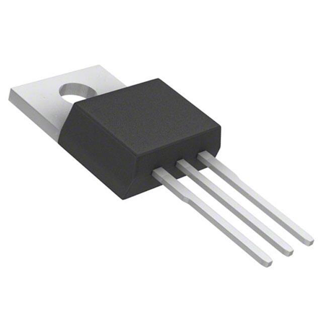
JEDEC TO-263AB
D²-Pak
JEDEC TO-220AB
E
C
G
COLLECTOR
G
E
R1
GATE
JEDEC TO-252AA
D-Pak
R2
G
E
EMITTER
COLLECTOR
(FLANGE)
Device Maximum Ratings TA = 25°C unless otherwise noted
Symbol
Parameter
BVCER Collector to Emitter Breakdown Voltage (IC = 1mA)
Ratings
400
Units
V
BVECS
Emitter to Collector Voltage - Reverse Battery Condition (IC = 10mA)
28
V
ESCIS25
Self Clamping Inductive Switching Energy (Note 1)
335
mJ
195
mJ
ESCIS150 Self Clamping Inductive Switching Energy (Note 2)
IC25
Collector Current Continuous, at VGE = 4.0V, TC = 25°C
26.9
A
IC110
Collector Current Continuous, at VGE = 4.0V, TC = 110°C
25
A
VGEM
Gate to Emitter Voltage Continuous
±10
V
Power Dissipation Total, at TC = 25°C
166
W
1.1
W/oC
PD
Power Dissipation Derating, for TC > 25oC
TJ
Operating Junction Temperature Range
-40 to +175
o
C
TSTG
Storage Junction Temperature Range
-40 to +175
o
C
TL
Max. Lead Temp. for Soldering (Leads at 1.6mm from case for 10s)
300
o
C
TPKG
Max. Lead Temp. for Soldering (Package Body for 10s)
260
o
C
ESD
Electrostatic Discharge Voltage at100pF, 1500Ω
@2014 Semiconductor Components Industries, LLC.
August-2017, Rev.3
4
kV
Publication Order Number:
FGB3440G2-F085/D
FGB3440G2-F085 / FGD3440G2-F085 / FGP3440G2-F085
FGB3440G2-F085 / FGD3440G2-F085
FGP3440G2-F085
�Device
Device Marking
Package
FGB3440G2
FGB3440G2-F085
FGD3440G2
FGD3440G2-F085
TO-263AB
TO-252AA
FGP3440G2
FGP3440G2-F085
TO-220AB
Reel Size
330mm
Tape Width
24mm
800
330mm
16mm
N/A
2500
50
Tube
Quantity
Electrical Characteristics TA = 25°C unless otherwise noted
Symbol
Parameter
Test Conditions
Min
Typ
Max Units
Off State Characteristics
BVCER
ICE = 2mA, VGE = 0,
Collector to Emitter Breakdown Voltage RGE = 1KΩ,
TJ = -40 to 150oC
370
400
430
V
BVCES
ICE = 10mA, VGE = 0V,
Collector to Emitter Breakdown Voltage RGE = 0,
TJ = -40 to 150oC
390
420
450
V
BVECS
Emitter to Collector Breakdown Voltage
ICE = -20mA, VGE = 0V,
TJ = 25°C
28
-
-
V
BVGES
Gate to Emitter Breakdown Voltage
IGES = ±2mA
±12
±14
-
V
Collector to Emitter Leakage Current
VCE = 250V, RGE=1KΩ
-
-
25
μA
-
-
1
mA
IECS
Emitter to Collector Leakage Current
VEC = 24V,
-
-
1
-
-
40
R1
Series Gate Resistance
R2
Gate to Emitter Resistance
ICER
TJ = 25oC
TJ = 150oC
TJ = 25oC
TJ = 150oC
mA
-
120
-
Ω
10K
-
30K
Ω
-
1.1
1.2
V
-
1.3
1.45
V
-
1.6
1.75
V
-
-
335
mJ
On State Characteristics
VCE(SAT) Collector to Emitter Saturation Voltage ICE = 6A, VGE = 4V,
VCE(SAT) Collector to Emitter Saturation Voltage ICE = 10A, VGE = 4.5V,
VCE(SAT) Collector to Emitter Saturation Voltage ICE = 15A, VGE = 4.5V,
L = 3.0 mHy, VGE = 5V
ESCIS
Self Clamped Inductive Switching
RG = 1KΩ, (Note 1)
TJ = 25oC
TJ = 150oC
TJ = 150oC
o
TJ = 25 C
Notes:
1: Self Clamping Inductive Switching Energy(ESCIS25) of 335mJ is based on the test conditions that is starting
TJ=25 oC; L=3mHy, ISCIS=15A,VCC=100V during inductor charging and VCC=0V during the time in clamp .
2: Self Clamping Inductive Switching Energy (ESCIS150) of 195mJ is based on the test conditions that is starting
TJ=150 oC; L=3mHy, ISCIS=11.4A,VCC=100V during inductor charging and VCC=0V during the time in clamp.
www.onsemi.com
2
FFGB3440G2-F085 / FGD3440G2-F085 / FGP3440G2-F085
Package Marking and Ordering Information
�Symbol
Parameter
Test Conditions
Min
Typ
-
24
Max Units
Dynamic Characteristics
QG(ON)
Gate Charge
ICE = 10A, VCE = 12V,
VGE = 5V
-
nC
1.3
1.7
2.2
0.75
1.2
1.8
VCE = 12V, ICE = 10A
-
2.8
-
V
Current Turn-On Delay Time-Resistive VCE = 14V, RL = 1Ω
VGE = 5V, RG = 1KΩ
Current Rise Time-Resistive
TJ = 25oC,
-
1.0
4
μs
-
2.0
7
μs
-
5.3
15
μs
-
2.3
15
μs
-
-
0.9
oC/W
VGE(TH)
Gate to Emitter Threshold Voltage
ICE = 1mA, VCE = VGE,
VGEP
Gate to Emitter Plateau Voltage
TJ =
25oC
TJ = 150oC
V
Switching Characteristics
td(ON)R
trR
td(OFF)L
tfL
Current Turn-Off Delay Time-Inductive VCE = 300V, L = 1mH,
VGE = 5V, RG = 1KΩ
Current Fall Time-Inductive
ICE =6.5A, TJ = 25oC,
Thermal Characteristics
RθJC
Thermal Resistance Junction to Case
www.onsemi.com
3
FGB3440G2-F085 / FGD3440G2-F085 / FGP3440G2-F085
Electrical Characteristics TA = 25°C unless otherwise noted
�10
o
TJ = 150 C
1
10
SCIS Curves valid for Vclamp Voltages of


 工商网监
湘ICP备2023018690号
工商网监
湘ICP备2023018690号
