MC10EP131, MC100EP131
3.3V / 5V�ECL Quad D
Flip−Flop with Set, Reset,
and Differential Clock
Description
The MC10/100EP131 is a Quad Master−slaved D flip−flop with
common set and separate resets. The device is an expansion of the
E131 with differential common clock and individual clock enables.
With AC performance faster than the E131 device, the EP131 is ideal
for applications requiring the fastest AC performance available.
Each flip−flop may be clocked separately by holding Common
Clock (CC) LOW and CC HIGH, then using the differential Clock
Enable inputs for clocking (C0−3, C0−3).
Common clocking is achieved by holding the differential inputs
C0−3 LOW and C0−3 HIGH while using the differential Common
Clock (CC) to clock all four flip−flops. When left floating open, any
differential input will disable operation due to input pulldown resistors
forcing an output default state.
Individual asynchronous resets (R0−3) and an asynchronous set
(SET) are provided.
Data enters the master when both CC and C0−3 are LOW, and
transfers to the slave when either CC or C0−3 (or both) go HIGH.
The 100 Series contains temperature compensation.
Features
•
•
•
•
•
•
•
•
•
•
•
November, 2006 − Rev. 10
MARKING
DIAGRAM*
MCxxx
EP131
AWLYYWWG
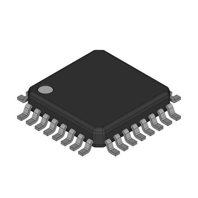
LQFP−32
FA SUFFIX
CASE 873A
1
1
32
QFN32
MN SUFFIX
CASE 488AM
xxx
A
WL, L
YY, Y
WW, W
G or G
460 ps Typical Propagation Delay
Maximum Frequency > 3 GHz Typical
Differential Individual and Common Clocks
Individual Asynchronous Resets
Asynchronous Set
PECL Mode Operating Range: VCC = 3.0 V to 5.5 V
with VEE = 0 V
NECL Mode Operating Range: VCC = 0 V
with VEE = −3.0 V to −5.5 V
Open Input Default State
Safety Clamp on Inputs
Q Output Will Default LOW with Inputs Open or at VEE
Pb−Free Packages are Available
© Semiconductor Components Industries, LLC, 2006
http://onsemi.com
MCxxx
EP131
AWLYYWWG
G
= 10 or 100
= Assembly Location
= Wafer Lot
= Year
= Work Week
= Pb−Free Package
(Note: Microdot may be in either location)
*For additional marking information, refer to
Application Note AND8002/D.
ORDERING INFORMATION
See detailed ordering and shipping information in the package
dimensions section on page 9 of this data sheet.
1
Publication Order Number:
MC10EP131/D
�MC10EP131, MC100EP131
Q3 Q3 Q2
Q2 Q1 Q1
Q0 Q0
D2 SET R3
32
24
23
22
21
20
19
18
17
31
30
D3 VEE C3
29
28
C3 VCC
27
26
25
R2
1
24 Q3
VCC
25
16
VCC
C2
2
23 Q3
C3
26
15
R0
C2
3
22 Q2
C3
27
14
D0
CC
4
VEE
28
13
VCC
CC
5
D3
29
12
C0
C1
6
19 Q1
R3
30
11
C0
C1
7
18 Q0
SET
31
10
R1
D1
8
17 Q0
D2
32
9
VEE
32−Lead LQFP Pinout
(Top View)
1
2
3
4
5
6
7
9
8
21 Q2
MC10EP131
MC100EP131
10
11
12
13
VEE R1
C0
C0 VCC D0
20 Q1
14
15
16
R0 VCC
Figure 2. 32−Lead QFN Pinout (Top View)
R2
C2 C2
CC CC C1
C1
D1
Warning: All VCC and VEE pins must be externally connected
to Power Supply to guarantee proper operation.
D3
Figure 1. 32−Lead LQFP Pinout (Top View)
C3
D
C3
Table 1. PIN DESCRIPTION
PIN
FUNCTION
ECL Data Inputs
C0−3*, C0−3*
ECL Separate Clock Inputs
CC*, CC*
ECL Common Clock Inputs
R0−3*
ECL Asynchronous Reset
SET*
ECL Asynchronous Set
Q0−3, Q0−3
ECL Data Outputs
VCC
Positive Supply
VEE
Negative Supply
EP for
QFN−32, only
The Exposed Pad (EP) on the
QFN−32 package bottom is
thermally connected to the die
for improved heat transfer out
of package. The exposed pad
must be attached to a heat−
sinking conduit. The pad is
electrically connected to VEE.
D2
L
H
X
X
X
L
L
H
L
H
L
L
L
H
H
D
C2
Q
Q3
S
Q
Q2
R
Q
Q2
Q
Q1
Q
Q1
Q
Q0
Q
Q0
R2
SET
CC
CC
R1
R
C1
C1
D1
D
S
R0
Table 2. TRUTH TABLE
R*
Q3
C2
* Pins will default LOW when left open.
S*
R
Q
R3
D0−3*
D
S
CLK
Z
Z
X
X
X
R
C0
Q
C0
L
H
H
L
Undef
D0
D
S
VEE
Z = LOW to HIGH Transition
Figure 3. Logic Diagram
* Pins will default low when left open.
http://onsemi.com
2
�MC10EP131, MC100EP131
Table 3. ATTRIBUTES
Characteristics
Value
Internal Input Pulldown Resistor
75 kW
Internal Input Pullup Resistor
N/A
ESD Protection
Human Body Model
Machine Model
Charged Device Model
> 2 kV
> 100 V
> 2 kV
Moisture Sensitivity, Indefinite Time Out of Drypack (Note 1)
LQFP−32
QFN−32
Flammability Rating
Pb Pkg
Pb−Free Pkg
Level 2
Level 2
Level 1
Oxygen Index: 28 to 34
UL 94 V−0 @ 0.125 in
Transistor Count
935 Devices
Meets or exceeds JEDEC Spec EIA/JESD78 IC Latchup Test
1. For additional information, see Application Note AND8003/D.
Table 4. MAXIMUM RATINGS
Symbol
Parameter
Condition 1
Condition 2
Rating
Unit
VCC
PECL Mode Power Supply
VEE = 0 V
6
V
VEE
NECL Mode Power Supply
VCC = 0 V
−6
V
VI
PECL Mode Input Voltage
NECL Mode Input Voltage
VEE = 0 V
VCC = 0 V
6
−6
V
V
Iout
Output Current
Continuous
Surge
50
100
mA
mA
IBB
VBB Sink/Source
± 0.5
mA
TA
Operating Temperature Range
−40 to +85
°C
Tstg
Storage Temperature Range
−65 to +150
°C
qJA
Thermal Resistance (Junction−to−Ambient)
0 lfpm
500 lfpm
32 LQFP
32 LQFP
80
55
°C/W
°C/W
qJC
Thermal Resistance (Junction−to−Case)
Standard Board
32 LQFP
12 to 17
°C/W
qJA
Thermal Resistance (Junction−to−Ambient)
0 lfpm
500 lfpm
QFN−32
QFN−32
31
27
°C/W
°C/W
qJC
Thermal Resistance (Junction−to−Case)
2S2P
QFN−32
12
°C/W
Tsol
Wave Solder
265
265
°C
Pb
Pb−Free
VI ≤ VCC
VI ≥ VEE
Stresses exceeding Maximum Ratings may damage the device. Maximum Ratings are stress ratings only. Functional operation above the
Recommended Operating Conditions is not implied. Extended exposure to stresses above the Recommended Operating Conditions may affect
device reliability.
http://onsemi.com
3
�MC10EP131, MC100EP131
Table 5. 10EP DC CHARACTERISTICS, PECL VCC = 3.3 V, VEE = 0 V (Note 2)
−40°C
Symbol
Characteristic
25°C
85°C
Min
Typ
Max
Min
Typ
Max
Min
Typ
Max
Unit
70
95
120
70
95
120
70
95
120
mA
IEE
Power Supply Current
VOH
Output HIGH Voltage (Note 3)
2165
2290
2415
2230
2355
2480
2290
2415
2540
mV
VOL
Output LOW Voltage (Note 3)
1365
1490
1615
1430
1555
1680
1490
1615
1740
mV
VIH
Input HIGH Voltage (Single−Ended)
2090
2415
2155
2480
2215
2540
mV
VIL
Input LOW Voltage (Single−Ended)
1365
1690
1460
1755
1490
1815
mV
VIHCMR
Input HIGH Voltage Common Mode
Range (Differential Configuration)
(Note 4)
2.0
3.3
2.0
3.3
2.0
3.3
V
IIH
Input HIGH Current
150
mA
IIL
Input LOW Current
150
0.5
150
0.5
0.5
mA
NOTE: Device will meet the specifications after thermal equilibrium has been established when mounted in a test socket or printed circuit
board with maintained transverse airflow greater than 500 lfpm. Electrical parameters are guaranteed only over the declared
operating temperature range. Functional operation of the device exceeding these conditions is not implied. Device specification limit
values are applied individually under normal operating conditions and not valid simultaneously.
2. Input and output parameters vary 1:1 with VCC. VEE can vary +0.3 V to −2.2 V.
3. All loading with 50 W to VCC − 2.0 V.
4. VIHCMR min varies 1:1 with VEE, VIHCMR max varies 1:1 with VCC. The VIHCMR range is referenced to the most positive side of the differential
input signal.
Table 6. 10EP DC CHARACTERISTICS, PECL VCC = 5.0 V, VEE = 0 V (Note 5)
−40°C
Symbol
Characteristic
Min
Typ
25°C
Max
Min
Typ
85°C
Max
Min
Typ
Max
Unit
IEE
Power Supply Current
70
95
120
70
95
120
70
95
120
mA
VOH
Output HIGH Voltage (Note 6)
3865
3990
4115
3930
4055
4180
3990
4115
4240
mV
VOL
Output LOW Voltage (Note 6)
3065
3190
3315
3130
3255
3380
3190
3315
3440
mV
VIH
Input HIGH Voltage (Single−Ended)
3790
4115
3855
4180
3915
4240
mV
VIL
Input LOW Voltage (Single−Ended)
3065
3390
3130
3455
3190
3515
mV
VIHCMR
Input HIGH Voltage Common Mode
Range (Differential Configuration)
(Note 7)
2.0
5.0
2.0
5.0
2.0
5.0
V
IIH
Input HIGH Current
150
mA
IIL
Input LOW Current
150
0.5
150
0.5
0.5
mA
NOTE: Device will meet the specifications after thermal equilibrium has been established when mounted in a test socket or printed circuit
board with maintained transverse airflow greater than 500 lfpm. Electrical parameters are guaranteed only over the declared
operating temperature range. Functional operation of the device exceeding these conditions is not implied. Device specification limit
values are applied individually under normal operating conditions and not valid simultaneously.
5. Input and output parameters vary 1:1 with VCC. VEE can vary +2.0 V to −0.5 V.
6. All loading with 50 W to VCC − 2.0 V.
7. VIHCMR min varies 1:1 with VEE, VIHCMR max varies 1:1 with VCC. The VIHCMR range is referenced to the most positive side of the differential
input signal.
http://onsemi.com
4
�MC10EP131, MC100EP131
Table 7. 10EP DC CHARACTERISTICS, NECL VCC = 0 V, VEE = −5.5 V to −3.0 V (Note 8)
−40°C
Symbol
Characteristic
25°C
85°C
Min
Typ
Max
Min
Typ
Max
Min
Typ
Max
Unit
70
95
120
70
95
120
70
95
120
mA
IEE
Power Supply Current
VOH
Output HIGH Voltage (Note 9)
−1135
−1010
−885
−1070
−945
−820
−1010
−885
−760
mV
VOL
Output LOW Voltage (Note 9)
−1935
−1810
−1685
−1870
−1745
−1620
−1810
−1685
−1560
mV
VIH
Input HIGH Voltage (Single−Ended)
−1210
−885
−1145
−820
−1085
−760
mV
VIL
Input LOW Voltage (Single−Ended)
−1935
−1610
−1870
−1545
−1810
−1485
mV
VIHCMR
Input HIGH Voltage Common Mode
Range (Differential Configuration)
(Note 10)
0.0
V
IIH
Input HIGH Current
150
mA
IIL
Input LOW Current
VEE+2.0
0.0
VEE+2.0
0.0
150
0.5
VEE+2.0
150
0.5
0.5
mA
NOTE: Device will meet the specifications after thermal equilibrium has been established when mounted in a test socket or printed circuit
board with maintained transverse airflow greater than 500 lfpm. Electrical parameters are guaranteed only over the declared
operating temperature range. Functional operation of the device exceeding these conditions is not implied. Device specification limit
values are applied individually under normal operating conditions and not valid simultaneously.
8. Input and output parameters vary 1:1 with VCC.
9. All loading with 50 W to VCC − 2.0 V.
10. VIHCMR min varies 1:1 with VEE, VIHCMR max varies 1:1 with VCC. The VIHCMR range is referenced to the most positive side of the differential
input signal.
Table 8. 100EP DC CHARACTERISTICS, PECL VCC = 3.3 V, VEE = 0 V (Note 11)
−40°C
Symbol
Characteristic
Min
Typ
25°C
Max
Min
Typ
85°C
Max
Min
Typ
Max
Unit
IEE
Power Supply Current
70
95
120
75
97
120
80
105
130
mA
VOH
Output HIGH Voltage (Note 12)
2155
2280
2405
2155
2280
2405
2155
2280
2405
mV
VOL
Output LOW Voltage (Note 12)
1355
1480
1605
1355
1480
1605
1355
1480
1605
mV
VIH
Input HIGH Voltage (Single−Ended)
2075
2420
2075
2420
2075
2420
mV
VIL
Input LOW Voltage (Single−Ended)
1355
1675
1355
1675
1355
1675
mV
VIHCMR
Input HIGH Voltage Common Mode
Range (Differential Configuration)
(Note 13)
2.0
3.3
2.0
3.3
2.0
3.3
V
IIH
Input HIGH Current
150
mA
IIL
Input LOW Current
150
0.5
150
0.5
0.5
mA
NOTE: Device will meet the specifications after thermal equilibrium has been established when mounted in a test socket or printed circuit
board with maintained transverse airflow greater than 500 lfpm. Electrical parameters are guaranteed only over the declared
operating temperature range. Functional operation of the device exceeding these conditions is not implied. Device specification limit
values are applied individually under normal operating conditions and not valid simultaneously.
11. Input and output parameters vary 1:1 with VCC. VEE can vary +0.3 V to −2.2 V.
12. All loading with 50 W to VCC − 2.0 V.
13. VIHCMR min varies 1:1 with VEE, VIHCMR max varies 1:1 with VCC. The VIHCMR range is referenced to the most positive side of the differential
input signal.
http://onsemi.com
5
�MC10EP131, MC100EP131
Table 9. 100EP DC CHARACTERISTICS, PECL VCC = 5.0 V, VEE = 0 V (Note 14)
−40°C
Symbol
Characteristic
25°C
85°C
Min
Typ
Max
Min
Typ
Max
Min
Typ
Max
Unit
70
95
120
75
97
120
80
105
130
mA
IEE
Power Supply Current
VOH
Output HIGH Voltage (Note 15)
3855
3980
4105
3855
3980
4105
3855
3980
4105
mV
VOL
Output LOW Voltage (Note 15)
3055
3180
3305
3055
3180
3305
3055
3180
3305
mV
VIH
Input HIGH Voltage (Single−Ended)
3775
4120
3775
4120
3775
4120
mV
VIL
Input LOW Voltage (Single−Ended)
3055
3375
3055
3375
3055
3375
mV
VIHCMR
Input HIGH Voltage Common Mode
Range (Differential Configuration)
(Note 16)
2.0
5.0
2.0
5.0
2.0
5.0
V
IIH
Input HIGH Current
150
mA
IIL
Input LOW Current
150
150
0.5
0.5
0.5
mA
NOTE: Device will meet the specifications after thermal equilibrium has been established when mounted in a test socket or printed circuit
board with maintained transverse airflow greater than 500 lfpm. Electrical parameters are guaranteed only over the declared
operating temperature range. Functional operation of the device exceeding these conditions is not implied. Device specification limit
values are applied individually under normal operating conditions and not valid simultaneously.
14. Input and output parameters vary 1:1 with VCC. VEE can vary +2.0 V to −0.5 V.
15. All loading with 50 W to VCC − 2.0 V.
16. VIHCMR min varies 1:1 with VEE, VIHCMR max varies 1:1 with VCC. The VIHCMR range is referenced to the most positive side of the differential
input signal.
Table 10. 100EP DC CHARACTERISTICS, NECL VCC = 0 V, VEE = −5.5 V to −3.0 V (Note 17)
−40°C
Symbol
Characteristic
Min
25°C
Typ
Max
Min
Typ
85°C
Max
Min
Typ
Max
Unit
IEE
Power Supply Current
70
95
120
75
97
120
80
105
130
mA
VOH
Output HIGH Voltage (Note 18)
−1145
−1020
−895
−1145
−1020
−895
−1145
−1020
−895
mV
VOL
Output LOW Voltage (Note 18)
−1945
−1820
−1695
−1945
−1820
−1695
−1945
−1820
−1695
mV
VIH
Input HIGH Voltage (Single−Ended)
−1225
−880
−1225
−880
−1225
−880
mV
VIL
Input LOW Voltage (Single−Ended)
−1945
−1625
−1945
−1625
−1945
−1625
mV
VIHCMR
Input HIGH Voltage Common Mode
Range (Differential Configuration)
(Note 19)
0.0
V
IIH
Input HIGH Current
150
mA
IIL
Input LOW Current
VEE+2.0
0.0
VEE+2.0
150
0.5
0.0
VEE+2.0
150
0.5
0.5
mA
NOTE: Device will meet the specifications after thermal equilibrium has been established when mounted in a test socket or printed circuit
board with maintained transverse airflow greater than 500 lfpm. Electrical parameters are guaranteed only over the declared
operating temperature range. Functional operation of the device exceeding these conditions is not implied. Device specification limit
values are applied individually under normal operating conditions and not valid simultaneously.
17. Input and output parameters vary 1:1 with VCC.
18. All loading with 50 W to VCC − 2.0 V.
19. VIHCMR min varies 1:1 with VEE, VIHCMR max varies 1:1 with VCC. The VIHCMR range is referenced to the most positive side of the differential
input signal.
http://onsemi.com
6
�MC10EP131, MC100EP131
Table 11. AC CHARACTERISTICS VCC = 0 V; VEE = −3.0 V to −5.5 V or VCC = 3.0 V to 5.5 V; VEE = 0 V (Note 20)
−40°C
Symbol
Characteristic
Min
fmax
Maximum Frequency
(See Figure 4. Frequency vs. VOUTpp
and JITTER)
tPLH,
tPHL
Propagation Delay to
Output Differential CC
R0−3
SET
tRR
C0−3
Typ
Typ
380
400
380
380
460
500
480
460
Set/R0−3 Recovery
290
210
290
tS
tH
Setup Time
Hold Time
120
80
tPW
Minimum Pulse Rate
R0−3
550
400
tJITTER
Cycle−to−Cycle Jitter
(See Figure 4. Frequency vs. VOUTpp
and JITTER)
tr
tf
Output Rise/Fall Times
(20% − 80%)
110
85°C
Max
Min
>3
450
450
430
430
Q, Q
Min
>3
320
320
320
300
SET,
25°C
Max
520
520
520
550
0.2
3
GHz
450
450
450
400
560
560
560
530
210
350
280
ps
120
80
120
80
ps
550
400
550
400
125
580
600
580
580
Unit
0.2


 工商网监
湘ICP备2023018690号
工商网监
湘ICP备2023018690号
