3.3 V/5 V ECL Dual
Differential 2:1 Multiplexer
MC10EP56, MC100EP56
Description
The MC10/100EP56 is a dual, fully differential 2:1 multiplexer. The
differential data path makes the device ideal for multiplexing low
skew clock or other skew sensitive signals. Multiple VBB pins are
provided.
The VBB pin, an internally generated voltage supply, is available to
this device only. For single−ended input conditions, the unused
differential input is connected to VBB as a switching reference voltage.
VBB may also rebias AC coupled inputs. When used, decouple VBB
and VCC via a 0.01 mF capacitor and limit current sourcing or sinking
to 0.5 mA. When not used, VBB should be left open.
The device features both individual and common select inputs to
address both data path and random logic applications.
The 100 Series contains temperature compensation.
www.onsemi.com
SOIC−20
DW SUFFIX
CASE 751D
20
•
•
•
•
•
•
20
1 XXXX
EP56
ALYWG
G
XXXX
EP56
ALYWG
G
MC100EP56
AWLYYWWG
• 360 ps Typical Propagation Delays
• Maximum Frequency > 3 GHz Typical
• PECL Mode Operating Range: VCC = 3.0 V to 5.5 V
QFN−20
MN SUFFIX
CASE 485E
MARKING DIAGRAMS*
Features
•
TSSOP−20
DT SUFFIX
CASE 948R
1
with VEE = 0 V
NECL Mode Operating Range: VCC = 0 V
with VEE = −3.0 V to −5.5 V
Open Input Default State
Safety Clamp on Inputs
Separate and Common Select
Q Output Will Default LOW with Inputs Open or at VEE
VBB Outputs
These Devices are Pb−Free and are RoHS Compliant
XXXX
A
WL, L
YY, Y
WW, W
G, G
= MC10 or 100
= Assembly Location
= Wafer Lot
= Year
= Work Week
= Pb−Free Package
(Note: Microdot may be in either location)
*For additional marking information, refer to
Application Note AND8002/D.
ORDERING INFORMATION
Device
Package
Shipping†
MC10EP56DTG
TSSOP−20
(Pb−Free)
TSSOP−20
(Pb−Free)
75 Units / Tube
QFN−20
(Pb−Free)
SOIC−20
(Pb−Free)
92 Units / Tube
TSSOP−20
(Pb−Free)
MC100EP56DTR2G TSSOP−20
(Pb−Free)
75 Units / Tube
MC100EP56MNG
92 Units / Tube
MC10EP56DTR2G
MC10EP56MNG
MC100EP56DWG
MC100EP56DTG
QFN−20
(Pb−Free)
2500 /
Tape & Reel
38 Units / Tube
2500 /
Tape & Reel
†For information on tape and reel specifications,
including part orientation and tape sizes, please
refer to our Tape and Reel Packaging Specifications
Brochure, BRD8011/D.
© Semiconductor Components Industries, LLC, 2014
April, 2021 − Rev. 18
1
Publication Order Number:
MC10EP56/D
�MC10EP56, MC100EP56
Q0
Q0
SEL0
20
19
18
17
1
1
D0a
2
D0a
COM_SEL
VCC
Table 1. PIN DESCRIPTION
SEL1
VCC
Q1
Q1
VEE
16
15
14
13
12
11
0
1
3
4
VBBO D0b
5
D0b
0
6
7
D1a D1a
8
VBB1
9
D1b
10
D1b
PIN
FUNCTION
D0a* − D1a*
ECL Input Data a
D0a* − D1a*
ECL Input Data a Invert
D0b* − D1b*
ECL Input Data b
D0b* − D1b*
ECL Input Data b Invert
SEL0* − SEL1*
ECL Indiv. Select Input
COM_SEL*
ECL Common Select Input
VBB0, VBB1
Output Reference Voltage
Q0 − Q1
ECL True Outputs
Q0 − Q1
ECL Inverted Outputs
VCC
Positive Supply
VEE
Negative Supply
EP
Exposed Pad
* Pins will default LOW when left open.
Warning: All VCC and VEE pins must be externally connected
to Power Supply to guarantee proper operation.
Table 2. TRUTH TABLE
Figure 1. 20−Lead Package (Top View) and Logic
Diagram
SEL0
SEL1
COM_SEL
Q0,
Q0
Q1,
Q1
X
L
L
H
H
X
L
H
H
L
H
L
L
L
L
a
b
b
a
a
a
b
a
a
b
Exposed Pad
D0a
20
19
18
Q0
Q0
17
16
VBB0
1
15
SEL0
D0b
2
14
COM_SEL
D0b
3
D1a
4
12
VCC
D1a
5
11
Q1
MC10/100EP56
6
NOTE:
D0a VCC
7
8
9
13
SEL1
10
VBB1 D1b D1b VEE Q1
The Exposed Pad (EP) on package bottom must be attached to a heat−sinking conduit.
The Exposed Pad may only be electrically connected to VEE.
Figure 1. QFN−20 Pinout (Top View)
www.onsemi.com
2
�MC10EP56, MC100EP56
Table 3. ATTRIBUTES
Characteristics
Value
Internal Input Pulldown Resistor
75 kW
Internal Input Pullup Resistor
N/A
ESD Protection
Human Body Model
Machine Model
Charged Device Model
> 2 kV
> 150 V
> 2 kV
Moisture Sensitivity, Indefinite Time Out of Drypack (Note 1)
Pb−Free Pkg
SOIC
TSSOP
QFN
Level 3
Level 3
Level 1
Flammability Rating
Oxygen Index: 28 to 34
UL 94 V−0 @ 0.125 in
Transistor Count
140 Devices
Meets or exceeds JEDEC Spec EIA/JESD78 IC Latchup Test
1. For additional information, see Application Note AND8003/D.
Table 4. MAXIMUM RATINGS
Symbol
Parameter
Condition 1
Condition 2
Rating
Unit
6
V
−6
V
6
−6
V
V
50
100
mA
mA
± 0.5
mA
−40 to +85
°C
VCC
PECL Mode Power Supply
VEE = 0 V
VEE
NECL Mode Power Supply
VCC = 0 V
VI
PECL Mode Input Voltage
NECL Mode Input Voltage
VEE = 0 V
VCC = 0 V
Iout
Output Current
Continuous
Surge
IBB
VBB Sink/Source
TA
Operating Temperature Range
Tstg
Storage Temperature Range
−65 to +150
°C
qJA
Thermal Resistance (Junction−to−Ambient)
0 lfpm
500 lfpm
20 TSSOP
20 TSSOP
140
100
°C/W
°C/W
qJC
Thermal Resistance (Junction−to−Case)
Standard Board
20 TSSOP
23 to 41
°C/W
qJA
Thermal Resistance (Junction−to−Ambient)
0 lfpm
500 lfpm
20 SOIC
20 SOIC
90
60
°C/W
°C/W
qJC
Thermal Resistance (Junction−to−Case)
Standard Board
20 SOIC
33 to 35
°C/W
qJA
Thermal Resistance (Junction−to−Ambient)
0 lfpm
500 lfpm
QFN−20
QFN−20
47
33
°C/W
°C/W
qJC
Thermal Resistance (Junction−to−Case)
Standard Board
QFN−20
18
°C/W
Tsol
Wave Solder
3
85°C
Typ
Max
Min
>3
Typ
Max
>3
Unit
GHz
ps
D to Q, Q
SEL to Q, Q
COM_SEL to Q, Q
250
250
250
340
340
350
450
450
450
270
270
270
360
340
360
470
470
470
300
300
300
400
400
400
500
500
500
tSKEW
Within−Device Skew (Note 21)
Device to Device Skew
50
100
200
50
100
200
50
100
200
ps
tJITTER
Random Clock Jitter
(See Figure 2 Fmax/JITTER)
0.2
很抱歉,暂时无法提供与“MC10EP56MNG”相匹配的价格&库存,您可以联系我们找货
免费人工找货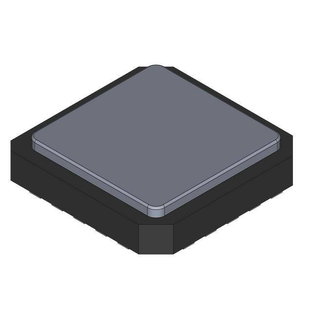


 工商网监
湘ICP备2023018690号
工商网监
湘ICP备2023018690号
