NCP1031POEEVB
NCP1031 6.5 W POE DC-DC
Converter Evaluation Board
User's Manual
http://onsemi.com
EVAL BOARD USER’S MANUAL
Introduction
converters at the load end of the cables which transform the
48 V to logic levels such as 5.0 Vdc or 3.3 Vdc or both, to
power the communications equipment. The PDs should be
able to operate with a maximum average input power of
12.95 W, and should be able to tolerate an input voltage
range of 36 to 57 Vdc. In addition, a certain “protocol” is
required in which the PD is detected (Signature Mode) and
then classified (Classification Mode) according to its
maximum power level.
Signature Detection:
The upstream PSE equipment detects the PD by injecting
two different voltages between 2.8 and 10 Vdc into the PD
input terminals. If the detected impedance of the PD as
measured by the V/I slope is above 23.7 kW, and below
26.25 kW, the PD is considered present. If the impedance is less
than 15 k, or greater than 33 k, the PD is considered not present,
and no further voltage will be applied.
Classification Mode:
To classify the PD according to its intended power level,
the PSE will again source a voltage between 14.5 and
20.5 Vdc to the PD. The classification is determined by the
current drawn by the PD upon application of this voltage,
and is summarized in the Table 1.
A solution to one aspect of Power Over Ethernet (POE) is
presented here utilizing the ON Semiconductor NCP1031
series of monolithic, high voltage switching regulators with
internal MOSFET. The evaluation board user’s manual
provides details for constructing an inexpensive, high
efficiency, 5.0 V DC power supply with a power output of
5.0 to 6.5 W, (output power is conversion mode dependent
− see DC to DC Converter Operation description below).
The associated input circuitry for responding to POE
detection and classification protocol is also included.
ON Semiconductor also can provide a demonstration PC
board with this circuitry upon request.
POE Background
As a result of IEEE Standard 802.3AF, it is now possible
to inject DC power through Ethernet data transmission lines
to power Ethernet communication devices as long as the end
power requirement is less than 13 W. The parametric details
of DC power transmission and the associated terminology is
outlined in this IEEE document. POE consists of two power
entities: Power Sourcing Equipment (PSE) and Powered
Devices (PDs). The PSEs typically provides 48 Vdc
nominal to the LAN cables while the PDs are small DC−DC
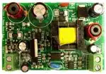
Figure 1. NCP1031 Evaluation Board
© Semiconductor Components Industries, LLC, 2012
October, 2012 − Rev. 2
1
Publication Order Number:
EVBUM2142/D
�NCP1031POEEVB
Table 1. CLASSIFICATION
Class
Pmin
Pmax
Iclass min*
Iclass max*
0
0.44 W
1
0.44 W
2
3
4
Rclass (R4)*
12.95 W
0 mA
4.0 mA
Open
3.84 W
9.0 mA
12 mA
217 W
3.84 W
6.49 W
17 mA
20 mA
135 W
6.49 W
12.95 W
26 mA
30 mA
91 W
TBD
TBD
36 mA
44 mA
62 W
*Note that from the 4th and 5th columns on the table, that the current drawn from the PSE falls between the Iclass minimum and maximum values
for a given power classification. The last column is the value of the resistor (R4) required for classification in the circuit described by this
evaluation board user’s manual.
Additional Input Features
DC to DC Converter Operation
In addition to the signature and classification circuitry, the
PD must also include circuitry to limit the inrush current
from the PSE to 400 mA when the input voltage is applied,
and to prevent any quiescent currents or impedances caused
by the DC-to-DC converter to be ignored during the
signature and classification processes.
The DC-to-DC converter is designed around
ON Semiconductor’s monolithic NCP1031 switching
regulator IC (U2). For a 5.0 W maximum output, the
converter is configured as a discontinuous mode (DCM)
flyback topology with the conventional TL431 and
optocoupler voltage feedback scheme. Modifications to the
transformer design and the control loop compensation
network for continuous conduction mode flyback operation
will allow up to 6.5 W (1.3 A) output. The input utilizes a
differential mode pi filter comprised of C3, L1 and C4.
Control chip startup is accomplished when the undervoltage
terminal at pin 6 exceeds 2.5 V. The resistor divider network
of R7, R8, and R9 sets the chip’s under and overvoltage
levels to 35 and 80 V, respectively. Internal startup bias is
provided thru pin 8, which drives a constant current source
that charges Vcc capacitor C7. Once U2 has started, the
auxiliary winding on transformer T1 (pins 2, 3) provides the
operating bias via diode D4 and resistor R11.
Voltage spikes caused by the leakage inductance of T1 are
clamped by the network of C5, D6 and R10. The actual
power rating on R10 will be a function of the
primary-to-secondary leakage inductance of T1, and the
lower the better. Capacitor C6 sets the switching frequency
of the converter to approximately 220 kHz.
Because of the required secondary isolation, a TL431
(U4) is implemented as an error amplifier along with
optocoupler U3 to create the voltage sensing and feedback
circuitry. The internal error amplifier in U2 has been
disabled by grounding pin 3, the voltage sense pin, and the
amplifier’s output compensation node on pin 4 is utilized to
control the pulse width via the optocoupler’s photo
transistor. The output voltage sense is divided down to the
2.5 V reference level of the TL431 by R16 and R17, and
closed loop bandwidth and phase margins are set by C9 and
R15 for DCM operation. Additional components C14, C15
and R12 are required for feedback loop stabilization if
configured for CCM flyback operation. C8 on the primary
side provides noise decoupling and additional high
frequency roll off for U2. This implementation provides
output regulation better than 0.5% for both line and load
changes, and a closed loop phase margin of better than 50°.
Signature/Classification Circuit Details
Referring to the schematic of Figure 3, the input signature
and classification circuitry is designed around a few discrete
and inexpensive ON Semiconductor parts that include the
TL431 programmable reference, a 2N7002 signal level
MOSFET, a 2N5550 NPN transistor, an NTD12N10
MOSFET and several Zener diodes and a few resistors and
capacitors. For signature detection, a 24.9 K resistor (R1) is
placed directly across the input. Note that during signature
detection, the input voltage is below 10 V and the constant
current source formed by U1, Q2 and R4 is off because of the
9.1 V Zener that must be overcome to bias this circuit. Note
also that MOSFET Q3, which functions as a series input
switch in the return leg of the DC−DC converter, will be off
until the input voltage exceeds approximately 27 V. This
voltage is the sum of D2’s Zener voltage and the gate
threshold of Q3.
As the voltage is ramped up to the classification level, D1
conducts above approximately 9.8 V and the current source
formed by U1, Q2 and resistor R4 turns on and the current
is precisely limited by the reference voltage of U1 (2.5 V)
and the classification resistor R4.
Once classification is verified the input can now ramp up
to the nominal 48 V. Once this voltage exceeds the sum of
Q3’s gate threshold and D2’s Zener voltage, Q3 will start to
turn on. It will not turn on abruptly, however, but will operate
in its linear region momentarily due to the RC time constant
created by R6 and C2. The momentary operation in the
linear region allows for inrush current limiting because Q3
will act like a resistor during this period. D3 clamps the
voltage on Q3’s gate to 15 V, while R5 provides a discharge
path for C2 when the input from the PSE is off. MOSFET Q1
will also turn on at the same voltage level as Q3, and this will
switch off the U1/Q2 current source so as to reduce
additional current drain from the input.
http://onsemi.com
2
�NCP1031POEEVB
turn back on before the inductor current is zero, the peak
switch current is less, so higher power outputs can be
achieved without overcurrent protection intervention. There
is a cost, however, to this latter mode of operation in that the
control loop bandwidth must be made lower with a resulting
poorer transient response to load and line variation. CCM
operation introduces a right half-plane zero to the power
topology response characteristic which may need to be
compensated for with the additional feedback components
shown in Figure 3, if proper feedback stability is to be
achieved. CCM may also generate more EMI due to the fact
that the output rectifier must now be force commutated off.
Output rectifier D5 is a three amp Schottky device for
enhanced efficiency, and the output voltage is filtered by the
pi network comprised of C11, L2 and C12. Typical
peak-to-peak noise and ripple on the output are below
100 mV under all normal load and line conditions. C13
provides for additional high frequency noise attenuation.
Typical input to output efficiency is in the area of 75% at
full load. Higher efficiencies can be achieved by replacing
D5 with a MOSFET based synchronous rectifier circuit
(see ON Semiconductor evaluation board user’s manual,
EVBUM2132/D, for implementing a simple synchronous
rectifier circuit to a flyback topology).
Overcurrent protection is provided by the internal peak
current limit circuit in the NCP1031. The circuit can provide
a continuous output current of 1.3 A at 25°C with surge up
to 1.5 A when configured as a CCM flyback before
overcurrent and/or overtemperature limiting ensues. When
configured for the discontinuous mode, the current is limited
to about 1.0 A with a 1.2 A peak.
0.9
EFFICIENCY (%)
0.8
Magnetics Design
The discontinuous mode flyback transformer design is
detailed in Figure 4 and the continuous mode transformer is
shown in Figure 5. In the design of flyback transformers, it
is essential to keep the windings in single layers and evenly
spread over the window length of the core structure to keep
leakage inductance minimized. In this application, this was
easily achieved, with a small EF16 ferrite core from
Ferroxcube.
0.7
0.6
0.5
0.4
0.3
0
2
4
6
POUT, OUTPUT POWER (W)
Figure 2. Efficiency Versus Output Power Graph
Discontinuous Versus Continuous Mode Operation
References
In discontinuous mode flyback operation, the inductor
current falls to zero before the MOSFET switch is turned on
again. This mode of operation causes the output to have a
first order filter network characteristic and, as a
consequence, feedback loop stabilization is simple and wide
bandwidth for good output transient response can be
achieved. This operational mode, unfortunately results in
higher peak switch currents and limits the power output of
this circuit due to the internal current limit set point and the
thermal protection circuits in the NCP1031. With
continuous current mode operation, where the MOSFET can
1. IEEE Standard 802.3AF (Ethernet power
transmission standards).
2. Power Electronic Technology Magazine, June
2004, Page 45.
3. ON Semiconductor Data Sheet – NCP1030,
NCP1031.
4. On Semiconductor Application Note AND8119,
“Design of an Isolated 2.0 W Bias Supply for
Telecom Systems Using the NCP1030”.
http://onsemi.com
3
8
�−
38−60
Vdc in
+
http://onsemi.com
4
C2
2.2 mF
25 V
+
2N7002
Q1
470 K
TL431
U1
R5
68 K
R4
137
1%
Q3
NTD12N10
D2
24 V
D3
15 V
Q2
2N5550
R6
51 K
+
R9
6.8 K
R8
9.1 K
R7
200 K
C3
10 nF
100 V
8
4
U2
7
5
2
1 3
6
NCP1031
C4
47−68 mF
100 V
1. R1 sets signature impedance (25K nominal).
2. R4 sets the classification current (18.5 mA nominal for Class 2; 6.5 W output max).
3. C10 is optional but will improve stability and reduce conducted EMI.
4. R7, R8, & R9 sets converter input UVL and OVP points.
5. C2 sets inrush current profile.
6. Vout set by R16, R17.
7. Crossed lines on schematic are not connected.
C1
10 nF
100 V
D1
9.1 V
R2
6.2 K
R3 0.5 W
R1
24.9 K
1%
L1
4.7 mH
C6
1 nF
R10
10 K
0.5 W
47 1N4148
D6
MUR110
D4
R11
2
3
4
1
opto
U3
5,6
0.1
C9
R15
3.3 K
R14
1K
R13
180
C11 +
1500 mF
6.3 V
D5
MBR340
7,8
C10
1 nF “Y’’
U4
cap
TL431
C8
10 nF
C7
+ 10 mF
C5
2.2 nF
1 kV
T1
R17
2.2 K
R16
2.2 K
C12 +
100 mF
10 V
L2
4.7 mH
C13
0.1
+
5 V, 1 A
Output
−
NCP1031POEEVB
Figure 3. Schematic for the NCP1031 Evaluation Board
�NCP1031POEEVB
Part Description: 5 W, 200 kHz POE Flyback Transform, 5 VOUT, 48 VIN
Schematic ID: T1
Core Type: Ferroxcube EF16 (E16/8/5); 3C95 Material Or Similar
Core Gap: Gap for 100 mH
Inductance: 90 − 100 mH
Bobbin Type: 8 Pin Horizontal Mount for EF16
Windings (in order):
Winding # / Type
Turns / Material / Gauge / Insulation Data
VCC / BOOST(2 − 3)
9 turns of #28HN spiral wound over 1 layer. Insulate
with 1 layer of tape (250 V insulation to next winding).
Primary(1 − 4)
24 turns of #28HN over 1 layer. Insulate for 1.5 kV to
the next winding.
5 V Secondary (5, 6 − 7, 8)
4 turns of 4 strands of #28HN flat wound over 1 layer
evenly and terminated with 2 strands per pin. Insulate
with tape.
NOTE:
Vendor for this transform is Mesa Power Systems (Escondido, CA). Part# 131297.
Hipot:
1.5 kV from VCC Boost/Primary to Secondary.
Lead Breakout / Pinout
Schematic
(Bottom View − facing pins)
1
8
7
Pri
4
5V sec
4
5
6
5
3
6
2
7
1
8
3
Vcc
2
Figure 4. DCM Flyback Transformer Design
http://onsemi.com
5
�NCP1031POEEVB
Part Description: 6.5 W, 220 kHz POE Flyback Transform, 5 VOUT, 48 VIN
Schematic ID: T1
Core Type: Ferroxcube EF16 (E16/8/5); 3C95 Material Or Similar
Core Gap: Gap for 250 mH
Inductance: 250 $ 15 mH
Bobbin Type: 8 Pin Horizontal Mount for EF16
Windings (in order):
Winding # / Type
Turns / Material / Gauge / Insulation Data
VCC / BOOST(2 − 3)
18 turns of #28HN spiral wound over 1 layer. Insulate
with 1 layer of tape (250 V insulation to next winding).
Primary(1 − 4)
48 turns of #28HN over 2 layer. Insulate for 1.5 kV to
the next winding.
5 V Secondary (5, 6 − 7, 8)
8 turns of 2 strands of #28HN flat wound over 1 layer
evenly and terminated with 2 strands per pin. Insulate
with tape.
NOTE:
Vendor for this transform is Mesa Power Systems (Escondido, CA). Part# 131294.
Hipot:
1.5 kV from VCC Boost/Primary to Secondary.
Lead Breakout / Pinout
Schematic
(Bottom View − facing pins)
1
8
7
Pri
4
5V sec
4
5
6
5
3
6
2
7
1
8
3
Vcc
2
Figure 5. CCM Flyback Transformer Design
http://onsemi.com
6
�NCP1031POEEVB
TEST PROCEDURE
Introduction
3. Adjust the bench supply to 5.00 volts output. The
input current meter to the evaluation board should
read between 0.190 mA and 0.230 mA. Both
evaluation board output meters should read
essentially zero.
4. Adjust the bench supply to 18.00 Vdc output. The
input current to the board under test should read
between 17 and 21 mA.
5. Adjust the bench supply to 48 Vdc output and the
converter should start and show an output voltage
of 4.9 to 5.1 Vdc. The scope should show less than
50 mV ripple and indicate output stability by a
constant, non-jittering trace.
6. Adjust the electronic load slowly from zero to
1.3 amps as evidenced by the output current meter.
The output should still be between 4.9 and
5.1 volts and the ripple on the scope should be less
than 100 mV and indicate a stable output
throughout this load range.
7. With 1.3 amps on the output check the input
current and make sure it’s below 200 mA
(efficiency check.)
8. Adjust the bench supply slowly down to
approximately 35 Vdc. The converter should shut
off between 34 and 36 Vdc and the output will go
to zero. Adjust the input back to 38 Vdc and the
converter should come back on with normal
output.
9. Adjust the input voltage back to 48 Vdc and then
slowly increase the load to over 1.5 amps. The
output voltage should start collapsing around 1.4
to 1.6 amps indicating current limiting.
10. Set the current back to 1.3 amps and allow the
evaluation board to run for about 5 minutes to
assure that it doesn’t thermally limit by shutting
down. Note: This last test may not be necessary
after several evaluation boards and the test
procedure are validated.
11. Turn the bench supply off and disconnect the
evaluation board. Testing is complete.
The POE (Power Over the Ethernet) evaluation board is
a 6.5 W DC−DC converter using the ON Semiconductor
NCP1031 monolithic controller/mosfet chip in a flyback
topology. The input is 48 Vdc nominal and the output is
5 Vdc at 1.3 A maximum. There is additional input circuitry
that responds to Ethernet protocol defined as “Signature”
and “Classification” detection. Signature just indicates that
the power supply does exist and classification allows the
upstream Power Sourcing Equipment (PSE) to determine
the rated power level of the supply or Powered Device (PD).
Both of these detection modes are performed at low input
voltages in which the main converter does not operate. The
converter will only come on with Vin above 35 Vdc.
Equipment Required
1. Adjustable bench power supply capable of up to
50 Vdc with an output current of up to 0.5 amps.
2. Digital volt/amp meters to measure input and
output current and voltage to the evaluation board.
3. A variable electronic load or rheostat capable of
up to a 2 amp load.
4. Oscilloscope with probe to monitor output ripple
on the demo converter.
Setup Procedure
Set the equipment as shown in the Figure 6 so that the
input and output voltage and current to the evaluation board
can be measured and the output ripple can be monitored.
Test Procedure
1. Switch the electronic load on and set to zero load;
switch all of the digital meters on (assuming they
are wired properly for voltage and current
sensing); turn the oscilloscope on with sensing in
AC mode and 50 mV per division vertical and a
sweep rate of 5 mS per division. Connect the scope
probe to the evaluation board’s output terminals.
2. Set the voltage adjust to zero on the bench supply
and switch it on.
Bench Supply
48.000 V
Vadj
Iadj
0.00 A
+ −
I
+−
Digital Meter
V
Electronic Load
A
Load Adj.
+ −
Digital Meter
I
+−
Eval. Board
under Test
In
Out
V
+−
V
+−
Figure 6. Setup Procedure Diagram
http://onsemi.com
7
O’scope
�NCP1031POEEVB
Table 2. BILL OF MATERIAL FOR THE NCP1031 EVALUATION BOARD
Designator
Qty.
Description
Value
Tolerance
Footprint
Manufacturer
Manufacturer
Part Number
Substitution
Allowed
Lead
Free
D1
1
Zener Diode
9.1 V
NA
SOD−123
ON Semiconductor
MMSZ5239BT1,G
No
Yes
D6
1
Ultrafast Rectifier
1 A, 100 V
NA
SMA/SMB
ON Semiconductor
MURS110T3
No
Yes
D5
1
Schottky Rectifier
1 A, 40 V
NA
SMC
ON Semiconductor
MBRS340T3,G
No
Yes
D3
1
Zener Diode
15 V
5%
SOD−123
ON Semiconductor
MMSZ5245BT1,G
No
Yes
D2
1
Zener Diode
5%
SOD−123
ON Semiconductor
No
Yes
D4
1
Diode
100 V
NA
SOD−123
ON Semiconductor
MMSD4148,G
No
Yes
Q2
1
NPN Transistor
100 V
NA
SOT−23
ON Semiconductor
MMBT5550L,G
No
Yes
Q1
1
MOSFET
60 V, 115 mA
NA
SOT−23
ON Semiconductor
2N7002LT,G
No
Yes
Q3
1
Power MOSFET
100 V, 12 A
NA
DPAK−3
ON Semiconductor
NTD12N10
No
Yes
U1, U4
2
Programmable Zener
2.5−36 V
1%
SOIC−8
ON Semiconductor
TL431ACD
No
Yes
U3
1
Optocoupler
NA
NA
4 Pin
Vishay
SFH615A−4
No
Yes
U2
1
Integrated Controller
NA
NA
SO−8
ON Semiconductor
NCP1031DR2G
No
Yes
C10
1
WYO “Y” Cap
1.0 nF
20%
LS = 0.25″
Vishay
WYO102MCMBF0KR
No
Yes
24 V
28 V
MMSZ5252BT1,G
MMSZ5255BT1,G
C6
1
Ceramic Capacitor
1.0 nF, 100 V
5%
0805
AVX
08051C102JAT2A
Yes
Yes
C1, C3, C8
3
Ceramic Capacitor
10 nF, 100 V
5%
0805
AVX
08051C103JAT2A
Yes
Yes
C9, C13
2
Ceramic Capacitor
0.1 mF, 50 V
10%
0805
AVX
08055C104JAT2A
Yes
Yes
C5
1
Ceramic Capacitor
2.2 nF, 1.0 kV
20%
LS = 0.25″
Vishay
562R5GAD22
Yes
Yes
C4
1
Electrolytic Capacitor
47 mF or 60 mF,
100 V
20%
LS = 0.2″
Rubycon, UCC
100 NA47M 10×20
Yes
Yes
C11
1
Electrolytic Capacitor
1,000 to 1,500 mF,
6.3 V
20%
LS = 0.15″
Rubycon, UCC
6.3 NA1000M 10×16
Yes
Yes
C12
1
Electrolytic Capacitor
100 mF, 10 V
20%
LS = 0.1″
Rubycon, UCC
10 NA100M 6.3×11
Yes
Yes
C7
1
Electrolytic Capacitor
10 mF, 16 V
20%
LS = 0.1″
Rubycon, UCC
16 TWL10M 4×7
Yes
Yes
C2
1
Electrolytic Capacitor
1.0 mF to 2.2 mF,
35 V
20%
LS = 0.1″
Rubycon, UCC
50 TWL1M 5×11
Yes
Yes
R10
1
Resistor
10 kW, 1/2 W
5%
2010
Vishay
CRCW2010−10K
Yes
Yes
R2
1
Resistor
6.2 kW, 1/2 W
5%
2010
Vishay
CRCW2010−6.19K
Yes
Yes
R4
1
Resistor
137 W, 1/4 W
1%
0805
Vishay
CRCW0805−137
Yes
Yes
R1
1
Resistor
24.9 kW, 1/4 W
1%
0805
Vishay
CRCW0805−24.9K
Yes
Yes
R11
1
Resistor
47 W, 1/4 W
1%
0805
Vishay
CRCW0805−47
Yes
Yes
R13
1
Resistor
180 W, 1/4 W
1%
0805
Vishay
CRCW0805−180
Yes
Yes
R14
1
Resistor
1.0 kW, 1/4 W
1%
0805
Vishay
CRCW0805−1.0K
Yes
Yes
R16, R17
2
Resistor
2.2 kW, 1/4 W
1%
0805
Vishay
CRCW0805−2.2K
Yes
Yes
R9
1
Resistor
6.8 kW, 1/4 W
1%
0805
Vishay
CRCW0805−6.81K
Yes
Yes
R8
1
Resistor
9.1 kW, 1/4 W
1%
0805
Vishay
CRCW0805−9.09K
Yes
Yes
Not Used
0
Resistor (Not Used)
10 kW, 1/4 W
1%
0805
Vishay
CRCW0805−10K
Yes
Yes
R15
1
Resistor
3.3 kW, 1/4 W
1%
0805
Vishay
CRCW0805−3.3K
Yes
Yes
R6
1
Resistor
51 kW, 1/4 W
1%
0805
Vishay
CRCW0805−51.1K
Yes
Yes
R5
1
Resistor
68 kW, 1/4 W
1%
0805
Vishay
CRCW0805−68.1K
Yes
Yes
R7
1
Resistor
200 kW, 1/4 W
1%
0805
Vishay
CRCW0805−200K
Yes
Yes
R3
1
Resistor
470 kW, 1/4 W
1%
0805
Vishay
CRCW0805−470K
Yes
Yes
L1, L2
2
Inductor
4.7 mH, 3.0 A
NA
LS = 0.4″
Coilcraft
PCV−0−472−03
No
Yes
T1
1
Transformer, 10 W
Flyback (Custom)
NA
NA
TH
Mesa Power
Systems
13−1269
No
No
Input,
Output
2
Terminal Blocks
−
−
5.08 mm
Pitch
On Shore
Technology Inc.
OSTYC022150−ND
Yes
Yes
http://onsemi.com
8
�onsemi,
, and other names, marks, and brands are registered and/or common law trademarks of Semiconductor Components Industries, LLC dba “onsemi” or its affiliates
and/or subsidiaries in the United States and/or other countries. onsemi owns the rights to a number of patents, trademarks, copyrights, trade secrets, and other intellectual property. A
listing of onsemi’s product/patent coverage may be accessed at www.onsemi.com/site/pdf/Patent−Marking.pdf. onsemi is an Equal Opportunity/Affirmative Action Employer. This
literature is subject to all applicable copyright laws and is not for resale in any manner.
The evaluation board/kit (research and development board/kit) (hereinafter the “board”) is not a finished product and is not available for sale to consumers. The board is only intended
for research, development, demonstration and evaluation purposes and will only be used in laboratory/development areas by persons with an engineering/technical training and familiar
with the risks associated with handling electrical/mechanical components, systems and subsystems. This person assumes full responsibility/liability for proper and safe handling. Any
other use, resale or redistribution for any other purpose is strictly prohibited.
THE BOARD IS PROVIDED BY ONSEMI TO YOU “AS IS” AND WITHOUT ANY REPRESENTATIONS OR WARRANTIES WHATSOEVER. WITHOUT LIMITING THE FOREGOING,
ONSEMI (AND ITS LICENSORS/SUPPLIERS) HEREBY DISCLAIMS ANY AND ALL REPRESENTATIONS AND WARRANTIES IN RELATION TO THE BOARD, ANY
MODIFICATIONS, OR THIS AGREEMENT, WHETHER EXPRESS, IMPLIED, STATUTORY OR OTHERWISE, INCLUDING WITHOUT LIMITATION ANY AND ALL
REPRESENTATIONS AND WARRANTIES OF MERCHANTABILITY, FITNESS FOR A PARTICULAR PURPOSE, TITLE, NON−INFRINGEMENT, AND THOSE ARISING FROM A
COURSE OF DEALING, TRADE USAGE, TRADE CUSTOM OR TRADE PRACTICE.
onsemi reserves the right to make changes without further notice to any board.
You are responsible for determining whether the board will be suitable for your intended use or application or will achieve your intended results. Prior to using or distributing any systems
that have been evaluated, designed or tested using the board, you agree to test and validate your design to confirm the functionality for your application. Any technical, applications or
design information or advice, quality characterization, reliability data or other services provided by onsemi shall not constitute any representation or warranty by onsemi, and no additional
obligations or liabilities shall arise from onsemi having provided such information or services.
onsemi products including the boards are not designed, intended, or authorized for use in life support systems, or any FDA Class 3 medical devices or medical devices with a similar
or equivalent classification in a foreign jurisdiction, or any devices intended for implantation in the human body. You agree to indemnify, defend and hold harmless onsemi, its directors,
officers, employees, representatives, agents, subsidiaries, affiliates, distributors, and assigns, against any and all liabilities, losses, costs, damages, judgments, and expenses, arising
out of any claim, demand, investigation, lawsuit, regulatory action or cause of action arising out of or associated with any unauthorized use, even if such claim alleges that onsemi was
negligent regarding the design or manufacture of any products and/or the board.
This evaluation board/kit does not fall within the scope of the European Union directives regarding electromagnetic compatibility, restricted substances (RoHS), recycling (WEEE), FCC,
CE or UL, and may not meet the technical requirements of these or other related directives.
FCC WARNING – This evaluation board/kit is intended for use for engineering development, demonstration, or evaluation purposes only and is not considered by onsemi to be a finished
end product fit for general consumer use. It may generate, use, or radiate radio frequency energy and has not been tested for compliance with the limits of computing devices pursuant
to part 15 of FCC rules, which are designed to provide reasonable protection against radio frequency interference. Operation of this equipment may cause interference with radio
communications, in which case the user shall be responsible, at its expense, to take whatever measures may be required to correct this interference.
onsemi does not convey any license under its patent rights nor the rights of others.
LIMITATIONS OF LIABILITY: onsemi shall not be liable for any special, consequential, incidental, indirect or punitive damages, including, but not limited to the costs of requalification,
delay, loss of profits or goodwill, arising out of or in connection with the board, even if onsemi is advised of the possibility of such damages. In no event shall onsemi’s aggregate liability
from any obligation arising out of or in connection with the board, under any theory of liability, exceed the purchase price paid for the board, if any.
The board is provided to you subject to the license and other terms per onsemi’s standard terms and conditions of sale. For more information and documentation, please visit
www.onsemi.com.
PUBLICATION ORDERING INFORMATION
LITERATURE FULFILLMENT:
Email Requests to: orderlit@onsemi.com
onsemi Website: www.onsemi.com
◊
TECHNICAL SUPPORT
North American Technical Support:
Voice Mail: 1 800−282−9855 Toll Free USA/Canada
Phone: 011 421 33 790 2910
www.onsemi.com
1
Europe, Middle East and Africa Technical Support:
Phone: 00421 33 790 2910
For additional information, please contact your local Sales Representative
�


 工商网监
湘ICP备2023018690号
工商网监
湘ICP备2023018690号
