NLAS2750
Low Voltage Dual SPDT
Analog Switch with
Negative Swing Audio
Capability
www.onsemi.com
The NLAS2750 is a dual SPDT low on−resistance analog switch. It
can operate from a single 1.8 V to 5.0 V power supply. It is a
bi−directional switch that can switch a negative voltage swing audio
signal without requiring a coupling capacitor. With a single power
supply, the audio signal can swing over the range from −2.5 V to VCC.
MARKING
DIAGRAM
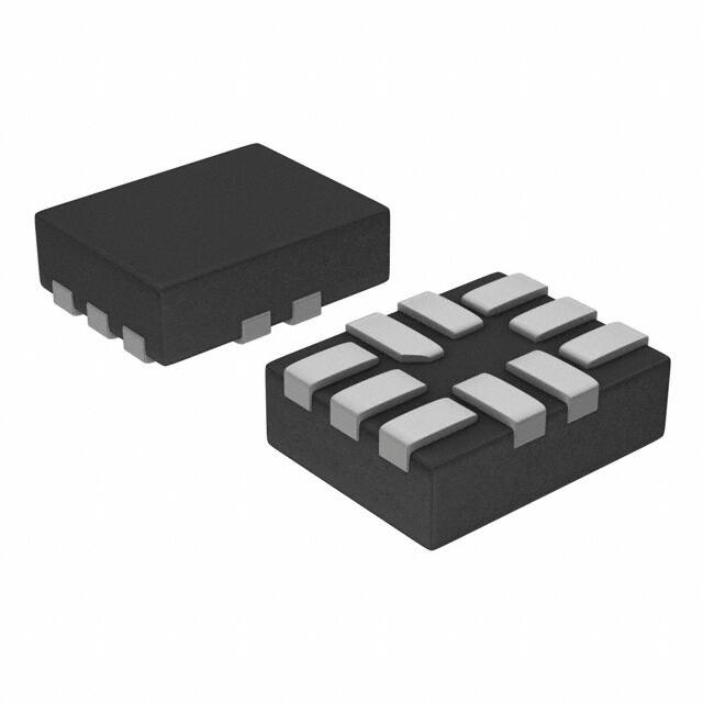
UQFN10
CASE 488AT
Features
1
ALMG
G
• Capable to Switch Negative Swing Audio Signals Without Requiring
a DC Blocking Capacitor
AL
M
G
• Low On−resistance (RON)
• Low Voltage Digital Control Logic:
•
•
•
= Specific Device Code
= Date Code/Assembly Location
= Pb−Free Device
(Note: Microdot may be in either location)
(VINH = 1.4 V @ VCC = 2.7 V to 4.3 V)
Low Power Consumption (ICC ≤ 250 nA)
Space Saving 1.4 mm x 1.8 mm Package UQFN Package
This is a Pb−Free Device
NC2
GND
7
6
Typical Applications
• Cellular Phones
• Portable Media Players
IN2
8
5
NC1
COM2
9
4
IN1
10
3
COM1
NO2
1
2
VCC
NO1
FUNCTION TABLE
IN1 (Pin 4)
IN2 (Pin 8)
Function
0
X
COM1 = NC1
1
X
COM1 = NO1
X
0
COM2 = NC2
X
1
COM2 = NO2
ORDERING INFORMATION
See detailed ordering and shipping information on page 7 of
this data sheet.
© Semiconductor Components Industries, LLC, 2015
April, 2015 − Rev. 3
1
Publication Order Number:
NLAS2750/D
�NLAS2750
COM
NO
NC
IN
Figure 1. Logic Equivalent Circuit
MAXIMUM RATINGS
Symbol
Parameter
Value
Unit
−0.3 to +6.5
V
Min. VIS = VCC − 6.5 V or
−2.5 V (whichever is greater)
Max. VIS = VCC + 0.3 V
V
−0.3 to +6.5
V
50
mA
VCC
Positive DC Supply Voltage
VIS
Analog Input Voltage (COM, NO, NC) (Notes 1 and 2)
VIN
Digital (IN1, IN2)
ICC
Current (GND, VCC)
IIS
Continuous Switch Current (COM, NO, NC) (Note 1)
±250
mA
IISP
Peak Switch Current (Pulsed at 1 ms, 10% Duty Cycle)
±500
mA
−65 to +150
°C
200
mW
TSTG
PD
VESD
ILU
Storage Temperature
Power Dissipation
ESD (Human Body Model)
All pins
I/O to GND
kV
6
8
Latch−up (per JESD78)
300
mA
Stresses exceeding those listed in the Maximum Ratings table may damage the device. If any of these limits are exceeded, device functionality
should not be assumed, damage may occur and reliability may be affected.
1. Signals on COM, NO, NC, exceeding VCC will be clamped by internal diodes. Limit forward diode current to maximum current ratings.
2. The algebraic convention whereby the most negative value is a minimum and the most positive a maximum is used in this data sheet.
RECOMMENDED OPERATING CONDITIONS
Symbol
Parameter
Min
Max
Unit
1.8
5.5
V
VCC
Power Supply Range
VIN
Digital Select Input Voltage Overvoltage Tolerance (OVT) (IN1, IN2)
GND
5.5
V
VIS
Analog Input Voltage (NC, NO, COM) (Note 3)
−2.5
VCC
V
TA
Operating Temperature Range
−40
+85
°C
tr, tf
Input Rise or Fall Time (IN1, IN2)
VCC < 2.7 V
VCC ≥ 2.7 V
ns/V
20
10
Functional operation above the stresses listed in the Recommended Operating Ranges is not implied. Extended exposure to stresses beyond
the Recommended Operating Ranges limits may affect device reliability.
3. The voltage across the switch should be ≤ 5.5 V.
www.onsemi.com
2
�NLAS2750
ELECTRICAL CHARACTERISTICS (VCC = 2.7 V, ±10%) (Note 4)
Guaranteed Maximum Limit
−405C to 855C
Symbol
Parameter
Test Conditions
Min
Typ
Max
Unit
ANALOG SWITCH
VIS
RDS(on)
�RON
Analog Signal Range (Note 5)
−2.5
On−Resistance
On−Resistance Match
RON Flatness
On−Resistance Resistance
Flatness
INO/NC(off)
Switch Off Leakage Current
0.6
VCC = 2.7 V,
VIS = (VCC − 4.5 V), −1 V, 0 V
1 V, 2 V, VCC
IIS = 100 mA
VCC = 2.7 V,
VNC/NO = −2.5 V or 2.5 V,
VCOM = 2.5 V or −2.5 V
ICOM(off)
ICOM(on)
Channel On Leakage Current
VCC
V
1.3
�
0.1
�
0.37
�
50
nA
50
±250
nA
±250
nA
DIGITAL CONTROL
VINH
Input Voltage High
VCC = 5 V
VCC = 2.7 V to 4.3 V
VINL
Input Voltage Low
VCC = 2.7 V to 5 V
CIN
Input Capacitance
IINL or IINH
1.6
1.4
V
0.6
5
Input Current
VIN = 0 or VCC
V
pF
±1
�A
±250
nA
POWER CONSUMPTION
ICC
Maximum Quiescent Supply
Current
VCC = 2.7 V to 4.3 V
50
Product parametric performance is indicated in the Electrical Characteristics for the listed test conditions, unless otherwise noted. Product
performance may not be indicated by the Electrical Characteristics if operated under different conditions.
4. Typical values are measured at 25°C and are for design aid only, not guaranteed nor subject to production testing.
5. Guaranteed by design, not subject to production testing.
DYNAMIC CHARACTERISTICS (VCC = 2.7 V, ±10%) (Note 4)
Guaranteed Maximum Limit
−405C to 855C
Symbol
tBBM
Parameter
Test Conditions
Break−Before−Make Time
(Notes 6 and 7)
tON(EN)
Enable Turn−On Time
(Notes 6 and 7)
tOFF(EN)
Enable Turn−Off Time
(Notes 6 and 7)
VCC = 2.7 V, VIS = 1.5 V,
RL = 50 �, CL = 35 pF
QINJ
Charge Injection (Note 6)
CL = 1 nF, RGEN = 0 �,
VGEN = 0 V
OIRR
Off−Isolation (Note 6)
XTALK
Crosstalk (Notes 6 and 8)
BW
CNC/NO(off)
Bandwidth (Note 6)
Min
Typ
1000
1250
Max
Unit
ns
80
150
ns
110
130
ns
60
pC
VCC = 2.7 V, RL = 50 �,
CL = 5 pF, f = 300 kHz
−58
dB
−61
dB
VCC = 2.7 V, RL = 50 �, −3 dB
44
MHz
25
pF
75
pF
Channel−Off Capacitance
(Note 6)
VCC = 2.7 V, f = 1 MHz
CCOM/NC/NO(on) Channel−On Capacitance
(Note 6)
6. Guaranteed by design, not subject to production testing.
7. VIS = input voltage to perform proper function.
8. Crosstalk Measured between channels.
www.onsemi.com
3
�NLAS2750
TYPICAL CHARACTERISTICS
2
1.2
1.8
1.1
1.6
1
RON, ON RESISTANCE (�)
RON, ON RESISTANCE (�)
(25°C, unless otherwise specified)
1.4
1.2
+85°C
1
0.8
+25°C
−40°C
0.6
0.4
VCC = 2 V
ION = 100 mA
0.2
0
−2.5
−1.5
−0.5
0.5
1.5
+85°C
0.9
0.8
+25°C
0.7
−40°C
0.6
0.5
0.4
0.3
VCC = 2.7 V
ION = 100 mA
0.2
0.1
−2.5
2.5
−1.5
VIS, ANALOG VOLTAGE (V)
2.5
1.1
+85°C
0.9
0.8
0.7
+25°C
0.6
−40°C
0.5
0.4
0.3
VCC = 3.6 V
ION = 100 mA
0.2
−1.5
−0.5
0.5
1.5
RON, ON RESISTANCE (�)
RON, ON RESISTANCE (�)
1.5
1.2
1.1
0.1
−2.5
0.5
VIS, ANALOG VOLTAGE (V)
1.2
1
−0.5
1
+85°C
0.9
0.8
0.7
+25°C
0.6
0.5
−40°C
0.4
0.3
VCC = 4.3 V
ION = 100 mA
0.2
0.1
−2.5
2.5
VIS, ANALOG VOLTAGE (V)
−1.5
−0.5
0.5
1.5
VIS, ANALOG VOLTAGE (V)
Figure 2. On Resistance (RON) vs. Analog Input Voltage (VIS)
www.onsemi.com
4
2.5
�NLAS2750
TYPICAL CHARACTERISTICS
(25°C, unless otherwise specified)
0
−1
GAIN (dB)
−2
−3
−4
−5
−6
−7
−8
1.00E+05
1.00E+06
1.00E+07
1.00E+08
1.00E+09
FREQUENCY (Hz)
Figure 3. Bandwidth Measurement − Gain vs.
Frequency
0
OFF ISOLATION (dB)
−10
−20
−30
−40
−50
−60
−70
−80
1.00E+05
1.00E+06
1.00E+07
1.00E+08
1.00E+09
FREQUENCY (Hz)
Figure 4. Off Isolation Measurement
0
CROSS TALK (dB)
−10
−20
−30
−40
−50
−60
−70
−80
1.00E+05
1.00E+06
1.00E+07
1.00E+08
FREQUENCY (Hz)
Figure 5. Cross Talk Measurement
www.onsemi.com
5
1.00E+09
�NLAS2750
TEST CIRCUITS
VCC
DUT
VIS
Input
Output
GND
VOUT
0.1 �F
50 �
tBMM
35 pF
90%
90% of VOH
Output
Switch Select Pin
GND
Figure 6. tBBM (Time Break−Before−Make)
VCC
Input
DUT
VIS
0.1 �F
50%
Output
VOUT
Open
50%
0V
50 �
VOH
90%
35 pF
90%
Output
VOL
Input
tON
tOFF
Figure 7. tON/tOFF
VCC
VCC
Input
DUT
Output
50 �
50%
0V
VOUT
Open
50%
VOH
35 pF
Output
Input
tOFF
Figure 8. tON/tOFF
www.onsemi.com
6
10%
10%
VOL
tON
�NLAS2750
50 �
DUT
Reference
Transmitted
Input
Output
50 � Generator
50 �
Channel switch control/s test socket is normalized. Off isolation is measured across an off channel. On loss is
the bandwidth of an On switch. VISO, Bandwidth and VONL are independent of the input signal direction.
ǒVVOUT
Ǔ for VIN at 100 kHz
IN
VOUT
Ǔ for VIN at 100 kHz to 50 MHz
VONL = On Channel Loss = 20 Logǒ
VIN
VISO = Off Channel Isolation = 20 Log
Bandwidth (BW) = the frequency 3 dB below VONL
VCT = Use VISO setup and test to all other switch analog input/outputs terminated with 50 �
Figure 9. Off Channel Isolation/On Channel Loss (BW)/Crosstalk
(On Channel to Off Channel)/VONL
DUT
VCC
VIN
Output
Open
GND
CL
Output
Off
VIN
On
Off
�VOUT
Figure 10. Charge Injection: (Q)
ORDERING INFORMATION
Device
NLAS2750MUTAG
Package
Shipping†
UQFN10
(Pb−Free)
3000 / Tape & Reel
†For information on tape and reel specifications, including part orientation and tape sizes, please refer to our Tape and Reel Packaging
Specifications Brochure, BRD8011/D.
www.onsemi.com
7
�MECHANICAL CASE OUTLINE
PACKAGE DIMENSIONS
UQFN10 1.4x1.8, 0.4P
CASE 488AT−01
ISSUE A
DATE 01 AUG 2007
1
SCALE 5:1
EDGE OF PACKAGE
D
ÉÉÉ
ÉÉÉ
ÉÉÉ
PIN 1 REFERENCE
2X
2X
A
0.10 C
L1
E
0.10 C
B
TOP VIEW
A1
0.05 C
A1
C
SIDE VIEW
3
9X
EXPOSED Cu
A
0.05 C
10X
DETAIL A
Bottom View
(Optional)
5
ÉÉÉ
ÉÉÉ
SEATING
PLANE
DETAIL B
Side View
(Optional)
6
e
1
10
10 X
L3
b
A3
DIM
A
A1
A3
b
D
E
e
L
L1
L3
MILLIMETERS
MIN
MAX
0.45
0.60
0.00
0.05
0.127 REF
0.15
0.25
1.40 BSC
1.80 BSC
0.40 BSC
0.30
0.50
0.00
0.15
0.40
0.60
GENERIC
MARKING DIAGRAM*
XXMG
G
e/2
L
MOLD CMPD
NOTES:
1. DIMENSIONING AND TOLERANCING PER ASME
Y14.5M, 1994.
2. CONTROLLING DIMENSION: MILLIMETERS
3. DIMENSION b APPLIES TO PLATED TERMINAL
AND IS MEASURED BETWEEN 0.25 AND 0.30 MM
FROM TERMINAL.
4. COPLANARITY APPLIES TO THE EXPOSED PAD
AS WELL AS THE TERMINALS.
XX
= Specific Device Code
M
= Date Code
G
= Pb−Free Package
(Note: Microdot may be in either location)
0.10 C A B
0.05 C
*This information is generic. Please refer to
device data sheet for actual part marking.
Pb−Free indicator, “G” or microdot “ G”,
may or may not be present.
NOTE 3
BOTTOM VIEW
MOUNTING FOOTPRINT
1.700
0.0669
0.663
0.0261
0.200
0.0079
9X
0.563
0.0221
1
2.100
0.0827
0.400
0.0157
PITCH
DOCUMENT NUMBER:
DESCRIPTION:
10 X
0.225
0.0089
SCALE 20:1
98AON22493D
mm Ǔ
ǒinches
Electronic versions are uncontrolled except when accessed directly from the Document Repository.
Printed versions are uncontrolled except when stamped “CONTROLLED COPY” in red.
10 PIN UQFN, 1.4 X 1.8, 0.4P
PAGE 1 OF 1
ON Semiconductor and
are trademarks of Semiconductor Components Industries, LLC dba ON Semiconductor or its subsidiaries in the United States and/or other countries.
ON Semiconductor reserves the right to make changes without further notice to any products herein. ON Semiconductor makes no warranty, representation or guarantee regarding
the suitability of its products for any particular purpose, nor does ON Semiconductor assume any liability arising out of the application or use of any product or circuit, and specifically
disclaims any and all liability, including without limitation special, consequential or incidental damages. ON Semiconductor does not convey any license under its patent rights nor the
rights of others.
© Semiconductor Components Industries, LLC, 2019
www.onsemi.com
�onsemi,
, and other names, marks, and brands are registered and/or common law trademarks of Semiconductor Components Industries, LLC dba “onsemi” or its affiliates
and/or subsidiaries in the United States and/or other countries. onsemi owns the rights to a number of patents, trademarks, copyrights, trade secrets, and other intellectual property.
A listing of onsemi’s product/patent coverage may be accessed at www.onsemi.com/site/pdf/Patent−Marking.pdf. onsemi reserves the right to make changes at any time to any
products or information herein, without notice. The information herein is provided “as−is” and onsemi makes no warranty, representation or guarantee regarding the accuracy of the
information, product features, availability, functionality, or suitability of its products for any particular purpose, nor does onsemi assume any liability arising out of the application or use
of any product or circuit, and specifically disclaims any and all liability, including without limitation special, consequential or incidental damages. Buyer is responsible for its products
and applications using onsemi products, including compliance with all laws, regulations and safety requirements or standards, regardless of any support or applications information
provided by onsemi. “Typical” parameters which may be provided in onsemi data sheets and/or specifications can and do vary in different applications and actual performance may
vary over time. All operating parameters, including “Typicals” must be validated for each customer application by customer’s technical experts. onsemi does not convey any license
under any of its intellectual property rights nor the rights of others. onsemi products are not designed, intended, or authorized for use as a critical component in life support systems
or any FDA Class 3 medical devices or medical devices with a same or similar classification in a foreign jurisdiction or any devices intended for implantation in the human body. Should
Buyer purchase or use onsemi products for any such unintended or unauthorized application, Buyer shall indemnify and hold onsemi and its officers, employees, subsidiaries, affiliates,
and distributors harmless against all claims, costs, damages, and expenses, and reasonable attorney fees arising out of, directly or indirectly, any claim of personal injury or death
associated with such unintended or unauthorized use, even if such claim alleges that onsemi was negligent regarding the design or manufacture of the part. onsemi is an Equal
Opportunity/Affirmative Action Employer. This literature is subject to all applicable copyright laws and is not for resale in any manner.
PUBLICATION ORDERING INFORMATION
LITERATURE FULFILLMENT:
Email Requests to: orderlit@onsemi.com
onsemi Website: www.onsemi.com
◊
TECHNICAL SUPPORT
North American Technical Support:
Voice Mail: 1 800−282−9855 Toll Free USA/Canada
Phone: 011 421 33 790 2910
Europe, Middle East and Africa Technical Support:
Phone: 00421 33 790 2910
For additional information, please contact your local Sales Representative
�


 工商网监
湘ICP备2023018690号
工商网监
湘ICP备2023018690号
