NLSX4014
4-Bit 100 Mb/s Configurable
Dual-Supply Level
Translator
The NLSX4014 is a 4−bit configurable dual−supply bidirectional
level translator without a direction control pin. The I/O VCC− and I/O
VL−ports are designed to track two different power supply rails, VCC
and VL respectively. The VCC supply rail is configurable from 1.3 V
to 4.5 V while the VL supply rail is configurable from 0.9 V to (VCC
− 0.4) V. This allows lower voltage logic signals on the VL side to be
translated into higher voltage logic signals on the VCC side, and
vice−versa. Both I/O ports are auto−sensing; thus, no direction pin is
required.
The Output Enable (EN) input, when Low, disables both I/O ports
by putting them in 3−state. This significantly reduces the supply
currents from both VCC and VL. The EN signal is designed to track
VL.
Features
•
•
•
•
•
•
•
MARKING
DIAGRAMS
UQFN12
MU SUFFIX
CASE 523AE
1
Wide Low−Side VL Operating Range: 0.9 V to (VCC − 0.4) V
Power Supply Isolation
♦ All Outputs are in the High Impedance State if Either VL or VCC
is at Ground
High−Speed with 100 Mb/s Guaranteed Date Rate for VL > 1.6 V
Low Bit−to−Bit Skew
Overvoltage Tolerant Enable and I/O Pins
Non−preferential Powerup Sequencing
Small packaging: 1.7 mm x 2.0 mm UQFN12
NLV Prefix for Automotive and Other Applications Requiring
Unique Site and Control Change Requirements; AEC−Q100
Qualified and PPAP Capable
These are Pb−Free Devices
WAMG
G
WA = Specific Device Code
M = Date Code
G
= Pb−Free Package
(Note: Microdot may be in either location)
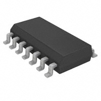
14
SOIC−14
D SUFFIX
CASE 751A
14
• Wide High−Side VCC Operating Range: 1.3 V to 4.5 V
•
www.onsemi.com
1
NLSX4014G
AWLYWW
1
14
TSSOP−14
DT SUFFIX
CASE 948G
14
1
1
NLSX
4014
ALYWG
G
A
=
Assembly Location
L, WL
=
Wafer Lot
Y, YY
=
Year
W, WW =
Work Week
G or G
= Pb−Free Package
(Note: Microdot may be in either location)
ORDERING INFORMATION
Typical Applications
• Mobile Phones, PDAs, Other Portable Devices
Device
Package
Shipping†
NLSX4014MUTAG
UQFN12 3000/Tape & Reel
(Pb−Free)
NLVSX4014MUTAG
UQFN12 3000/Tape & Reel
(Pb−Free)
NLSX4014DR2G
SO−14
2500/Tape & Reel
(Pb−Free)
NLSX4014DTR2G
TSSOP14 2500/Tape & Reel
(Pb−Free)
†For information on tape and reel specifications,
including part orientation and tape sizes, please
refer to our Tape and Reel Packaging Specification
Brochure, BRD8011/D.
© Semiconductor Components Industries, LLC, 2015
December, 2015 − Rev. 5
1
Publication Order Number:
NLSX4014/D
�NLSX4014
VL
1
14
EN
EN
11
VCC
I/O VL1
2
13
VCC
2
10
I/O VCC1
I/O VL2
3
12
I/O VCC1
I/O VL2
3
9
I/O VCC2
I/O VL3
4
11
I/O VCC2
I/O VL3
4
8
I/O VCC3
I/O VL4
5
10
I/O VCC3
I/O VL4
5
7
I/O VCC4
NC
6
9
NC
GND
7
8
I/O VCC4
VL
1
I/O VL1
12
6
GND
(Top View)
Figure 1. Pin Assignments
VL
EN
VCC GND
I/O VL1
I/O VCC1
I/O VL2
I/O VCC2
I/O VL3
I/O VCC3
I/O VL4
I/O VCC4
Figure 2. Logic Diagram
PIN ASSIGNMENT
Pins
FUNCTION TABLE
Description
EN
Operating Mode
VCC
VCC Input Voltage
L
Hi−Z
VL
VL Input Voltage
H
I/O Buses Connected
GND
Ground
EN
Output Enable
I/O VCCn
I/O Port, Referenced to VCC
I/O VLn
I/O Port, Referenced to VL
www.onsemi.com
2
�NLSX4014
P
One−Shot
VL
+1.8V
+3.6V
VL
+1.8 V System
4 kW
VCC
NLSX4014
N
One−Shot
+3.6 V System
I/O VL
I/O1
I/On
GND EN
VCC
I/O VL1
I/O VCC1
I/O1
I/O VLn I/O VCCn
EN
GND
I/On
I/O VCC
P
One−Shot
GND
4 kW
N
One−Shot
Figure 3. Typical Application Circuit
Figure 4. Simplified Functional Diagram (1 I/O Line)
(EN = 1)
www.onsemi.com
3
�NLSX4014
MAXIMUM RATINGS
Symbol
Parameter
Value
Condition
Unit
VCC
VCC Supply Voltage
−0.5 to +5.5
V
VL
VL Supply Voltage
−0.5 to +5.5
V
I/O VCC
VCC−Referenced DC Input/Output Voltage
−0.5 to (VCC + 0.3)
V
I/O VL
VL−Referenced DC Input/Output Voltage
−0.5 to (VL + 0.3)
V
VEN
Enable Control Pin DC Input Voltage
−0.5 to +5.5
V
IIK
Input Diode Clamp Current
IOK
Output Diode Clamp Current
ICC
DC Supply Current Through VCC
$100
mA
IL
DC Supply Current Through VL
$100
mA
IGND
DC Ground Current Through Ground Pin
$100
mA
TSTG
Storage Temperature
−65 to +150
°C
−50
VI < GND
mA
−50
VO < GND
mA
Stresses exceeding those listed in the Maximum Ratings table may damage the device. If any of these limits are exceeded, device functionality
should not be assumed, damage may occur and reliability may be affected.
RECOMMENDED OPERATING CONDITIONS
Symbol
VCC
VL
Parameter
Min
Max
Unit
VCC Supply Voltage
1.3
4.5
V
VL Supply Voltage
0.9
VCC − 0.4
V
GND
4.5
V
GND
GND
4.5
4.5
V
−40
+85
°C
0
10
ns
VEN
Enable Control Pin Voltage
VIO
Bus Input/Output Voltage
TA
Operating Temperature Range
DI/DV
I/O VCC
I/O VL
Input Transition Rise or Rate
VI, VIO from 30% to 70% of VCC; VCC = 3.3 V $ 0.3 V
Functional operation above the stresses listed in the Recommended Operating Ranges is not implied. Extended exposure to stresses beyond the
Recommended Operating Ranges limits may affect device reliability.
www.onsemi.com
4
�NLSX4014
DC ELECTRICAL CHARACTERISTICS
−405C to +855C
Symbol
Parameter
Test Conditions
(Note 1)
VCC (V)
(Note 2)
VL (V)
(Note 3)
Min
Typ
(Note 4)
Max
Unit
VIHC
I/O VCC Input HIGH
Voltage
1.3 to 4.5
0.9 to (VCC – 0.4)
0.8 *
VCC
−
−
V
VILC
I/O VCC Input LOW
Voltage
1.3 to 4.5
0.9 to (VCC – 0.4)
−
−
0.2 *
VCC
V
VIHL
I/O VL Input HIGH
Voltage
1.3 to 4.5
0.9 to (VCC – 0.4)
0.8 * VL
−
−
V
VILL
I/O VL Input LOW
Voltage
1.3 to 4.5
0.9 to (VCC – 0.4)
−
−
0.2 * VL
V
VIH
Control Pin Input HIGH
Voltage
TA = +25°C
1.3 to 4.5
0.9 to (VCC – 0.4)
0.8 * VL
−
−
V
VIL
Control Pin Input LOW
Voltage
TA = +25°C
1.3 to 4.5
0.9 to (VCC – 0.4)
−
−
0.2 * VL
V
VOHC
I/O VCC Output HIGH
Voltage
I/O VCC Source Current =
20 mA
1.3 to 4.5
0.9 to (VCC – 0.4)
0.8 *
VCC
−
−
V
VOLC
I/O VCC Output LOW
Voltage
I/O VCC Sink Current = 20 mA
1.3 to 4.5
0.9 to (VCC – 0.4)
−
−
0.2 *
VCC
V
VOHL
I/O VL Output HIGH
Voltage
I/O VL Source Current = 20 mA
1.3 to 4.5
0.9 to (VCC – 0.4)
0.8 * VL
−
−
V
VOLL
I/O VL Output LOW
Voltage
I/O VL Sink Current = 20 mA
1.3 to 4.5
0.9 to (VCC – 0.4)
−
−
0.2 * VL
V
Product parametric performance is indicated in the Electrical Characteristics for the listed test conditions, unless otherwise noted. Product
performance may not be indicated by the Electrical Characteristics if operated under different conditions.
1. Normal test conditions are VEN = 0 V, CIOVCC = 15 pF and CIOVL = 15 pF, unless otherwise specified.
2. VCC is the supply voltage associated with the high voltage port, and VCC ranges from +1.3 V to 4.5 V under normal operating conditions.
3. VL is the supply voltage associated with the low voltage port. VL must be less than or equal to (VCC – 0.4) V during normal operation. However,
during startup and shutdown conditions, VL can be greater than (VCC – 0.4) V.
4. Typical values are for VCC = +2.8 V, VL = +1.8 V and TA = +25°C. All units are production tested at TA = +25°C. Limits over the operating
temperature range are guaranteed by design.
www.onsemi.com
5
�NLSX4014
POWER CONSUMPTION
Symbol
IQ−VCC
Parameter
Test Conditions
(Note 5)
VCC (V)
(Note 6)
Supply Current from EN = VL; I/O VCCn = 0 V, I/O VLn = 0 V, 1.3 to 3.6 0.9 to (VCC – 0.4)
VCC
I/O VCCn = VCC or I/O VLn = VL and Io = 0
0
4.1
4.5
IQ−VL
VL (V)
(Note 7)
0
Supply Current from EN = VL; I/O VCCn = 0 V, I/O VLn = 0 V, 1.3 to 3.6 0.9 to (VCC – 0.4)
VL
I/O VCCn = VCC or I/O VLn = VL and Io = 0
EN = VL, I/O VCCn = 0 V, I/O VLn = 0 V,
I/O VCCn = VCC or I/O VLn = (VCC −
0.2 V) and Io = 0
−405C to +855C
Min
Typ
Max
Unit
−
−
1.0
mA
−
−
2.0
−
−
2.0
−
−
1.0
−
−
2.0
mA
< (VCC – 0.2)
0
4.1
4.5
0
VCC Tristate Output
Mode Supply
Current
EN = 0 V
1.3 to 3.6 0.9 to (VCC – 0.4)
−
−
1.0
mA
VL Tristate Output
Mode Supply
Current
EN = 0 V
1.3 to 3.6 0.9 to (VCC – 0.4)
−
−
0.2
mA
−
−
2.0
I/O Tristate Output
Mode Leakage
Current
EN = 0 V
−
−
0.15
−
−
2.0
IEN
Output Enable Pin
Input Current
−
−
−
1.0
mA
IOFF
VL Port
mA
ITS−VCC
ITS−VL
IOZ
VCC Port
EN = 0 V
VCC − 0.2
1.3 to 3.6 0.9 to (VCC – 0.4)
EN = 0 V
VCC – 0.2
1.3 to 3.6 0.9 to (VCC – 0.4)
I/O VLn = 0 to 4.1 V
0 to 4.5
0
−
−
2.0
I/O VCCn = 0 to 4.5 V
0
0 to 4.1
−
−
2.0
mA
5. Normal test conditions are VEN = 0 V, CIOVCC = 15 pF and CIOVL = 15 pF, unless otherwise specified.
6. VCC is the supply voltage associated with the high voltage port, and VCC ranges from +1.3 V to 3.6 V.
7. VL is the supply voltage associated with the low voltage port. VL must be less than or equal to (VCC – 0.4) V during normal operation. However,
during startup and shutdown conditions, VL can be greater than (VCC – 0.4) V.
www.onsemi.com
6
�NLSX4014
TIMING CHARACTERISTICS
−405C to +855C
Symbol
Parameter
Test Conditions
(Note 8)
VCC (V)
(Note 9)
VL (V)
(Note 10)
Min
Typ
(Note 11)
Max
Unit
tR−VCC
I/O VCC Rise Time
(Output = I/O_VCC)
CIOVCC = 15 pF
1.3 to 4.5
0.9 to (VCC – 0.4)
0.7
2.4
ns
tF−VCC
I/O VCC Falltime
(Output = I/O_VCC)
CIOVCC = 15 pF
1.3 to 4.5
0.9 to (VCC – 0.4)
0.5
1.0
ns
tR−VL
I/O VL Risetime
(Output = I/O_VL)
CIOVL = 15 pF
1.3 to 4.5
0.9 to (VCC – 0.4)
1.0
3.8
ns
tF−VL
I/O VL Falltime
(Output = I/O_VL)
CIOVL = 15 pF
1.3 to 4.5
0.9 to (VCC – 0.4)
0.6
1.2
ns
ZO−VCC
I/O VCC One−Shot
Output Impedance
1.3 to 4.5
0.9 to (VCC – 0.4)
30
W
ZO−VL
I/O VL One−Shot
Output Impedance
1.3 to 4.5
0.9 to (VCC – 0.4)
30
W
tPD_VL−VCC Propagation Delay
(Output = I/O_VCC,
tPHL, tPLH)
CIOVCC = 15 pF
1.3 to 4.5
0.9 to (VCC – 0.4)
4.5
9.3
ns
tPD_VCC−VL Propagation Delay
(Output = I/O_VL,
tPHL, tPLH)
CIOVL = 15 pF
1.3 to 4.5
0.9 to (VCC – 0.4)
3.0
6.5
ns
Channel−to−Channel
Skew (Output =
I/O_VCC)
CIOVCC = 15 pF
1.3 to 4.5
0.9 to (VCC – 0.4)
0.2
0.3
nS
tSK_VCC−VL Channel−to−Channel
Skew
(Output = I/O_VL)
CIOVCC = 15 pF
1.3 to 4.5
0.9 to (VCC – 0.4)
0.2
0.3
nS
(Output = I/O_VCC,
CIOVCC = 15 pF)
(Output = I/O_VL,
CIOVL = 15 pF)
1.3 to 4.5
0.9 to (VCC – 0.4)
110
> 2.2
> 1.8
140
tSK VL−VCC
MDR
Maximum Data Rate
Mb/s
8. Normal test conditions are VEN = 0 V, CIOVCC = 15 pF and CIOVL = 15 pF, unless otherwise specified.
9. VCC is the supply voltage associated with the high voltage port, and VCC ranges from +1.3 V to 4.5 V under normal operating conditions.
10. VL is the supply voltage associated with the low voltage port. VL must be less than or equal to (VCC – 0.4) V during normal operation. However,
during startup and shutdown conditions, VL can be greater than (VCC – 0.4) V.
11. Typical values are for VCC = +2.8 V, VL = +1.8 V and TA = +25°C. All units are production tested at TA = +25°C. Limits over the operating
temperature range are guaranteed by design.
www.onsemi.com
7
�NLSX4014
ENABLE / DISABLE TIME MEASUREMENTS
−405C to +855C
tEN−VL
Unit
0.9 to (VCC – 0.4)
130
180
ns
1.3 to 4.5
0.9 to (VCC – 0.4)
100
150
ns
CIOVCC = 15 pF
1.3 to 4.5
0.9 to (VCC – 0.4)
95
185
ns
CIOVL = 15 pF
1.3 to 4.5
0.9 to (VCC – 0.4)
70
110
ns
CIOVCC = 15 pF
1.3 to 4.5
0.9 to (VCC – 0.4)
175
250
ns
CIOVL = 15 pF
1.3 to 4.5
0.9 to (VCC – 0.4)
150
190
ns
CIOVCC = 15 pF
1.3 to 4.5
0.9 to (VCC – 0.4)
180
250
ns
CIOVL = 15 pF
1.3 to 4.5
0.9 to (VCC – 0.4)
160
220
ns
VL (V)
(Note 14)
Turn−On Enable Time (Output =
I/O_VCC, tpZH)
CIOVCC = 15 pF
1.3 to 4.5
Turn−On Enable Time (Output =
I/O_VCC, tpZL)
CIOVL = 15 pF
Turn−On Enable Time (Output =
I/O_VL, tpZH)
Turn−On Enable Time (Output =
I/O_VL, tpZL)
tDIS−VCC Turn−Off Disable Time (Output =
I/O_VCC, tpHZ)
Propagation Delay (Output =
I/O_VCC, tPLZ)
tDIS−VL
Max
VCC (V)
(Note 13)
Parameter
tEN−VCC
Typ
(Note 15)
Test Conditions
(Note 12)
Symbol
Turn−Off Disable Time (Output =
I/O_VL, tpHZ)
Propagation Delay (Output = I/O_VL,
tPLZ)
Min
12. Normal test conditions are VEN = 0 V, CIOVCC = 15 pF and CIOVL = 15 pF, unless otherwise specified.
13. VCC is the supply voltage associated with the high voltage port, and VCC ranges from +1.3 V to 4.5 V under normal operating conditions.
14. VL is the supply voltage associated with the low voltage port. VL must be less than or equal to (VCC – 0.4) V during normal operation. However,
during startup and shutdown conditions, VL can be greater than (VCC – 0.4) V.
15. Typical values are for VCC = +2.8 V, VL = +1.8 V and TA = +25 °C. All units are production tested at TA = +25 °C. Limits over the operating
temperature range are guaranteed by design.
NLSX4014
VL
VCC
NLSX4014
VL
EN
I/O VL
I/O VL
I/O VCC
Source
VCC
EN
I/O VCC
CIOVL
CIOVCC
Source
tRISE/FALL v
3 ns
I/O VL
90%
50%
10%
tPD_VL−VCC
I/O VCC
tRISE/FALL v 3 ns
I/O VCC
90%
50%
10%
tPD_VCC−VL
I/O VL
tPD_VL−VCC
90%
50%
10%
tPD_VCC−VL
90%
50%
10%
tF−VCC
tR−VCC
tF−VL
Figure 5. Driving I/O VL Test Circuit and Timing
tR−VL
Figure 6. Driving I/O VCC Test Circuit and Timing
www.onsemi.com
8
�NLSX4014
VCC
2xVCC
OPEN
R1
PULSE
GENERATOR
DUT
RT
CL
Test
RL
Switch
tPZH, tPHZ
Open
tPZL, tPLZ
2 x VCC
CL = 15 pF or equivalent (Includes jig and probe capacitance)
RL = R1 = 50 kW or equivalent
RT = ZOUT of pulse generator (typically 50 W)
Figure 7. Test Circuit for Enable/Disable Time Measurement
tR
tF
90%
50%
10%
Input
tPLH
Output
EN
VCC
GND
GND
tPZL
tPHL
90%
50%
10%
tR
VL
50%
Output
Output
HIGH
IMPEDANCE
50%
tPZH
tF
tPLZ
tPHZ
10%
VOL
90%
VOH
50%
Figure 8. Timing Definitions for Propagation Delays and Enable/Disable Measurement
www.onsemi.com
9
HIGH
IMPEDANCE
�NLSX4014
IMPORTANT APPLICATIONS INFORMATION
Level Translator Architecture
Uni−Directional versus Bi−Directional Translation
The NLSX4014 auto sense translator provides
bi−directional voltage level shifting to transfer data in
multiple supply voltage systems. This device has two
supply voltages, VL and VCC, which set the logic levels on
the input and output sides of the translator. When used to
transfer data from the VL to the VCC ports, input signals
referenced to the VL supply are translated to output signals
with a logic level matched to VCC. In a similar manner, the
VCC to VL translation shifts input signals with a logic level
compatible to VCC to an output signal matched to VL.
The NLSX4014 consists of four bi−directional channels
that independently determine the direction of the data flow
without requiring a directional pin. The one−shot circuits
are used to detect the rising or falling input signals. In
addition, the one shots decrease the rise and fall time of the
output signal for high−to−low and low−to−high transitions.
The NLSX4014 can function as a non−inverting
uni−directional translator. One advantage of using the
translator as a uni−directional device is that each I/O pin
can be configured as either an input or output. The
configurable input or output feature is especially useful in
applications such as SPI that use multiple uni−directional
I/O lines to send data to and from a device. The flexible I/O
port of the auto sense translator simplifies the trace
connections on the PCB.
Power Supply Guidelines
It is recommended that the VL supply should be less than
or equal to the value of the VCC minus 0.4 V. The
sequencing of the power supplies will not damage the
device during the power up operation; however, the current
consumption of the device will increase if VL exceeds VCC
minus 0.4 V. In addition, the I/O VCC and I/O VL pins are
in the high impedance state if either supply voltage is equal
to 0 V.
For optimal performance, 0.01 to 0.1 mF decoupling
capacitors should be used on the VL and VCC power supply
pins. Ceramic capacitors are a good design choice to filter
and bypass any noise signals on the power supply voltage
lines to the ground plane of the PCB. The noise immunity
will be maximized by placing the capacitors as close as
possible to the supply and ground pins, along with
minimizing the PCB connection traces.
The NLSX4014 provides power supply isolation if either
supply voltage VL or VCC is equal to 0 V. The isolation
occurs because the I/O pins are in the high impedance state.
It is recommended that pulldown resistors should be used
if the VL or VCC are floated or in a high impedance state.
A pulldown resistor connected from the supply voltage to
ground ensures that the translator’s supply voltage is equal
to 0 V.
Input Driver Requirements
For proper operation, the input driver to the auto sense
translator should be capable of driving 2.0 mA of peak
output current.
Output Load Requirements
The NLSX4014 is designed to drive CMOS inputs.
Resistive pullup or pulldown loads of less than 50 kW
should not be used with this device. The NLSX3373 or
NLSX3378 open−drain auto sense translators are alternate
translator options for an application such as the I2C bus that
requires pullup resistors.
Enable Input (EN)
The NLSX4014 has an Enable pin (EN) that provides
tri−state operation at the I/O pins. Driving the Enable pin
to a low logic level minimizes the power consumption of
the device and drives the I/O VCC and I/O VL pins to a high
impedance state. Normal translation operation occurs
when the EN pin is equal to a logic high signal. The EN pin
is referenced to the VL supply and has Over−Voltage
Tolerant (OVT) protection.
www.onsemi.com
10
�MECHANICAL CASE OUTLINE
PACKAGE DIMENSIONS
UQFN12 1.7x2.0, 0.4P
CASE 523AE−01
ISSUE A
DATE 11 JUN 2007
1
SCALE 4:1
A B
D
ÉÉÉ
ÉÉÉ
ÉÉÉ
PIN 1 REFERENCE
2X
0.10 C
2X
0.10 C
L1
DETAIL A
E
NOTE 5
TOP VIEW
DETAIL B
A
0.05 C
12X
0.05 C
A1
A3
8X
C
SIDE VIEW
SEATING
PLANE
DIM
A
A1
A3
b
D
E
e
K
L
L1
L2
MILLIMETERS
MIN
MAX
0.45
0.55
0.00
0.05
0.127 REF
0.15
0.25
1.70 BSC
2.00 BSC
0.40 BSC
0.20
---0.45
0.55
0.00
0.03
0.15 REF
K
5
GENERIC
MARKING DIAGRAM*
7
DETAIL A
e
1
12X
DETAIL B
OPTIONAL
CONSTRUCTION
NOTES:
1. DIMENSIONING AND TOLERANCING PER ASME
Y14.5M, 1994.
2. CONTROLLING DIMENSION: MILLIMETERS
3. DIMENSION b APPLIES TO PLATED TERMINAL
AND IS MEASURED BETWEEN 0.15 AND 0.30 MM
FROM TERMINAL TIP.
4. MOLD FLASH ALLOWED ON TERMINALS
ALONG EDGE OF PACKAGE. FLASH 0.03
MAX ON BOTTOM SURFACE OF
TERMINALS.
5. DETAIL A SHOWS OPTIONAL
CONSTRUCTION FOR TERMINALS.
11
L
L2
12X
XXM
G
b
0.10
M
C A B
0.05
M
C
BOTTOM VIEW
NOTE 3
XX = Specific Device Code
M = Date Code
G
= Pb−Free Package
*This information is generic. Please refer to
device data sheet for actual part marking.
Pb−Free indicator, “G” or microdot “ G”,
may or may not be present.
MOUNTING FOOTPRINT
SOLDERMASK DEFINED
2.00
1
0.40
PITCH
0.32
2.30
11X
0.22
12X
0.69
DIMENSIONS: MILLIMETERS
DOCUMENT NUMBER:
DESCRIPTION:
98AON23418D
UQFN12 1.7 X 2.0, 0.4P
Electronic versions are uncontrolled except when accessed directly from the Document Repository.
Printed versions are uncontrolled except when stamped “CONTROLLED COPY” in red.
PAGE 1 OF 1
ON Semiconductor and
are trademarks of Semiconductor Components Industries, LLC dba ON Semiconductor or its subsidiaries in the United States and/or other countries.
ON Semiconductor reserves the right to make changes without further notice to any products herein. ON Semiconductor makes no warranty, representation or guarantee regarding
the suitability of its products for any particular purpose, nor does ON Semiconductor assume any liability arising out of the application or use of any product or circuit, and specifically
disclaims any and all liability, including without limitation special, consequential or incidental damages. ON Semiconductor does not convey any license under its patent rights nor the
rights of others.
© Semiconductor Components Industries, LLC, 2019
www.onsemi.com
�MECHANICAL CASE OUTLINE
PACKAGE DIMENSIONS
SOIC−14 NB
CASE 751A−03
ISSUE L
14
1
SCALE 1:1
D
DATE 03 FEB 2016
A
B
14
8
A3
E
H
L
1
0.25
B
M
DETAIL A
7
13X
M
b
0.25
M
C A
S
B
S
0.10
X 45 _
M
A1
e
DETAIL A
h
A
C
SEATING
PLANE
DIM
A
A1
A3
b
D
E
e
H
h
L
M
MILLIMETERS
MIN
MAX
1.35
1.75
0.10
0.25
0.19
0.25
0.35
0.49
8.55
8.75
3.80
4.00
1.27 BSC
5.80
6.20
0.25
0.50
0.40
1.25
0_
7_
INCHES
MIN
MAX
0.054 0.068
0.004 0.010
0.008 0.010
0.014 0.019
0.337 0.344
0.150 0.157
0.050 BSC
0.228 0.244
0.010 0.019
0.016 0.049
0_
7_
GENERIC
MARKING DIAGRAM*
SOLDERING FOOTPRINT*
6.50
NOTES:
1. DIMENSIONING AND TOLERANCING PER
ASME Y14.5M, 1994.
2. CONTROLLING DIMENSION: MILLIMETERS.
3. DIMENSION b DOES NOT INCLUDE DAMBAR
PROTRUSION. ALLOWABLE PROTRUSION
SHALL BE 0.13 TOTAL IN EXCESS OF AT
MAXIMUM MATERIAL CONDITION.
4. DIMENSIONS D AND E DO NOT INCLUDE
MOLD PROTRUSIONS.
5. MAXIMUM MOLD PROTRUSION 0.15 PER
SIDE.
14
14X
1.18
XXXXXXXXXG
AWLYWW
1
1
1.27
PITCH
XXXXX
A
WL
Y
WW
G
= Specific Device Code
= Assembly Location
= Wafer Lot
= Year
= Work Week
= Pb−Free Package
*This information is generic. Please refer to
device data sheet for actual part marking.
Pb−Free indicator, “G” or microdot “G”, may
or may not be present. Some products may
not follow the Generic Marking.
14X
0.58
DIMENSIONS: MILLIMETERS
*For additional information on our Pb−Free strategy and soldering
details, please download the ON Semiconductor Soldering and
Mounting Techniques Reference Manual, SOLDERRM/D.
STYLES ON PAGE 2
DOCUMENT NUMBER:
DESCRIPTION:
98ASB42565B
SOIC−14 NB
Electronic versions are uncontrolled except when accessed directly from the Document Repository.
Printed versions are uncontrolled except when stamped “CONTROLLED COPY” in red.
PAGE 1 OF 2
onsemi and
are trademarks of Semiconductor Components Industries, LLC dba onsemi or its subsidiaries in the United States and/or other countries. onsemi reserves
the right to make changes without further notice to any products herein. onsemi makes no warranty, representation or guarantee regarding the suitability of its products for any particular
purpose, nor does onsemi assume any liability arising out of the application or use of any product or circuit, and specifically disclaims any and all liability, including without limitation
special, consequential or incidental damages. onsemi does not convey any license under its patent rights nor the rights of others.
© Semiconductor Components Industries, LLC, 2019
www.onsemi.com
�SOIC−14
CASE 751A−03
ISSUE L
DATE 03 FEB 2016
STYLE 1:
PIN 1. COMMON CATHODE
2. ANODE/CATHODE
3. ANODE/CATHODE
4. NO CONNECTION
5. ANODE/CATHODE
6. NO CONNECTION
7. ANODE/CATHODE
8. ANODE/CATHODE
9. ANODE/CATHODE
10. NO CONNECTION
11. ANODE/CATHODE
12. ANODE/CATHODE
13. NO CONNECTION
14. COMMON ANODE
STYLE 2:
CANCELLED
STYLE 3:
PIN 1. NO CONNECTION
2. ANODE
3. ANODE
4. NO CONNECTION
5. ANODE
6. NO CONNECTION
7. ANODE
8. ANODE
9. ANODE
10. NO CONNECTION
11. ANODE
12. ANODE
13. NO CONNECTION
14. COMMON CATHODE
STYLE 4:
PIN 1. NO CONNECTION
2. CATHODE
3. CATHODE
4. NO CONNECTION
5. CATHODE
6. NO CONNECTION
7. CATHODE
8. CATHODE
9. CATHODE
10. NO CONNECTION
11. CATHODE
12. CATHODE
13. NO CONNECTION
14. COMMON ANODE
STYLE 5:
PIN 1. COMMON CATHODE
2. ANODE/CATHODE
3. ANODE/CATHODE
4. ANODE/CATHODE
5. ANODE/CATHODE
6. NO CONNECTION
7. COMMON ANODE
8. COMMON CATHODE
9. ANODE/CATHODE
10. ANODE/CATHODE
11. ANODE/CATHODE
12. ANODE/CATHODE
13. NO CONNECTION
14. COMMON ANODE
STYLE 6:
PIN 1. CATHODE
2. CATHODE
3. CATHODE
4. CATHODE
5. CATHODE
6. CATHODE
7. CATHODE
8. ANODE
9. ANODE
10. ANODE
11. ANODE
12. ANODE
13. ANODE
14. ANODE
STYLE 7:
PIN 1. ANODE/CATHODE
2. COMMON ANODE
3. COMMON CATHODE
4. ANODE/CATHODE
5. ANODE/CATHODE
6. ANODE/CATHODE
7. ANODE/CATHODE
8. ANODE/CATHODE
9. ANODE/CATHODE
10. ANODE/CATHODE
11. COMMON CATHODE
12. COMMON ANODE
13. ANODE/CATHODE
14. ANODE/CATHODE
STYLE 8:
PIN 1. COMMON CATHODE
2. ANODE/CATHODE
3. ANODE/CATHODE
4. NO CONNECTION
5. ANODE/CATHODE
6. ANODE/CATHODE
7. COMMON ANODE
8. COMMON ANODE
9. ANODE/CATHODE
10. ANODE/CATHODE
11. NO CONNECTION
12. ANODE/CATHODE
13. ANODE/CATHODE
14. COMMON CATHODE
DOCUMENT NUMBER:
DESCRIPTION:
98ASB42565B
SOIC−14 NB
Electronic versions are uncontrolled except when accessed directly from the Document Repository.
Printed versions are uncontrolled except when stamped “CONTROLLED COPY” in red.
PAGE 2 OF 2
onsemi and
are trademarks of Semiconductor Components Industries, LLC dba onsemi or its subsidiaries in the United States and/or other countries. onsemi reserves
the right to make changes without further notice to any products herein. onsemi makes no warranty, representation or guarantee regarding the suitability of its products for any particular
purpose, nor does onsemi assume any liability arising out of the application or use of any product or circuit, and specifically disclaims any and all liability, including without limitation
special, consequential or incidental damages. onsemi does not convey any license under its patent rights nor the rights of others.
© Semiconductor Components Industries, LLC, 2019
www.onsemi.com
�MECHANICAL CASE OUTLINE
PACKAGE DIMENSIONS
TSSOP−14 WB
CASE 948G
ISSUE C
14
DATE 17 FEB 2016
1
SCALE 2:1
14X K REF
0.10 (0.004)
0.15 (0.006) T U
M
T U
V
S
S
S
N
2X
14
L/2
0.25 (0.010)
8
M
B
−U−
L
PIN 1
IDENT.
N
F
7
1
0.15 (0.006) T U
NOTES:
1. DIMENSIONING AND TOLERANCING PER
ANSI Y14.5M, 1982.
2. CONTROLLING DIMENSION: MILLIMETER.
3. DIMENSION A DOES NOT INCLUDE MOLD
FLASH, PROTRUSIONS OR GATE BURRS.
MOLD FLASH OR GATE BURRS SHALL NOT
EXCEED 0.15 (0.006) PER SIDE.
4. DIMENSION B DOES NOT INCLUDE
INTERLEAD FLASH OR PROTRUSION.
INTERLEAD FLASH OR PROTRUSION SHALL
NOT EXCEED 0.25 (0.010) PER SIDE.
5. DIMENSION K DOES NOT INCLUDE DAMBAR
PROTRUSION. ALLOWABLE DAMBAR
PROTRUSION SHALL BE 0.08 (0.003) TOTAL
IN EXCESS OF THE K DIMENSION AT
MAXIMUM MATERIAL CONDITION.
6. TERMINAL NUMBERS ARE SHOWN FOR
REFERENCE ONLY.
7. DIMENSION A AND B ARE TO BE
DETERMINED AT DATUM PLANE −W−.
S
DETAIL E
K
A
−V−
K1
J J1
ÉÉÉ
ÇÇÇ
ÇÇÇ
ÉÉÉ
SECTION N−N
−W−
C
0.10 (0.004)
−T− SEATING
PLANE
H
G
D
DETAIL E
DIM
A
B
C
D
F
G
H
J
J1
K
K1
L
M
MILLIMETERS
INCHES
MIN
MAX
MIN MAX
4.90
5.10 0.193 0.200
4.30
4.50 0.169 0.177
−−−
1.20
−−− 0.047
0.05
0.15 0.002 0.006
0.50
0.75 0.020 0.030
0.65 BSC
0.026 BSC
0.50
0.60 0.020 0.024
0.09
0.20 0.004 0.008
0.09
0.16 0.004 0.006
0.19
0.30 0.007 0.012
0.19
0.25 0.007 0.010
6.40 BSC
0.252 BSC
0_
8_
0_
8_
GENERIC
MARKING DIAGRAM*
14
SOLDERING FOOTPRINT
XXXX
XXXX
ALYWG
G
7.06
1
1
0.65
PITCH
14X
0.36
14X
1.26
DIMENSIONS: MILLIMETERS
DOCUMENT NUMBER:
98ASH70246A
DESCRIPTION:
TSSOP−14 WB
A
L
Y
W
G
= Assembly Location
= Wafer Lot
= Year
= Work Week
= Pb−Free Package
(Note: Microdot may be in either location)
*This information is generic. Please refer to
device data sheet for actual part marking.
Pb−Free indicator, “G” or microdot “G”, may
or may not be present. Some products may
not follow the Generic Marking.
Electronic versions are uncontrolled except when accessed directly from the Document Repository.
Printed versions are uncontrolled except when stamped “CONTROLLED COPY” in red.
PAGE 1 OF 1
onsemi and
are trademarks of Semiconductor Components Industries, LLC dba onsemi or its subsidiaries in the United States and/or other countries. onsemi reserves
the right to make changes without further notice to any products herein. onsemi makes no warranty, representation or guarantee regarding the suitability of its products for any particular
purpose, nor does onsemi assume any liability arising out of the application or use of any product or circuit, and specifically disclaims any and all liability, including without limitation
special, consequential or incidental damages. onsemi does not convey any license under its patent rights nor the rights of others.
© Semiconductor Components Industries, LLC, 2019
www.onsemi.com
�onsemi,
, and other names, marks, and brands are registered and/or common law trademarks of Semiconductor Components Industries, LLC dba “onsemi” or its affiliates
and/or subsidiaries in the United States and/or other countries. onsemi owns the rights to a number of patents, trademarks, copyrights, trade secrets, and other intellectual property.
A listing of onsemi’s product/patent coverage may be accessed at www.onsemi.com/site/pdf/Patent−Marking.pdf. onsemi reserves the right to make changes at any time to any
products or information herein, without notice. The information herein is provided “as−is” and onsemi makes no warranty, representation or guarantee regarding the accuracy of the
information, product features, availability, functionality, or suitability of its products for any particular purpose, nor does onsemi assume any liability arising out of the application or use
of any product or circuit, and specifically disclaims any and all liability, including without limitation special, consequential or incidental damages. Buyer is responsible for its products
and applications using onsemi products, including compliance with all laws, regulations and safety requirements or standards, regardless of any support or applications information
provided by onsemi. “Typical” parameters which may be provided in onsemi data sheets and/or specifications can and do vary in different applications and actual performance may
vary over time. All operating parameters, including “Typicals” must be validated for each customer application by customer’s technical experts. onsemi does not convey any license
under any of its intellectual property rights nor the rights of others. onsemi products are not designed, intended, or authorized for use as a critical component in life support systems
or any FDA Class 3 medical devices or medical devices with a same or similar classification in a foreign jurisdiction or any devices intended for implantation in the human body. Should
Buyer purchase or use onsemi products for any such unintended or unauthorized application, Buyer shall indemnify and hold onsemi and its officers, employees, subsidiaries, affiliates,
and distributors harmless against all claims, costs, damages, and expenses, and reasonable attorney fees arising out of, directly or indirectly, any claim of personal injury or death
associated with such unintended or unauthorized use, even if such claim alleges that onsemi was negligent regarding the design or manufacture of the part. onsemi is an Equal
Opportunity/Affirmative Action Employer. This literature is subject to all applicable copyright laws and is not for resale in any manner.
PUBLICATION ORDERING INFORMATION
LITERATURE FULFILLMENT:
Email Requests to: orderlit@onsemi.com
onsemi Website: www.onsemi.com
◊
TECHNICAL SUPPORT
North American Technical Support:
Voice Mail: 1 800−282−9855 Toll Free USA/Canada
Phone: 011 421 33 790 2910
Europe, Middle East and Africa Technical Support:
Phone: 00421 33 790 2910
For additional information, please contact your local Sales Representative
�


 工商网监
湘ICP备2023018690号
工商网监
湘ICP备2023018690号
