NSS1C201MZ4,
NSV1C201MZ4
100 V, 2.0 A, Low VCE(sat)
NPN Transistor
ON Semiconductor’s e 2 PowerEdge family of low V CE(sat)
transistors are miniature surface mount devices featuring ultra low
saturation voltage (VCE(sat)) and high current gain capability. These
are designed for use in low voltage, high speed switching applications
where affordable efficient energy control is important.
Typical applications are DC−DC converters and power management
in portable and battery powered products such as cellular and cordless
phones, PDAs, computers, printers, digital cameras and MP3 players.
Other applications are low voltage motor controls in mass storage
products such as disc drives and tape drives. In the automotive
industry they can be used in air bag deployment and in the instrument
cluster. The high current gain allows e2PowerEdge devices to be
driven directly from PMU’s control outputs, and the Linear Gain
(Beta) makes them ideal components in analog amplifiers.
http://onsemi.com
100 VOLTS, 2.0 AMPS
NPN LOW VCE(sat) TRANSISTOR
COLLECTOR
2,4
1
BASE
Features
3
EMITTER
• NSV Prefix for Automotive and Other Applications Requiring
•
Unique Site and Control Change Requirements; AEC−Q101
Qualified and PPAP Capable
These Devices are Pb−Free, Halogen Free and are RoHS Compliant
MARKING
DIAGRAM
MAXIMUM RATINGS (TA = 25°C)
Rating
Symbol
Max
Unit
Collector-Emitter Voltage
VCEO
100
Vdc
Collector-Base Voltage
VCBO
140
Vdc
Emitter-Base Voltage
VEBO
7.0
Vdc
IC
2.0
A
ICM
3.0
A
Symbol
Max
Unit
800
6.5
mW
mW/°C
155
°C/W
2.0
15.6
W
mW/°C
Collector Current − Continuous
Collector Current − Peak
THERMAL CHARACTERISTICS
Characteristic
Total Device Dissipation
TA = 25°C
Derate above 25°C
PD (Note 1)
Thermal Resistance,
Junction−to−Ambient
RqJA (Note 1)
Total Device Dissipation
TA = 25°C
Derate above 25°C
PD (Note 2)
Thermal Resistance,
Junction−to−Ambient
RqJA (Note 2)
64
°C/W
Total Device Dissipation
(Single Pulse < 10 sec.)
PDsingle
(Note 3)
710
mW
Junction and Storage
Temperature Range
TJ, Tstg
−55 to
+150
°C
March, 2013 − Rev. 4
A
Y
W
1C201
G
AYW
1C201G
1
= Assembly Location
= Year
= Work Week
= Specific Device Code
= Pb−Free Package
PIN ASSIGNMENT
4
C
B
C
E
1
2
3
Top View Pinout
ORDERING INFORMATION
Stresses exceeding Maximum Ratings may damage the device. Maximum
Ratings are stress ratings only. Functional operation above the Recommended
Operating Conditions is not implied. Extended exposure to stresses above the
Recommended Operating Conditions may affect device reliability.
1. FR−4 @ 7.6 mm2, 1 oz. copper traces.
2. FR−4 @ 645 mm2, 1 oz. copper traces.
3. Thermal response.
© Semiconductor Components Industries, LLC, 2013
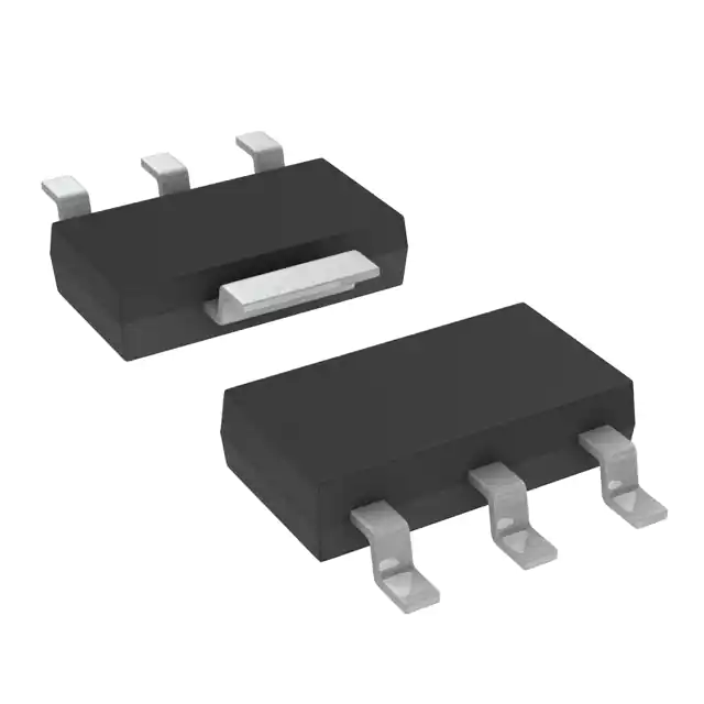
SOT−223
CASE 318E
STYLE 1
1
Device
Package
Shipping†
NSS1C201MZ4T1G
NSV1C201MZ4T1G
SOT−223
(Pb−Free)
1000/
Tape & Reel
NSS1C201MZ4T3G
SOT−223
(Pb−Free)
4000/
Tape & Reel
†For information on tape and reel specifications,
including part orientation and tape sizes, please
refer to our Tape and Reel Packaging Specification
Brochure, BRD8011/D.
Publication Order Number:
NSS1C201MZ4/D
�NSS1C201MZ4, NSV1C201MZ4
ELECTRICAL CHARACTERISTICS (TA = 25°C unless otherwise noted)
Characteristic
Symbol
Min
Typ
Max
Unit
Collector −Emitter Breakdown Voltage (IC = 10 mAdc, IB = 0)
V(BR)CEO
100
Vdc
Collector −Base Breakdown Voltage (IC = 0.1 mAdc, IE = 0)
V(BR)CBO
140
Vdc
Emitter −Base Breakdown Voltage (IE = 0.1 mAdc, IC = 0)
V(BR)EBO
7.0
Vdc
OFF CHARACTERISTICS
Collector Cutoff Current (VCB = 140 Vdc, IE = 0)
ICBO
100
nA
Emitter Cutoff Current (VEB = 6.0 Vdc)
IEBO
50
nA
ON CHARACTERISTICS
DC Current Gain (Note 4)
(IC = 10 mA, VCE = 2.0 V)
(IC = 500 mA, VCE = 2.0 V)
(IC = 1.0 A, VCE = 2.0 V)
(IC = 2.0 A, VCE = 2.0 V)
hFE
Collector −Emitter Saturation Voltage (Note 4)
(IC = 0.1 A, IB = 0.010 A)
(IC = 0.5 A, IB = 0.050 A)
(IC = 1.0 A, IB = 0.100 A)
(IC = 2.0 A, IB = 0.200 A)
VCE(sat)
Base −Emitter Saturation Voltage (Note 4)
(IC = 1.0 A, IB = 0.100 A)
VBE(sat)
Base −Emitter Turn−on Voltage (Note 4) (IC = 1.0 A, VCE = 2.0 V)
VBE(on)
Cutoff Frequency (IC = 100 mA, VCE = 5.0 V, f = 100 MHz)
150
120
80
40
360
V
0.030
0.060
0.100
0.180
V
1.10
0.850
V
fT
100
MHz
Input Capacitance (VEB = 0.5 V, f = 1.0 MHz)
Cibo
305
pF
Output Capacitance (VCB = 3.0 V, f = 1.0 MHz)
Cobo
22
pF
4. Pulsed Condition: Pulse Width = 300 msec, Duty Cycle ≤ 2%.
TYPICAL CHARACTERISTICS
PD, POWER DISSIPATION (W)
2.5
2.0
TC
1.5
1.0
TA
0.5
0
25
50
75
100
T, TEMPERATURE (°C)
Figure 1. Power Derating
http://onsemi.com
2
125
150
�NSS1C201MZ4, NSV1C201MZ4
TYPICAL CHARACTERISTICS
400
400
VCE = 2 V
150°C
320
360
hRE, DC CURRENT GAIN
hRE, DC CURRENT GAIN
360
280
240
25°C
200
160
120
−55°C
80
280
240
160
120
−55°C
80
40
0
0.001
0.01
0.1
1
0
0.001
10
0.1
1
IC, COLLECTOR CURRENT (A)
Figure 2. DC Current Gain
Figure 3. DC Current Gain
10
1
IC /IB = 20
VCE(sat), COLLECTOR−EMITTER
SATURATOIN VOLTAGE (V)
IC /IB = 10
0.1
150°C
25°C
0.1
150°C
25°C
0.01
0.001
0.01
−55°C
0.1
1
10
−55°C
0.01
0.001
IC, COLLECTOR CURRENT (A)
0.01
0.1
1
10
IC, COLLECTOR CURRENT (A)
Figure 4. Collector−Emitter Saturation Voltage
Figure 5. Collector−Emitter Saturation Voltage
1.4
1.4
IC /IB = 10
VBE(sat), BASE−EMITTER SATURATOIN VOLTAGE (V)
1.2
0.01
IC, COLLECTOR CURRENT (A)
1
VBE(sat), COLLECTOR−EMITTER
SATURATOIN VOLTAGE (V)
25°C
200
40
VBE(sat), BASE−EMITTER SATURATOIN VOLTAGE (V)
VCE = 4 V
150°C
320
1
150°C
0.8
0.6
25°C
0.4
−55°C
0.2
0
0.001
0.01
0.1
1
10
1.2
IC /IB = 50
−55°C
1
0.8
25°C
0.6
150°C
0.4
0.2
0
0.001
0.01
0.1
1
IC, COLLECTOR CURRENT (A)
IC, COLLECTOR CURRENT (A)
Figure 6. Base−Emitter Saturation Voltage
Figure 7. Base−Emitter Saturation Voltage
http://onsemi.com
3
10
�NSS1C201MZ4, NSV1C201MZ4
TYPICAL CHARACTERISTICS
1.00
VCE = 2 V
VCE(sat), COLLECTOR−EMITTER
SATURATOIN VOLTAGE (V)
VBE(on), BASE−EMITTER VOLTAGE
(V)
1.2
1.0
−55°C
0.8
25°C
0.6
150°C
0.4
0.2
0.0
0.001
0.01
0.1
1
0.5 A
1A
2A
0.10
TJ = 25°C
0.01
0.0001
10
0.001
IC, COLLECTOR CURRENT (A)
1
50
TJ = 25°C
fTEST = 1 MHz
350
COB, OUTPUT CAPACITANCE (pF)
CIB, INPUT CAPACITANCE (pF)
0.1
Figure 9. Collector Saturation Region
400
300
250
200
150
100
50
0
0
1
2
3
4
5
6
7
45
TJ = 25°C
fTEST = 1 MHz
40
35
30
25
20
15
10
5
0
0
8
10
20
30
40
50
60
70
80
90
100
VCB, COLLECTOR BASE VOLTAGE (V)
VEB, BASE−EMITTER VOLTAGE (V)
Figure 10. Input Capacitance
Figure 11. Output Capacitance
120
10
TJ = 25°C
fTEST = 1 MHz
VCE = 5 V
IC, COLLECTOR CURRENT (A)
fTau, CURRENT GAIN BANDWIDTH
(MHz)
0.01
IB, BASE CURRENT (A)
Figure 8. Base−Emitter Voltage
100
3A
IC = 0.1 A
80
60
40
20
0
0.001
0.01
0.1
1
10
0.5 mS
1
100 mS
1 mS
10 mS
0.1
TJ = 25°C
0.01
1
IC, COLLECTOR CURRENT (A)
10
VCE, COLLECTOR EMITTER VOLTAGE (V)
Figure 12. Current Gain Bandwidth Product
Figure 13. Safe Operating Area
http://onsemi.com
4
100
�MECHANICAL CASE OUTLINE
PACKAGE DIMENSIONS
SOT−223 (TO−261)
CASE 318E−04
ISSUE R
DATE 02 OCT 2018
SCALE 1:1
q
q
DOCUMENT NUMBER:
DESCRIPTION:
98ASB42680B
SOT−223 (TO−261)
Electronic versions are uncontrolled except when accessed directly from the Document Repository.
Printed versions are uncontrolled except when stamped “CONTROLLED COPY” in red.
PAGE 1 OF 2
ON Semiconductor and
are trademarks of Semiconductor Components Industries, LLC dba ON Semiconductor or its subsidiaries in the United States and/or other countries.
ON Semiconductor reserves the right to make changes without further notice to any products herein. ON Semiconductor makes no warranty, representation or guarantee regarding
the suitability of its products for any particular purpose, nor does ON Semiconductor assume any liability arising out of the application or use of any product or circuit, and specifically
disclaims any and all liability, including without limitation special, consequential or incidental damages. ON Semiconductor does not convey any license under its patent rights nor the
rights of others.
© Semiconductor Components Industries, LLC, 2018
www.onsemi.com
�SOT−223 (TO−261)
CASE 318E−04
ISSUE R
STYLE 1:
PIN 1.
2.
3.
4.
BASE
COLLECTOR
EMITTER
COLLECTOR
STYLE 2:
PIN 1.
2.
3.
4.
ANODE
CATHODE
NC
CATHODE
STYLE 6:
PIN 1.
2.
3.
4.
RETURN
INPUT
OUTPUT
INPUT
STYLE 7:
PIN 1.
2.
3.
4.
ANODE 1
CATHODE
ANODE 2
CATHODE
STYLE 11:
PIN 1. MT 1
2. MT 2
3. GATE
4. MT 2
STYLE 3:
PIN 1.
2.
3.
4.
GATE
DRAIN
SOURCE
DRAIN
STYLE 8:
STYLE 12:
PIN 1. INPUT
2. OUTPUT
3. NC
4. OUTPUT
CANCELLED
DATE 02 OCT 2018
STYLE 4:
PIN 1.
2.
3.
4.
SOURCE
DRAIN
GATE
DRAIN
STYLE 5:
PIN 1.
2.
3.
4.
STYLE 9:
PIN 1.
2.
3.
4.
INPUT
GROUND
LOGIC
GROUND
STYLE 10:
PIN 1. CATHODE
2. ANODE
3. GATE
4. ANODE
DRAIN
GATE
SOURCE
GATE
STYLE 13:
PIN 1. GATE
2. COLLECTOR
3. EMITTER
4. COLLECTOR
GENERIC
MARKING DIAGRAM*
AYW
XXXXXG
G
1
A
= Assembly Location
Y
= Year
W
= Work Week
XXXXX = Specific Device Code
G
= Pb−Free Package
(Note: Microdot may be in either location)
*This information is generic. Please refer to
device data sheet for actual part marking.
Pb−Free indicator, “G” or microdot “G”, may
or may not be present. Some products may
not follow the Generic Marking.
DOCUMENT NUMBER:
DESCRIPTION:
98ASB42680B
SOT−223 (TO−261)
Electronic versions are uncontrolled except when accessed directly from the Document Repository.
Printed versions are uncontrolled except when stamped “CONTROLLED COPY” in red.
PAGE 2 OF 2
ON Semiconductor and
are trademarks of Semiconductor Components Industries, LLC dba ON Semiconductor or its subsidiaries in the United States and/or other countries.
ON Semiconductor reserves the right to make changes without further notice to any products herein. ON Semiconductor makes no warranty, representation or guarantee regarding
the suitability of its products for any particular purpose, nor does ON Semiconductor assume any liability arising out of the application or use of any product or circuit, and specifically
disclaims any and all liability, including without limitation special, consequential or incidental damages. ON Semiconductor does not convey any license under its patent rights nor the
rights of others.
© Semiconductor Components Industries, LLC, 2018
www.onsemi.com
�onsemi,
, and other names, marks, and brands are registered and/or common law trademarks of Semiconductor Components Industries, LLC dba “onsemi” or its affiliates
and/or subsidiaries in the United States and/or other countries. onsemi owns the rights to a number of patents, trademarks, copyrights, trade secrets, and other intellectual property.
A listing of onsemi’s product/patent coverage may be accessed at www.onsemi.com/site/pdf/Patent−Marking.pdf. onsemi reserves the right to make changes at any time to any
products or information herein, without notice. The information herein is provided “as−is” and onsemi makes no warranty, representation or guarantee regarding the accuracy of the
information, product features, availability, functionality, or suitability of its products for any particular purpose, nor does onsemi assume any liability arising out of the application or use
of any product or circuit, and specifically disclaims any and all liability, including without limitation special, consequential or incidental damages. Buyer is responsible for its products
and applications using onsemi products, including compliance with all laws, regulations and safety requirements or standards, regardless of any support or applications information
provided by onsemi. “Typical” parameters which may be provided in onsemi data sheets and/or specifications can and do vary in different applications and actual performance may
vary over time. All operating parameters, including “Typicals” must be validated for each customer application by customer’s technical experts. onsemi does not convey any license
under any of its intellectual property rights nor the rights of others. onsemi products are not designed, intended, or authorized for use as a critical component in life support systems
or any FDA Class 3 medical devices or medical devices with a same or similar classification in a foreign jurisdiction or any devices intended for implantation in the human body. Should
Buyer purchase or use onsemi products for any such unintended or unauthorized application, Buyer shall indemnify and hold onsemi and its officers, employees, subsidiaries, affiliates,
and distributors harmless against all claims, costs, damages, and expenses, and reasonable attorney fees arising out of, directly or indirectly, any claim of personal injury or death
associated with such unintended or unauthorized use, even if such claim alleges that onsemi was negligent regarding the design or manufacture of the part. onsemi is an Equal
Opportunity/Affirmative Action Employer. This literature is subject to all applicable copyright laws and is not for resale in any manner.
PUBLICATION ORDERING INFORMATION
LITERATURE FULFILLMENT:
Email Requests to: orderlit@onsemi.com
onsemi Website: www.onsemi.com
◊
TECHNICAL SUPPORT
North American Technical Support:
Voice Mail: 1 800−282−9855 Toll Free USA/Canada
Phone: 011 421 33 790 2910
Europe, Middle East and Africa Technical Support:
Phone: 00421 33 790 2910
For additional information, please contact your local Sales Representative
�


 工商网监
湘ICP备2023018690号
工商网监
湘ICP备2023018690号
