FemtoClocks™
Crystal-to-LVCMOS/LVTTL Frequency
840001-34
DATASHEET
General Description
Features
The 840001-34 is a two output LVCMOS/LVTTL Synthesizer. One
output is the LVCMOS/LVTTL main synthesized clock output (Q)
and one output is a three-state LVCMOS/LVTTL reference clock
(REF_OUT) output at the frequency of the crystal oscillator. The
device can accept crystals from 15.3125MHz to 42.67MHz and
can synthesize outputs from 81.67MHz to 213.33MHz. The
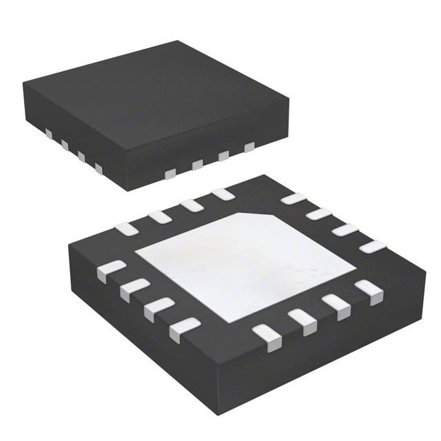
840001-34 is packaged in a 3mm x 3mm 16-pin VFQFN, making it
ideal for use on space constrained boards..
•
Two LVCMOS/LVTTL outputs, 22 typical output impedance
One main clock output (Q)
One three-state reference clock output (REF_OUT)
•
Crystal oscillator interface can accept crystals from
15.3125MHz to 42.67MHz, 18pF parallel resonant crystal
•
•
•
•
•
•
Q output frequency range: 81.67MHz to 213.33MHz
RMS phase jitter @106.25, (637kHz – 10MHz): 0.38ps (typical)
VCO range: 490MHz to 640MHz
Full 3.3V and 2.5V operating supply
0°C to 70°C ambient operating temperature
Available in lead-free (RoHS 6) package
Common Application Configuration Table
Inputs
Crystal (MHz)
M Divider
VCO (MHz)
N Divider
Output Frequency
(MHz)
40
15
600
6
100 (default)
26.5625
24
637.5
6
106.25
40
15
600
4
150
26.5625
24
637.5
3
212.5
25
25
625
5
125
25
25
625
4
156.25
10 Gigabit Ethernet
22.5
25
562.5
3
187.5
12 Gigabit Ethernet
19.44
32
622.08
4
155.52
SONET
Block Diagram
Serial Attached (SCSI),
PCI Express, Processor Clock
Fibre Channel
Serial ATA (SATA), Processor Clock
Fibre Channel 2
Ethernet
OE 1
VCO
490MHz - 640MHz
M-Div
11 = ÷15 (default)
10 = ÷24
01 = ÷25
00 = ÷32
M1
2
11 VDDO
XTAL_OUT 3
10 GND
XTAL_IN
Q
M0 4
9 VDD
5
6
7
8
N1
XTAL_OUT
Phase
Detector
N0
OSC
16 15 14 13
12 Q
nc
XTAL_IN
N-Div
00 = ÷3
01 = ÷4
10 = ÷5
11 = ÷6 (default)
nc
VDDA
REF_OUT
nc
(Pullup)
REF_OUT
Pin Assignment
M1
OE
Application
840001-34
16 Lead VFQFN
3mm x 3mm x 0.95 package body
K Package
Top View
(Pullup)
M0 (Pullup)
N1 (Pullup)
N0 (Pullup)
840001-34 Rev A 3/30/15
1
©2015 Integrated Device Technology, Inc.
�840001-34 DATASHEET
Table 1. Pin Descriptions
Number
Name
Type
1
OE
Input
2,
3
XTAL_IN,
XTAL_OUT
Input
Description
Pullup
Output enable pin. When HIGH, REF_OUT output is enabled. When LOW,
forces REF_OUT to Hi-Z state. See Table 3A. LVCMOS/LVTTL interface levels.
Crystal oscillator interface. XTAL_IN is the input. XTAL_OUT is the output.
4, 5
M0, M1
Input
6, 14, 15
nc
Unused
Pullup
M divider inputs. LVCMOS/LVTTL interface levels. See Table 3B.
7, 8
N0, N1
Input
9
VDD
Power
Core supply pin.
10
GND
Power
Power supply ground.
11
VDDO
Power
Output supply pin.
12
Q
Output
Single-ended clock output. 22 typical output impedance.
LVCMOS/LVTTL interface levels.
13
REF_OUT
Output
Single-ended three-state reference clock output. 22 typical output impedance.
LVCMOS/LVTTL interface levels.
16
VDDA
Power
Analog supply pin.
No connect.
Pullup
Determines output divider value as defined in Table 3C.
LVCMOS/LVTTL interface levels.
NOTE: Pullup refers to intenal input resistors. See Table 2, Pin Characteristics, for typical values.
Table 2. Pin Characteristics
Symbol
Parameter
CIN
Input Capacitance
CPD
Power Dissipation Capacitance
RPULLUP
Input Pullup Resistor
ROUT
Output Impedance
Rev A 3/30/15
Test Conditions
Minimum
Typical
Maximum
Units
4
pF
VDD, VDDO = 3.465V
8
pF
VDD, VDDO = 2.625V
6
pF
51
k
VDD, VDDO = 3.3V±5%
14
22
30
VDD, VDDO = 2.5V±5%
16
26
36
2
FEMTOCLOCKS™ CRYSTAL-TO-LVCMOS/LVTTL FREQUENCY
SYNTHESIZER
�840001-34 DATASHEET
Table 3A. Control Input Function Table
Control Input
Output
OE
REF_OUT
0
Hi-Z
1
Active (default)
Table 3B. M Divider Function Table
Control Inputs
M1
M0
Feedback Divider Ratio
0
0
÷32
0
1
÷25
1
0
÷24
1
1
÷15 (default)
Table 3C. N Divider Function Table
Control Inputs
N1
N0
Output Divider Ratio
0
0
÷3
0
1
÷4
1
0
÷5
1
1
÷6 (default)
Rev A 3/30/15
3
FEMTOCLOCKS™ CRYSTAL-TO-LVCMOS/LVTTL FREQUENCY
SYNTHESIZER
�840001-34 DATASHEET
Absolute Maximum Ratings
NOTE: Stresses beyond those listed under Absolute Maximum Ratings may cause permanent damage to the device. These ratings are stress
specifications only. Functional operation of product at these conditions or any conditions beyond those listed in the DC Characteristics or AC
Characterisitcs is not implied. Exposure to absolute maximum rating conditions for extended periods may affect product reliability.
Item
Rating
Supply Voltage, VDD
4.6V
Inputs, VI
-0.5V to VDD + 0.5V
Outputs,VO
-0.5V to VDD + 0.5V
Package Thermal Impedance, JA
76.1C/W (0 mps)
Storage Temperature, TSTG
-65C to 150C
DC Electrical Characteristics
Table 4A. Power Supply DC Characteristics, VDD = VDDO = 3.3V ± 5%, TA = 0°C to 70°C
Symbol
Parameter
VDD
Test Conditions
Minimum
Typical
Maximum
Units
Positive Supply Voltage
3.135
3.3
3.465
V
VDDA
Analog Supply Voltage
VDD – 0.12
3.3
VDD
V
VDDO
Output Supply Voltage
3.135
3.3
3.465
V
IDD
Power Supply Current
100
mA
IDDA
Analog Supply Current
12
mA
IDDO
Output Supply Current
35
mA
Table 4B. Power Supply DC Characteristics, VDD = VDDO = 2.5V ± 5%, TA = 0°C to 70°C
Symbol
Parameter
VDD
Minimum
Typical
Maximum
Units
Positive Supply Voltage
2.375
2.5
2.625
V
VDDA
Analog Supply Voltage
VDD – 0.12
3.3
VDD
V
VDDO
Output Supply Voltage
2.375
2.5
2.625
V
IDD
Power Supply Current
90
mA
IDDA
Analog Supply Current
12
mA
IDDO
Output Supply Current
25
mA
Rev A 3/30/15
Test Conditions
4
FEMTOCLOCKS™ CRYSTAL-TO-LVCMOS/LVTTL FREQUENCY
SYNTHESIZER
�840001-34 DATASHEET
Table 4C. LVCMOS/LVTTL DC Characteristics, VDD = VDDO = 3.3V ± 5% or 2.5V ± 5%, TA = 0°C to 70°CC
Symbol
Parameter
Test Conditions
Minimum
VDD = 3.3V
Typical
Maximum
Units
VIH
Input High Voltage
2
VDD + 0.3
V
VDD = 2.5V
1.7
VDD + 0.3
V
VIL
Input Low Voltage
VDD = 3.3V
-0.3
0.8
V
VDD = 2.5V
-0.3
0.7
V
IIH
Input High
Current
OE, M0, M1,
N0, N1
VDD = VIN = 3.465V or 2.625V
5
µA
IIL
Input Low
Current
OE, M0, M1,
N0, N1
VDD = VIN = 3.465V or 2.625V
-150
µA
V
Output High Voltage; NOTE 1
VDDO = 3.3V±5%
2.6
VOH
VDDO = 2.5V±5%
1.8
V
VOL
Output Low Voltage; NOTE 1
VDDO = 3.3V±5% or 2.5V±5%
0.5
V
NOTE 1: Outputs terminated with 50 to VDDO/2. See Parameter Measurement Information, Output Load Test Circuit diagrams.
Table 5. Crystal Characteristics
Parameter
Test Conditions
Minimum
Maximum
Units
42.67
MHz
Equivalent Series Resistance (ESR)
50
Shunt Capacitance
7
pF
Drive Level
1
mW
Mode of Oscillation
Typical
Fundamental
Frequency
15.3125
NOTE: It is not recommended to overdrive the crystal input with an external clock.
Rev A 3/30/15
5
FEMTOCLOCKS™ CRYSTAL-TO-LVCMOS/LVTTL FREQUENCY
SYNTHESIZER
�840001-34 DATASHEET
AC Electrical Characteristics
Table 6A. AC Characteristics, VDD = VDDO = 3.3V ± 5%, TA = 0°C to 70°C
Parameter
Symbol
fOUT
Output Frequency
tjit(Ø)
tR / tF
odc
RMS Phase Jitter, Random;
NOTE 1
Output Rise/Fall Time
Output Duty Cycle
Test Conditions
Minimum
Typical
81.67
Maximum
Units
213.33
MHz
100MHz, Integration Range:
637kHz – 10MHz
0.54
ps
106.25MHz, Integration Range:
637kHz – 10MHz
0.38
ps
20% to 80%
200
700
ps
Q, N = 3
40
60
%
Q, N 3
48
52
%
REF_OUT
48
52
%
NOTE: Electrical parameters are guaranteed over the specified ambient operating temperature range, which is established when device is
mounted in a test socket with maintained transverse airflow greater than 500 lfpm. Device will meet specifications after thermal equilibrium has
been reached under these conditions
NOTE 1: Please refer to Phase Noise Plot.
Table 6B. AC Characteristics, VDD = VDDO = 2.5V ± 5%, TA = 0°C to 70°C
Parameter
Symbol
fOUT
Output Frequency
tjit(Ø)
RMS Phase Jitter, Random;
NOTE 1
tR / tF
odc
Output Rise/Fall Time
Output Duty Cycle
Test Conditions
Minimum
Typical
81.67
Maximum
Units
213.33
MHz
100MHz, Integration Range:
637kHz – 10MHz
0.54
ps
106.25MHz, Integration Range:
637kHz – 10MHz
0.38
ps
20% to 80%
300
800
ps
Q, N = 3
35
65
%
Q, N 3
40
60
%
REF_OUT
45
55
%
NOTE: Electrical parameters are guaranteed over the specified ambient operating temperature range, which is established when device is
mounted in a test socket with maintained transverse airflow greater than 500 lfpm. Device will meet specifications after thermal equilibrium has
been reached under these conditions
NOTE 1: Please refer to Phase Noise Plot.
Rev A 3/30/15
6
FEMTOCLOCKS™ CRYSTAL-TO-LVCMOS/LVTTL FREQUENCY
SYNTHESIZER
�840001-34 DATASHEET
➝
Typical Phase Noise at 100MHz (3.3V)
Filter
Raw Phase Noise Data
➝
➝
Noise Power
dBc
Hz
100MHz
RMS Phase Jitter (Random)
637kHz to 10MHz = 0.54ps (typical)
Phase Noise Result by adding
a filter to raw data
Offset Frequency (Hz)
➝
Typical Phase Noise at 106.25MHz (3.3V)
Fibre Channel Filter
Raw Phase Noise Data
➝
➝
Noise Power
dBc
Hz
106.25MHz
RMS Phase Jitter (Random)
637kHz to 10MHz = 0.38ps (typical)
Phase Noise Result by adding a
Fibre Channel filter to raw data
Offset Frequency (Hz)
Rev A 3/30/15
7
FEMTOCLOCKS™ CRYSTAL-TO-LVCMOS/LVTTL FREQUENCY
SYNTHESIZER
�840001-34 DATASHEET
Parameter Measurement Information
1.25V±5%
1.65V±5%
1.25V±5%
1.65V±5%
SCOPE
VDD,
VDDO
VDDA
SCOPE
VDD,
VDDO
VDDA
Qx
GND
GND
-1.65V±5%
-1.25V±5%
3.3V LVCMOS Output Load AC Test Circuit
Qx
2.5V LVCMOS Output Load AC Test Circuit
Phase Noise Plot
V
DDO
Noise Power
Q,
REF_OUT
2
t PW
Phase Noise Mask
f1
Offset Frequency
t
odc =
f2
PERIOD
t PW
x 100%
t PERIOD
RMS Jitter = Area Under the Masked Phase Noise Plot
RMS Phase Jitter
Q, REF_OUT
Output Duty Cycle/Pulse Width/Period
80%
80%
tR
tF
20%
20%
Output Rise/Fall Time
Rev A 3/30/15
8
FEMTOCLOCKS™ CRYSTAL-TO-LVCMOS/LVTTL FREQUENCY
SYNTHESIZER
�840001-34 DATASHEET
Application Information
Power Supply Filtering Technique
3.3V
To achieve optimum jitter performance, power supply isolation is
required. The ICS40001I-34 provides separate power supplies to
isolate any high switching noise from the outputs to the internal
PLL. VDD, VDDA, and VDDO should be individually connected to the
power supply plane through vias, and 0.01µF bypass capacitors
should be used for each pin. Figure 1 illustrates this for a generic
VDD pin and also shows that VDDA requires that an additional 10
resistor along with a 10F bypass capacitor be connected to the
VDDA pin.
VDD
.01µF
10Ω
.01µF
10µF
VDDA
Figure 1. Power Supply Filtering
Recommendations for Unused Input and Output Pins
Inputs:
Outputs:
LVCMOS Control Pins:
LVCMOS Output
All control pins have internal pull-ups; additional resistance is not
required but can be added for additional protection. A 1k resistor
can be used.
All unused LVCMOS output can be left floating. There should be no
trace attached.
Crystal Input Interface
The ICS840001I-34 has been characterized with 18pF parallel
resonant crystals. The capacitor values, C1 and C2, shown in
Figure 2 below were determined using a 26.5625MHz, 18pF
parallel resonant crystal and were chosen to minimize the ppm
error. The optimum C1 and C2 values can be slightly adjusted for
different board layouts.
XTAL_IN
C1
33pF
X1
18pF Parallel Crystal
XTAL_OUT
C2
33pF
Figure 2. Crystal Input Interface
Rev A 3/30/15
9
FEMTOCLOCKS™ CRYSTAL-TO-LVCMOS/LVTTL FREQUENCY
SYNTHESIZER
�840001-34 DATASHEET
VFQFN EPAD Thermal Release Path
In order to maximize both the removal of heat from the package
and the electrical performance, a land pattern must be
incorporated on the Printed Circuit Board (PCB) within the footprint
of the package corresponding to the exposed metal pad or
exposed heat slug on the package, as shown in Figure 4. The
solderable area on the PCB, as defined by the solder mask, should
be at least the same size/shape as the exposed pad/slug area on
the package to maximize the thermal/electrical performance.
Sufficient clearance should be designed on the PCB between the
outer edges of the land pattern and the inner edges of pad pattern
for the leads to avoid any shorts.
application specific and dependent upon the package power
dissipation as well as electrical conductivity requirements. Thus,
thermal and electrical analysis and/or testing are recommended to
determine the minimum number needed. Maximum thermal and
electrical performance is achieved when an array of vias is
incorporated in the land pattern. It is recommended to use as many
vias connected to ground as possible. It is also recommended that
the via diameter should be 12 to 13mils (0.30 to 0.33mm) with 1oz
copper via barrel plating. This is desirable to avoid any solder
wicking inside the via during the soldering process which may
result in voids in solder between the exposed pad/slug and the
thermal land. Precautions should be taken to eliminate any solder
voids between the exposed heat slug and the land pattern. Note:
These recommendations are to be used as a guideline only. For
further information, please refer to the Application Note on the
Surface Mount Assembly of Amkor’s Thermally/Electrically
Enhance Leadframe Base Package, Amkor Technology.
While the land pattern on the PCB provides a means of heat
transfer and electrical grounding from the package to the board
through a solder joint, thermal vias are necessary to effectively
conduct from the surface of the PCB to the ground plane(s). The
land pattern must be connected to ground through these vias. The
vias act as “heat pipes”. The number of vias (i.e. “heat pipes”) are
PIN
PIN PAD
SOLDER
EXPOSED HEAT SLUG
GROUND PLANE
THERMAL VIA
SOLDER
LAND PATTERN
(GROUND PAD)
PIN
PIN PAD
Figure 4. P.C. Assembly for Exposed Pad Thermal Release Path – Side View (drawing not to scale)
Rev A 3/30/15
10
FEMTOCLOCKS™ CRYSTAL-TO-LVCMOS/LVTTL FREQUENCY
SYNTHESIZER
�840001-34 DATASHEET
Reliability Information
Table 7. JA vs. Air Flow Table for a 16 Lead VFQFN
JA at 0 Air Flow
Meters per Second
Multi-Layer PCB, JEDEC Standard Test
Boards
0
1
2.5
76.1°C/W
66.5
59.7
Transistor Count
The transistor count for 840001-34 is: 2805
Rev A 3/30/15
11
FEMTOCLOCKS™ CRYSTAL-TO-LVCMOS/LVTTL FREQUENCY
SYNTHESIZER
�840001-34 DATASHEET
Package Outline and Package Dimensions
Package Outline - K Suffix for 16 Lead VFQFN
(Ref.)
Seating Plane
ND & NE
Even
(ND-1)x e
(R ef.)
A1
Index Area
A3
N
Top View
Anvil
Singulation
or
Sawn
Singulation
L
N
e (Typ.)
2 If ND & NE
1
are Even
2
E2
(NE -1)x e
(Re f.)
E2
2
b
A
(Ref.)
D
Chamfer 4x
0.6 x 0.6 max
OPTIONAL
e
ND & NE
Odd
0. 08
C
D2
2
Thermal
Base
D2
C
Table 8. Package Dimensions
Symbol
N
A
A1
A3
b
ND & NE
D&E
D2 & E2
e
L
JEDEC Variation: VEED-2/-4
All Dimensions in Millimeters
Minimum
Maximum
16
0.80
1.00
0
0.05
0.25 Ref.
0.18
0.30
4
3.00 Basic
1.00
1.80
0.50 Basic
0.30
0.50
Reference Document: JEDEC Publication 95, MO-220
Rev A 3/30/15
12
FEMTOCLOCKS™ CRYSTAL-TO-LVCMOS/LVTTL FREQUENCY
SYNTHESIZER
�840001-34 DATASHEET
Ordering Information
Table 9. Ordering Information
Part/Order Number
ICS840001AK-34LF
ICS840001AK-34LFT
Marking
A34L
A34L
Package
“Lead-Free” 16 Lead VFQFN
“Lead-Free” 16 Lead VFQFN
Shipping Packaging
Tray
Tape & Reel
Temperature
0°C to 70°C
0°C to 70°C
NOTE: Parts that are ordered with an "LF" suffix to the part number are the Pb-Free configuration and are RoHS compliant.
Rev A 3/30/15
13
FEMTOCLOCKS™ CRYSTAL-TO-LVCMOS/LVTTL FREQUENCY
SYNTHESIZER
�840001-34 DATASHEET
Revision History Sheet
Rev
Table
A
Rev A 3/30/15
Description of Change
Date
11
13
Updated VFQFN EPAD Thermal Release Path section.
Updated Package Drawing.
10/27/08
Deleted HiPerClockS references.
Crystal Characteristics Table - added note.
Deleted application note, LVCMOS to XTAL Interface.
Deleted quantity from tape and reel
11/2/12
T9
1
5
9
13
T9
13
Ordering Information - removed leaded devices.
Updated data sheet format.
3/30/15
A
A
Page
T5
14
FEMTOCLOCKS™ CRYSTAL-TO-LVCMOS/LVTTL FREQUENCY
SYNTHESIZER
�Corporate Headquarters
Sales
Tech Support
6024 Silver Creek Valley Road
San Jose, CA 95138 USA
1-800-345-7015 or 408-284-8200
Fax: 408-284-2775
www.IDT.com
email: clocks@idt.com
DISCLAIMER Integrated Device Technology, Inc. (IDT) and its subsidiaries reserve the right to modify the products and/or specifications described herein at any time and at IDT’s sole discretion. All information in
this document, including descriptions of product features and performance, is subject to change without notice. Performance specifications and the operating parameters of the described products are determined
in the independent state and are not guaranteed to perform the same way when installed in customer products. The information contained herein is provided without representation or warranty of any kind, whether
express or implied, including, but not limited to, the suitability of IDT’s products for any particular purpose, an implied warranty of merchantability, or non-infringement of the intellectual property rights of others. This
document is presented only as a guide and does not convey any license under intellectual property rights of IDT or any third parties.
IDT’s products are not intended for use in applications involving extreme environmental conditions or in life support systems or similar devices where the failure or malfunction of an IDT product can be reasonably
expected to significantly affect the health or safety of users. Anyone using an IDT product in such a manner does so at their own risk, absent an express, written agreement by IDT.
While the information presented herein has been checked for both accuracy and reliability, Integrated Device Technology (IDT) assumes no responsibility for either its use or for the infringement of any patents or
other rights of third parties, which would result from its use. No other circuits, patents, or licenses are implied. This product is intended for use in normal commercial applications. Any other applications, such as
those requiring extended temperature ranges, high reliability or other extraordinary environmental requirements are not recommended without additional processing by IDT. IDT reserves the right to change any
circuitry or specifications without notice. IDT does not authorize or warrant any IDT product for use in life support devices or critical medical instruments.
Integrated Device Technology, IDT and the IDT logo are registered trademarks of IDT. Product specification subject to change without notice. Other trademarks and service marks used herein, including protected
names, logos and designs, are the property of IDT or their respective third party owners.
Copyright ©2015 Integrated Device Technology, Inc.. All rights reserved.
�IMPORTANT NOTICE AND DISCLAIMER
RENESAS ELECTRONICS CORPORATION AND ITS SUBSIDIARIES (“RENESAS”) PROVIDES TECHNICAL
SPECIFICATIONS AND RELIABILITY DATA (INCLUDING DATASHEETS), DESIGN RESOURCES (INCLUDING
REFERENCE DESIGNS), APPLICATION OR OTHER DESIGN ADVICE, WEB TOOLS, SAFETY INFORMATION, AND
OTHER RESOURCES “AS IS” AND WITH ALL FAULTS, AND DISCLAIMS ALL WARRANTIES, EXPRESS OR IMPLIED,
INCLUDING, WITHOUT LIMITATION, ANY IMPLIED WARRANTIES OF MERCHANTABILITY, FITNESS FOR A
PARTICULAR PURPOSE, OR NON-INFRINGEMENT OF THIRD PARTY INTELLECTUAL PROPERTY RIGHTS.
These resources are intended for developers skilled in the art designing with Renesas products. You are solely responsible
for (1) selecting the appropriate products for your application, (2) designing, validating, and testing your application, and (3)
ensuring your application meets applicable standards, and any other safety, security, or other requirements. These
resources are subject to change without notice. Renesas grants you permission to use these resources only for
development of an application that uses Renesas products. Other reproduction or use of these resources is strictly
prohibited. No license is granted to any other Renesas intellectual property or to any third party intellectual property.
Renesas disclaims responsibility for, and you will fully indemnify Renesas and its representatives against, any claims,
damages, costs, losses, or liabilities arising out of your use of these resources. Renesas' products are provided only subject
to Renesas' Terms and Conditions of Sale or other applicable terms agreed to in writing. No use of any Renesas resources
expands or otherwise alters any applicable warranties or warranty disclaimers for these products.
(Rev.1.0 Mar 2020)
Corporate Headquarters
Contact Information
TOYOSU FORESIA, 3-2-24 Toyosu,
Koto-ku, Tokyo 135-0061, Japan
www.renesas.com
For further information on a product, technology, the most
up-to-date version of a document, or your nearest sales
office, please visit:
www.renesas.com/contact/
Trademarks
Renesas and the Renesas logo are trademarks of Renesas
Electronics Corporation. All trademarks and registered
trademarks are the property of their respective owners.
© 2020 Renesas Electronics Corporation. All rights reserved.
�


 工商网监
湘ICP备2023018690号
工商网监
湘ICP备2023018690号
