FemtoClock® Crystal-to-LVDS Frequency
Synthesizer w/Integrated Fanout Buffer
ICS844256D
DATA SHEET
General Description
Features
The ICS844256D is a Crystal-to-LVDS Clock Synthesizer/Fanout
Buffer designed for SONET and Gigabit Ethernet applications. The
output frequency can be set using the frequency select pins and a
25MHz crystal for Ethernet frequencies, or a 19.44MHz crystal for
SONET. The low phase noise characteristics of the ICS844256D
make it an ideal clock for these demanding applications.
•
•
•
•
•
Six differential LVDS output pairs
•
•
•
Full 3.3V or mixed 3.3V core, 2.5V output supply mode
0°C to 70°C ambient operating temperature
Crystal oscillator interface
Output frequency range: 62.5MHz - 625MHz
Crystal input frequency range:15.625MHz - 25.5MHz
RMS phase jitter @ 125MHz, using a 25MHz crystal
(1.875MHz – 20MHz): 0.43ps (typical)
Available in lead-free (RoHS 6) package
Divider Function Table
Inputs
Function
FB_SEL
N_SEL1
N_SEL0
M Divider Value
N Divider Value
M/N Divider Value
0
0
0
25
1
25
0
0
1
25
2
12.5
0
1
0
25
4
6.25
0
1
1
25 (default)
5
5
1
0
0
32
1
32
1
0
1
32
2
16
1
1
0
32
4
8
1
1
1
32
8
4
Pin Assignment
Block Diagram
Q0
PLL_BYPASS Pullup
nQ0
Q1
1
XTAL_IN
OSC
PLL
0
N
Output
Divider
nQ1
Q2
nQ2
XTAL_OUT
Q3
nQ3
M
Feedback
Divider
FB_SEL Pulldown
N_SEL1
N_SEL0
Pullup
ICS844256DG REVISION A AUGUST 5, 2010
24
23
22
21
20
19
18
17
16
15
14
13
Q3
nQ3
Q4
nQ4
Q5
nQ5
N_SEL1
GND
GND
N_SEL0
XTAL_OUT
XTAL_IN
ICS844256D
nQ4
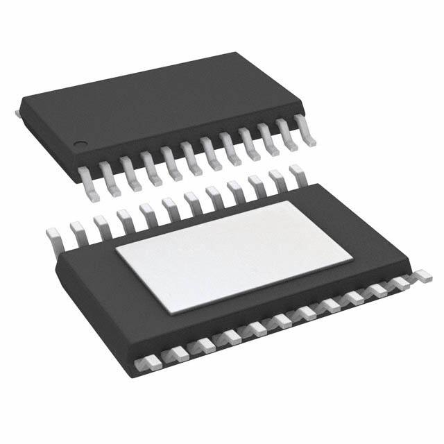
24-Lead TSSOP, E-Pad
4.40mm x 7.8mm x 0.925mm
package body
G Package
Top View
nQ5
1
1
2
3
4
5
6
7
8
9
10
11
12
Q4
Q5
Pullup
VDDO
VDDO
nQ2
Q2
nQ1
Q1
nQ0
Q0
PLL_BYPASS
VDDA
VDD
FB_SEL
©2010 Integrated Device Technology, Inc.
�FEMTOCLOCK® CRYSTAL-TO-LVDS FREQUENCY SYNTHESIZER W/INTEGRATED FANOUT BUFFER
ICS844256D Data Sheet
Table 1. Pin Descriptions
Number
Name
1, 2
VDDO
Power
Type
Output supply pins.
Description
3, 4
nQ2, Q2
Output
Differential output pair. LVDS interface levels.
5, 6
nQ1, Q1
Output
Differential output pair. LVDS interface levels.
7, 8
nQ0, Q0
Output
Differential output pair. LVDS interface levels.
9
PLL_BYPASS
Input
10
VDDA
Power
Analog supply pin.
11
VDD
Power
Core supply pin.
12
FB_SEL
Input
13,
14
XTAL_IN,
XTAL_OUT
Input
15,
18
N_SEL0,
N_SEL1
Input
Pullup
Pulldown
PLL Bypass. When LOW, the output is driven from the VCO output. When HIGH,
the PLL is bypassed and the output frequency = crystal frequency ÷ N output
divider. LVCMOS / LVTTL interface levels.
Feedback and output frequency select pin. LVCMOS/LVTTL interface levels.
See Table 3.
Crystal oscillator interface. XTAL_IN is the input. XTAL_OUT is the output.
Pullup
Feedback and output frequency select pins. LVCMOS/LVTTL interface levels.
See Table 3.
16, 17
GND
Power
Power supply ground.
19, 20
nQ5, Q5
Output
Differential output pair. LVDS interface levels.
21, 22
nQ4, Q4
Output
Differential output pair. LVDS interface levels.
23, 24
nQ3, Q3
Output
Differential output pair. LVDS interface levels.
NOTE: Pullup and Pulldown refer to internal input resistors. See Table 2, Pin Characteristics, for typical values.
Table 2. Pin Characteristics
Symbol
Parameter
CIN
Input Capacitance
4
pF
RPULLUP
Input Pullup Resistor
51
kΩ
RPULLDOWN
Input Pulldown Resistor
51
kΩ
ICS844256DG REVISION A AUGUST 5, 2010
Test Conditions
2
Minimum
Typical
Maximum
Units
©2010 Integrated Device Technology, Inc.
�FEMTOCLOCK® CRYSTAL-TO-LVDS FREQUENCY SYNTHESIZER W/INTEGRATED FANOUT BUFFER
ICS844256D Data Sheet
Function Tables
Table 3. Example Frequency Function Table
Inputs
Function
XTAL (MHz)
FB_SEL
N_SEL1
N_SEL0
M Divider Value
VCO (MHz)
N Divider Value
Output (MHz)
20
0
0
0
25
500
1
500
20
0
0
1
25
500
2
250
20
0
1
0
25
500
4
125
20
0
1
1
25
500
5
100
21.25
0
1
1
25
531.25
5
106.25
24
0
0
0
25
600
1
600
24
0
0
1
25
600
2
300
24
0
1
0
25
600
4
150
24
0
1
1
25
600
5
120
25
0
0
0
25
625
1
625
25
0
0
1
25
625
2
312.5
25
0
1
0
25
625
4
156.25
25
0
1
1
25
625
5
125
25.5
0
1
0
25
637.5
4
159.375
15.625
1
1
1
32
500
8
62.5
18.5625
1
1
1
32
594
8
74.25
18.75
1
0
0
32
600
1
600
18.75
1
0
1
32
600
2
300
18.75
1
1
0
32
600
4
150
18.75
1
1
1
32
600
8
75
19.44
1
0
0
32
622.08
1
622.08
19.44
1
0
1
32
622.08
2
311.04
19.44
1
1
0
32
622.08
4
155.52
19.44
1
1
1
32
622.08
8
77.76
19.53125
1
0
0
32
625
1
625
19.53125
1
0
1
32
625
2
312.5
19.53125
1
1
0
32
625
4
156.25
19.53125
1
1
1
32
625
8
78.125
20
1
1
1
32
640
8
80
ICS844256DG REVISION A AUGUST 5, 2010
3
©2010 Integrated Device Technology, Inc.
�ICS844256D Data Sheet
FEMTOCLOCK® CRYSTAL-TO-LVDS FREQUENCY SYNTHESIZER W/INTEGRATED FANOUT BUFFER
Absolute Maximum Ratings
NOTE: Stresses beyond those listed under Absolute Maximum Ratings may cause permanent damage to the device.
These ratings are stress specifications only. Functional operation of product at these conditions or any conditions beyond
those listed in the DC Characteristics or AC Characteristics is not implied. Exposure to absolute maximum rating conditions for
extended periods may affect product reliability.
Item
Rating
Supply Voltage, VDD
4.6V
Inputs, VI
XTAL_IN
Other Inputs
0V to VDD
-0.5V to VDD + 0.5V
Outputs, IO
Continuous Current
Surge Current
10mA
15mA
Package Thermal Impedance, θJA
32.1°C/W (0 mps)
Storage Temperature, TSTG
-65°C to 150°C
DC Electrical Characteristics
Table 4A. Power Supply DC Characteristics, VDD = VDDO = 3.3V ± 5%, TA = 0°C to 70°C
Symbol
Parameter
VDD
Test Conditions
Minimum
Typical
Maximum
Units
Positive Supply Voltage
3.135
3.3
3.465
V
VDDA
Analog Supply Voltage
VDD – 0.11
3.3
VDD
V
VDDO
Output Supply Voltage
3.135
3.3
3.465
V
IDD
Power Supply Current
172
mA
IDDA
Analog Supply Current
11
mA
IDDO
Output Supply Current
72
mA
Table 4B. Power Supply DC Characteristics, VDD = 3.3V ± 5%, VDDO = 2.5V ± 5%, TA = 0°C to 70°C
Symbol
Parameter
VDD
Minimum
Typical
Maximum
Units
Positive Supply Voltage
3.135
3.3
3.465
V
VDDA
Analog Supply Voltage
VDD – 0.11
3.3
VDD
V
VDDO
Output Supply Voltage
2.375
2.5
2.625
V
IDD
Power Supply Current
172
mA
IDDA
Analog Supply Current
11
mA
IDDO
Output Supply Current
70
mA
ICS844256DG REVISION A AUGUST 5, 2010
Test Conditions
4
©2010 Integrated Device Technology, Inc.
�FEMTOCLOCK® CRYSTAL-TO-LVDS FREQUENCY SYNTHESIZER W/INTEGRATED FANOUT BUFFER
ICS844256D Data Sheet
Table 4C. LVCMOS/LVTTL DC Characteristics, VDD = 3.3V ± 5%, VDDO = 3.3V ± 5% or 2.5V ± 5%, TA = 0°C to 70°C
Symbol
Parameter
VIH
Input High Voltage
VIL
Input Low Voltage
IIH
Input High Current
IIL
Input Low Current
Test Conditions
Minimum
Typical
Maximum
Units
2
VDD + 0.3
V
-0.3
0.8
V
FB_SEL
VDD = VIN = 3.465V
150
µA
PLL_BYPASS,
N_SEL0, N_SEL1
VDD = VIN = 3.465V
5
µA
FB_SEL
VDD = 3.465V, VIN = 0V
-5
µA
PLL_BYPASS,
N_SEL0, N_SEL1
VDD = 3.465V, VIN = 0V
-150
µA
Table 4D. LVDS DC Characteristics, VDD = VDDO = 3.3V ± 5%, TA = 0°C to 70°C
Symbol
Parameter
VOD
Differential Output Voltage
∆VOD
VOD Magnitude Change
VOS
Offset Voltage
∆VOS
VOS Magnitude Change
Test Conditions
Minimum
Typical
Maximum
Units
247
350
454
mV
50
mV
1.45
V
50
mV
1.125
1.25
Table 4E. LVDS DC Characteristics, VDD = 3.3V ± 5%, VDDO = 2.5V ± 5%, TA = 0°C to 70°C
Symbol
Parameter
VOD
Differential Output Voltage
∆VOD
VOD Magnitude Change
VOS
Offset Voltage
∆VOS
VOS Magnitude Change
Test Conditions
Minimum
Typical
Maximum
Units
247
350
454
mV
50
mV
1.45
V
50
mV
1.125
1.25
Table 5. Crystal Characteristics
Parameter
Test Conditions
Minimum
Maximum
Units
25.5
MHz
Equivalent Series Resistance (ESR)
50
Ω
Shunt Capacitance
7
pF
Drive Level
1
mW
Mode of Oscillation
Typical
Fundamental
Frequency
15.625
NOTE: Characterized using an 18pF parallel resonant crystal.
ICS844256DG REVISION A AUGUST 5, 2010
5
©2010 Integrated Device Technology, Inc.
�ICS844256D Data Sheet
FEMTOCLOCK® CRYSTAL-TO-LVDS FREQUENCY SYNTHESIZER W/INTEGRATED FANOUT BUFFER
AC Electrical Characteristics
Table 6A. AC Characteristics, VDD = VDDO = 3.3V ± 5%, TA = 0°C to 70°C
Symbol
Parameter
fOUT
Output Frequency
tsk(o)
Output Skew; NOTE 1, 2
tjit(Ø)
RMS Phase Jitter (Random);
NOTE 3
tR / tF
Output Rise/Fall Time
odc
Output Duty Cycle
tLOCK
PLL Lock Time
Test Conditions
Minimum
Typical
62.5
125MHz (1.875MHz – 20MHz)
20% to 80%
Maximum
Units
625
MHz
65
ps
0.43
200
ps
565
ps
≤ 312.5MHz
47
53
%
> 312.5MHz
45
55
%
25
ms
NOTE: Electrical parameters are guaranteed over the specified ambient operating temperature range, which is established when the device is
mounted in a test socket with maintained transverse airflow greater than 500 lfpm. The device will meet specifications after thermal equilibrium
has been reached under these conditions.
NOTE 1: Defined as skew between outputs at the same supply voltage and with equal load conditions. Measured at the output differential
cross points.
NOTE 2: This parameter is defined in accordance with JEDEC Standard 65.
NOTE 3: Refer to the Phase Noise Plot.
Table 6B. AC Characteristics, VDD = 3.3V ± 5%, VDDO = 2.5V ± 5%, TA = 0°C to 70°C
Symbol
Parameter
fOUT
Output Frequency
tsk(o)
Output Skew; NOTE 1, 2
tjit(Ø)
RMS Phase Jitter (Random);
NOTE 3
tR / tF
Output Rise/Fall Time
odc
Output Duty Cycle
tLOCK
PLL Lock Time
Test Conditions
Minimum
Typical
62.5
125MHz (1.875MHz – 20MHz)
Maximum
Units
625
MHz
65
ps
0.43
ps
20% to 80%
200
550
ps
≤ 312.5MHz
47
53
%
> 312.5MHz
44
56
%
25
ms
NOTE: Electrical parameters are guaranteed over the specified ambient operating temperature range, which is established when the device is
mounted in a test socket with maintained transverse airflow greater than 500 lfpm. The device will meet specifications after thermal equilibrium
has been reached under these conditions.
NOTE 1: Defined as skew between outputs at the same supply voltage and with equal load conditions. Measured at the output differential
cross points.
NOTE 2: This parameter is defined in accordance with JEDEC Standard 65.
NOTE 3: Refer to the Phase Noise Plot.
ICS844256DG REVISION A AUGUST 5, 2010
6
©2010 Integrated Device Technology, Inc.
�ICS844256D Data Sheet
FEMTOCLOCK® CRYSTAL-TO-LVDS FREQUENCY SYNTHESIZER W/INTEGRATED FANOUT BUFFER
Typical Phase Noise at 125MHz (3.3V core/3.3V output)
Noise Power dBc
Hz
125MHz
RMS Phase Jitter (Random)
1.875MHz to 20MHz = 0.43ps (typical)
Offset Frequency (Hz)
Typical Phase Noise at 125MHz (3.3V core/2.5V output)
Noise Power dBc
Hz
125MHz
RMS Phase Jitter (Random)
1.875MHz to 20MHz = 0.43ps (typical)
Offset Frequency (Hz)
ICS844256DG REVISION A AUGUST 5, 2010
7
©2010 Integrated Device Technology, Inc.
�FEMTOCLOCK® CRYSTAL-TO-LVDS FREQUENCY SYNTHESIZER W/INTEGRATED FANOUT BUFFER
ICS844256D Data Sheet
Parameter Measurement Information
SCOPE
3.3V±5%
POWER SUPPLY
+ Float GND –
VDD
VDDA
Qx
VDD,
VDDO
Qx
VDDO
VDDA
LVDS
SCOPE
+ +
LVDS
nQx
nQx
3.3V Core/3.3V Output Load AC Test Circuit
–
POWER
SUPPLY
Float GND
3.3V Core/2.5V Output Load AC Test Circuit
Phase Noise Plot
Noise Power
nQx
Qx
nQy
Qy
tsk(o)
f1
Offset Frequency
f2
RMS Jitter = Area Under Curve Defined by the Offset Frequency Markers
Output Skew
RMS Phase Jitter
nQ[0:5]
nQ[0:5]
Q[0:5]
80%
80%
t PW
t
VOD
PERIOD
Q[0:5]
odc =
t PW
20%
20%
tR
tF
x 100%
t PERIOD
Output Duty Cycle/Pulse Width/Period
ICS844256DG REVISION A AUGUST 5, 2010
Output Rise/Fall Time
8
©2010 Integrated Device Technology, Inc.
�FEMTOCLOCK® CRYSTAL-TO-LVDS FREQUENCY SYNTHESIZER W/INTEGRATED FANOUT BUFFER
ICS844256D Data Sheet
Parameter Measurement Information, continued
VDD
LVDS
➤
DC Input
out
out
DC Input
LVDS
100
➤
out
VOS/∆ VOS
➤
VOD/∆ VOD
➤
out
➤
VDD
➤
Offset Voltage Setup
Differential Output Voltage Setup
Application Information
Power Supply Filtering Technique
As in any high speed analog circuitry, the power supply pins are
vulnerable to random noise. To achieve optimum jitter performance,
power supply isolation is required. The ICS844256D provides
separate power supplies to isolate any high switching noise from the
outputs to the internal PLL. VDD, VDDA and VDDO should be
individually connected to the power supply plane through vias, and
0.01µF bypass capacitors should be used for each pin. Figure 1
illustrates this for a generic VDD pin and also shows that VDDA
requires that an additional 10Ω resistor along with a 10µF bypass
capacitor be connected to the VDDA pin.
ICS844256DG REVISION A AUGUST 5, 2010
3.3V
VDD
.01µF
10Ω
.01µF
10µF
VDDA
Figure 1. Power Supply Filtering
9
©2010 Integrated Device Technology, Inc.
�FEMTOCLOCK® CRYSTAL-TO-LVDS FREQUENCY SYNTHESIZER W/INTEGRATED FANOUT BUFFER
ICS844256D Data Sheet
Crystal Input Interface
The ICS844256D has been characterized with 18pF parallel
resonant crystals. The capacitor values shown in Figure 2 were
determined using an 18pF parallel resonant crystal and were chosen
to minimize the ppm error.
XTAL_IN
C1
27pF
X1
18pF Parallel Crystal
XTAL_OUT
C2
27pF
Figure 2. Crystal Input Interface
Overdriving the XTAL Interface
The XTAL_IN input can accept a single-ended LVCMOS signal
through an AC coupling capacitor. A general interface diagram is
shown in Figure 3A. The XTAL_OUT pin can be left floating. The
maximum amplitude of the input signal should not exceed 2V and the
input edge rate can be as slow as 10ns. This configuration requires
that the output impedance of the driver (Ro) plus the series
resistance (Rs) equals the transmission line impedance. In addition,
matched termination at the crystal input will attenuate the signal in
half. This can be done in one of two ways. First, R1 and R2 in parallel
should equal the transmission line impedance. For most 50Ω
applications, R1 and R2 can be 100Ω. This can also be
accomplished by removing R1 and making R2 50Ω. By overdriving
the crystal oscillator, the device will be functional, but note, the device
performance is guaranteed by using a quartz crystal.
3.3V
3.3V
R1
100
Ro ~ 7 Ohm
C1
Zo = 50 Ohm
XTAL_IN
RS
43
R2
100
Driv er_LVCMOS
0.1uF
XTAL_OUT
Cry stal Input Interf ace
Figure 3A. General Diagram for LVCMOS Driver to XTAL Input Interface
VCC=3.3V
C1
Zo = 50 Ohm
XTAL_IN
R1
50
Zo = 50 Ohm
0.1uF
XTAL_OUT
LVPECL
Cry stal Input Interf ace
R2
50
R3
50
Figure 3B. General Diagram for LVPECL Driver to XTAL Input Interface
ICS844256DG REVISION A AUGUST 5, 2010
10
©2010 Integrated Device Technology, Inc.
�FEMTOCLOCK® CRYSTAL-TO-LVDS FREQUENCY SYNTHESIZER W/INTEGRATED FANOUT BUFFER
ICS844256D Data Sheet
Recommendations for Unused Input and Output Pins
Inputs:
Outputs:
LVCMOS Control Pins
LVDS Outputs
All control pins have internal pullups or pulldowns; additional
resistance is not required but can be added for additional protection.
A 1kΩ resistor can be used.
All unused LVDS output pairs can be either left floating or terminated
with 100Ω across. If they are left floating, we recommend that there
is no trace attached.
LVDS Driver Termination
A general LVDS interface is shown in Figure 4. Standard termination
for LVDS type output structure requires both a 100Ω parallel resistor
at the receiver and a 100Ω differential transmission line environment.
In order to avoid any transmission line reflection issues, the 100Ω
resistor must be placed as close to the receiver as possible. IDT
offers a full line of LVDS compliant devices with two types of output
structures: current source and voltage source. The standard
termination schematic as shown in Figure 4 can be used with either
type of output structure. If using a non-standard termination, it is
recommended to contact IDT and confirm if the output is a current
source or a voltage source type structure. In addition, since these
outputs are LVDS compatible, the input receivers amplitude and
common mode input range should be verified for compatibility with
the output.
+
LVDS Driver
LVDS
Receiver
100Ω
–
100Ω Differential Transmission Line
Figure 4. Typical LVDS Driver Termination
ICS844256DG REVISION A AUGUST 5, 2010
11
©2010 Integrated Device Technology, Inc.
�FEMTOCLOCK® CRYSTAL-TO-LVDS FREQUENCY SYNTHESIZER W/INTEGRATED FANOUT BUFFER
ICS844256D Data Sheet
EPAD Thermal Release Path
In order to maximize both the removal of heat from the package and
the electrical performance, a land pattern must be incorporated on
the Printed Circuit Board (PCB) within the footprint of the package
corresponding to the exposed metal pad or exposed heat slug on the
package, as shown in Figure 5. The solderable area on the PCB, as
defined by the solder mask, should be at least the same size/shape
as the exposed pad/slug area on the package to maximize the
thermal/electrical performance. Sufficient clearance should be
designed on the PCB between the outer edges of the land pattern
and the inner edges of pad pattern for the leads to avoid any shorts.
and dependent upon the package power dissipation as well as
electrical conductivity requirements. Thus, thermal and electrical
analysis and/or testing are recommended to determine the minimum
number needed. Maximum thermal and electrical performance is
achieved when an array of vias is incorporated in the land pattern. It
is recommended to use as many vias connected to ground as
possible. It is also recommended that the via diameter should be 12
to 13mils (0.30 to 0.33mm) with 1oz copper via barrel plating. This is
desirable to avoid any solder wicking inside the via during the
soldering process which may result in voids in solder between the
exposed pad/slug and the thermal land. Precautions should be taken
to eliminate any solder voids between the exposed heat slug and the
land pattern. Note: These recommendations are to be used as a
guideline only. For further information, refer to the Application Note
on the Surface Mount Assembly of Amkor’s Thermally/Electrically
Enhance Leadframe Base Package, Amkor Technology.
While the land pattern on the PCB provides a means of heat transfer
and electrical grounding from the package to the board through a
solder joint, thermal vias are necessary to effectively conduct from
the surface of the PCB to the ground plane(s). The land pattern must
be connected to ground through these vias. The vias act as “heat
pipes”. The number of vias (i.e. “heat pipes”) are application specific
SOLDER
PIN
PIN PAD
EXPOSED HEAT SLUG
GROUND PLANE
THERMAL VIA
SOLDER
SOLDER
PIN
LAND PATTERN
(GROUND PAD)
PIN PAD
Figure 5. Assembly for Exposed Pad Thermal Release Path - Side View (drawing not to scale)
ICS844256DG REVISION A AUGUST 5, 2010
12
©2010 Integrated Device Technology, Inc.
�FEMTOCLOCK® CRYSTAL-TO-LVDS FREQUENCY SYNTHESIZER W/INTEGRATED FANOUT BUFFER
ICS844256D Data Sheet
Schematic Example
Figure 6 shows an example of ICS844256D application schematic. In
this example, the device is operated at VDD = VDDO = 3.3V. The 18pF
parallel resonant 25MHz crystal is used. The C1 and C2 = 27pF are
recommended for frequency accuracy. For different board layouts,
the C1 and C2 may be slightly adjusted for optimizing frequency
accuracy. Two examples of LVDS for receiver without built-in
termination are shown in this schematic.
Q3
Zo = 50 Ohm
+
VDDO
VDDO
C7
0.01uF
VDD
VDDA
R2
10 C3
10uF
C4
0.01u
VDD
nQ3
C6
0.01uF
Zo = 50 Ohm
R1
100
-
U1
1
2
nQ2
3
Q2
4
nQ1
5
Q1
6
nQ0
7
Q0
8
PLL_BYPASS 9
10
11
FB_SEL
12
24
VDDO
Q3 23
VDDO
nQ3 22
nQ2
Q4 21
Q2
nQ4 20
nQ1
Q5 19
Q1
nQ5 18
nQ0
N_SEL1 17
Q0
GND 16
PLL_BYPASS
GND 15
VDDA
N_SEL0 14
VDD
XTAL_OUT 13
FB_SEL
XTAL_IN
Q4
nQ4
N_SEL1
VDD= VDDO=3.3V
N_SEL0
VDD
C5
0.01uF
25MHz
F
p
8
1
Logic Control Input Examples
Set Logic
Input to
'1'
VDD
RU1
1K
X1
C1
27pF
C2
27pF
Q5
Zo = 50 Ohm
Set Logic
Input to
'0'
VDD
R3
50
RU2
Not Install
To Logic
Input
pins
RD1
Not Install
To Logic
Input
pins
nQ5
Zo = 50 Ohm
C8
0.1uF
R4
50
+
-
RD2
1K
Alternate
LVDS
Termination
Figure 6. ICS844256D Schematic Layout
ICS844256DG REVISION A AUGUST 5, 2010
13
©2010 Integrated Device Technology, Inc.
�ICS844256D Data Sheet
FEMTOCLOCK® CRYSTAL-TO-LVDS FREQUENCY SYNTHESIZER W/INTEGRATED FANOUT BUFFER
Power Considerations
This section provides information on power dissipation and junction temperature for the ICS844256D.
Equations and example calculations are also provided.
1.
Power Dissipation.
The total power dissipation for the ICS844256D is the sum of the core power plus the analog power plus the power dissipated in the load(s).
The following is the power dissipation for VDD = 3.3V + 5% = 3.465V, which gives worst case results.
NOTE: Please refer to Section 3 for details on calculating power dissipated in the load.
•
Power (core)MAX = VDD_MAX * (IDD_MAX + IDDA_MAX) = 3.465V * (172mA + 11mA) = 634.1mW
•
Power (outputs)MAX = VDDO_MAX * IDDO_MAX = 3.465V * 72mA = 249.48mW
Total Power_MAX = 634.1mW + 249.48mW = 883.58mW
2. Junction Temperature.
Junction temperature, Tj, is the temperature at the junction of the bond wire and bond pad directly affects the reliability of the device. The
maximum recommended junction temperature is 125°C. Limiting the internal transistor junction temperature, Tj, to 125°C ensures that the bond
wire and bond pad temperature remains below 125°C.
The equation for Tj is as follows: Tj = θJA * Pd_total + TA
Tj = Junction Temperature
θJA = Junction-to-Ambient Thermal Resistance
Pd_total = Total Device Power Dissipation (example calculation is in section 1 above)
TA = Ambient Temperature
In order to calculate junction temperature, the appropriate junction-to-ambient thermal resistance θJA must be used. Assuming air flow and a
multi-layer board, the appropriate value is 32.1°C/W per Table 7 below.
Therefore, Tj for an ambient temperature of 70°C with all outputs switching is:
70°C + 0.884W * 32.1°C/W = 98.4°C. This is below the limit of 125°C.
This calculation is only an example. Tj will obviously vary depending on the number of loaded outputs, supply voltage, air flow and the type of
board.
Table 7. Thermal Resistance θJA for 24 Lead TSSOP, E-Pad, Forced Convection
θJA by Velocity
Meters per Second
Multi-Layer PCB, JEDEC Standard Test Boards
ICS844256DG REVISION A AUGUST 5, 2010
0
1
2.5
32.1°C/W
25.5°C/W
24.0°C/W
14
©2010 Integrated Device Technology, Inc.
�ICS844256D Data Sheet
FEMTOCLOCK® CRYSTAL-TO-LVDS FREQUENCY SYNTHESIZER W/INTEGRATED FANOUT BUFFER
Reliability Information
Table 8. θJA vs. Air Flow Table for a 24 Lead TSSOP, E-Pad
θJA by Velocity
Meters per Second
Multi-Layer PCB, JEDEC Standard Test Boards
0
1
2.5
32.1°C/W
25.5°C/W
24.0°C/W
Transistor Count
The transistor count for ICS844256D is: 4011
ICS844256DG REVISION A AUGUST 5, 2010
15
©2010 Integrated Device Technology, Inc.
�ICS844256D Data Sheet
FEMTOCLOCK® CRYSTAL-TO-LVDS FREQUENCY SYNTHESIZER W/INTEGRATED FANOUT BUFFER
Package Outline and Package Dimensions
Package Outline - G Suffix for 24 Lead TSSOP, E-Pad
Table 9. Package Dimensions
Symbol
N
A
A1
A2
b
b1
c
c1
D
E
E1
e
L
P
P1
α
ααα
bbb
ICS844256DG REVISION A AUGUST 5, 2010
16
All Dimensions in Millimeters
Minimum
Nominal
Maximum
24
1.10
0.05
0.15
0.85
0.90
0.95
0.19
0.30
0.19
0.22
0.25
0.09
0.20
0.09
0.127
0.16
7.70
7.90
6.40 Basic
4.30
4.40
4.50
0.65 Basic
0.50
0.60
0.70
5.0
5.5
3.0
3.2
0°
8°
0.076
0.10
©2010 Integrated Device Technology, Inc.
�FEMTOCLOCK® CRYSTAL-TO-LVDS FREQUENCY SYNTHESIZER W/INTEGRATED FANOUT BUFFER
ICS844256D Data Sheet
Ordering Information
Table 10. Ordering Information
Part/Order Number
844256DGLF
844256DGLFT
Marking
ICS844256DGLF
ICS844256DGLF
Package
“Lead-Free” 24 Lead TSSOP, E-Pad
“Lead-Free” 24 Lead TSSOP, E-Pad
Shipping Packaging
Tube
2500 Tape & Reel
Temperature
0°C to 70°C
0°C to 70°C
NOTE: Parts that are ordered with an "LF" suffix to the part number are the Pb-Free configuration and are RoHS compliant.
ICS844256DG REVISION A AUGUST 5, 2010
17
©2010 Integrated Device Technology, Inc.
�ICS844256D Data Sheet
FEMTOCLOCK® CRYSTAL-TO-LVDS FREQUENCY SYNTHESIZER W/INTEGRATED FANOUT BUFFER
We’ve Got Your Timing Solution
6024 Silver Creek Valley Road
San Jose, California 95138
Sales
800-345-7015 (inside USA)
+408-284-8200 (outside USA)
Fax: 408-284-2775
www.IDT.com/go/contactIDT
Technical Support
netcom@idt.com
+480-763-2056
DISCLAIMER Integrated Device Technology, Inc. (IDT) and its subsidiaries reserve the right to modify the products and/or specifications described herein at any time and at IDT’s sole discretion. All information in this document,
including descriptions of product features and performance, is subject to change without notice. Performance specifications and the operating parameters of the described products are determined in the independent state and are not
guaranteed to perform the same way when installed in customer products. The information contained herein is provided without representation or warranty of any kind, whether express or implied, including, but not limited to, the
suitability of IDT’s products for any particular purpose, an implied warranty of merchantability, or non-infringement of the intellectual property rights of others. This document is presented only as a guide and does not convey any
license under intellectual property rights of IDT or any third parties.
IDT’s products are not intended for use in life support systems or similar devices where the failure or malfunction of an IDT product can be reasonably expected to significantly affect the health or safety of users. Anyone using an IDT
product in such a manner does so at their own risk, absent an express, written agreement by IDT.
Integrated Device Technology, IDT and the IDT logo are registered trademarks of IDT. Other trademarks and service marks used herein, including protected names, logos and designs, are the property of IDT or their respective third
party owners.
Copyright 2010. All rights reserved.
�IMPORTANT NOTICE AND DISCLAIMER
RENESAS ELECTRONICS CORPORATION AND ITS SUBSIDIARIES (“RENESAS”) PROVIDES TECHNICAL
SPECIFICATIONS AND RELIABILITY DATA (INCLUDING DATASHEETS), DESIGN RESOURCES (INCLUDING
REFERENCE DESIGNS), APPLICATION OR OTHER DESIGN ADVICE, WEB TOOLS, SAFETY INFORMATION, AND
OTHER RESOURCES “AS IS” AND WITH ALL FAULTS, AND DISCLAIMS ALL WARRANTIES, EXPRESS OR IMPLIED,
INCLUDING, WITHOUT LIMITATION, ANY IMPLIED WARRANTIES OF MERCHANTABILITY, FITNESS FOR A
PARTICULAR PURPOSE, OR NON-INFRINGEMENT OF THIRD PARTY INTELLECTUAL PROPERTY RIGHTS.
These resources are intended for developers skilled in the art designing with Renesas products. You are solely responsible
for (1) selecting the appropriate products for your application, (2) designing, validating, and testing your application, and (3)
ensuring your application meets applicable standards, and any other safety, security, or other requirements. These
resources are subject to change without notice. Renesas grants you permission to use these resources only for
development of an application that uses Renesas products. Other reproduction or use of these resources is strictly
prohibited. No license is granted to any other Renesas intellectual property or to any third party intellectual property.
Renesas disclaims responsibility for, and you will fully indemnify Renesas and its representatives against, any claims,
damages, costs, losses, or liabilities arising out of your use of these resources. Renesas' products are provided only subject
to Renesas' Terms and Conditions of Sale or other applicable terms agreed to in writing. No use of any Renesas resources
expands or otherwise alters any applicable warranties or warranty disclaimers for these products.
(Rev.1.0 Mar 2020)
Corporate Headquarters
Contact Information
TOYOSU FORESIA, 3-2-24 Toyosu,
Koto-ku, Tokyo 135-0061, Japan
www.renesas.com
For further information on a product, technology, the most
up-to-date version of a document, or your nearest sales
office, please visit:
www.renesas.com/contact/
Trademarks
Renesas and the Renesas logo are trademarks of Renesas
Electronics Corporation. All trademarks and registered
trademarks are the property of their respective owners.
© 2020 Renesas Electronics Corporation. All rights reserved.
�


 工商网监
湘ICP备2023018690号
工商网监
湘ICP备2023018690号
