DATASHEET
TRIPLE PLL FIELD PROG. SPREAD SPECTRUM CLOCK SYNTHESIZER ICS281
Description
Features
The ICS281 field programmable spread spectrum clock
synthesizer generates up to three high-quality,
high-frequency clock outputs including multiple reference
clocks from a low-frequency crystal input. It is designed to
replace crystals, crystal oscillators and stand alone spread
spectrum devices in most electronic systems.
•
•
•
•
•
•
•
•
•
•
•
•
•
Using IDT’s VersaClockTM software to configure PLLs and
outputs, the ICS281 contains a One-Time Programmable
(OTP) ROM for field programmability. Programming
features include input/output frequencies, spread spectrum
amount and eight selectable configuration registers.
Using Phase-Locked Loop (PLL) techniques, the device
runs from a standard fundamental mode, inexpensive
crystal, or clock. It can replace multiple crystals and
oscillators, saving board space and cost.
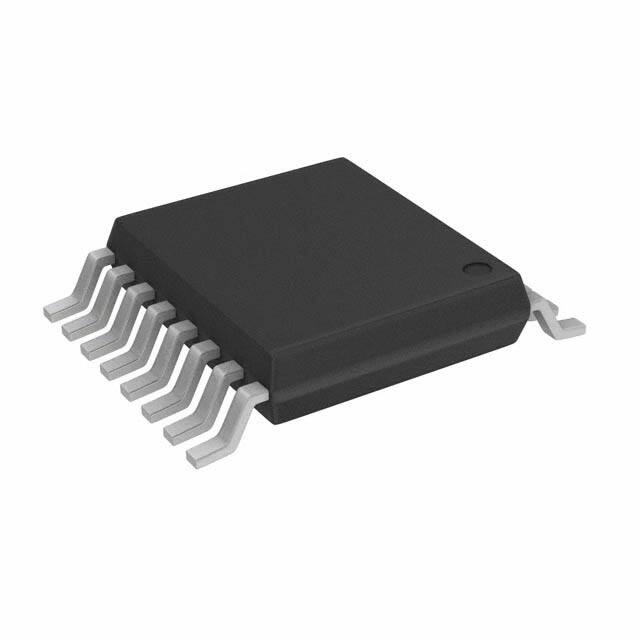
Packaged as 16-pin TSSOP
Eight addressable registers
Replaces multiple crystals and oscillators
Output frequencies up to 200 MHz at 3.3 V
Configurable Spread Spectrum Modulation
Input crystal frequency of 5 to 27 MHz
Input clock frequency of 3 to 166 MHz
Up to three reference outputs
Operating voltages of 3.3 V
VDDO output control from 1.8 V to 3.3 V
Controllable output drive levels
Advanced, low-power CMOS process
Available in Pb (lead) free packaging
NOTE: EOL for non-green parts to occur on 5/13/10
per PDN U-09-01
The ICS281 is also available in factory programmed custom
versions for high-volume applications.
Block Diagram
VDD
S2:S0
3
OTP
ROM
with PLL
Values
Crystal or
clock input
3
VDDO
PLL1 with
Spread
Spectrum
Divide
Logic
and
Output
Enable
Control
PLL2
PLL3
CLK1
CLK2
CLK3
X1/ICLK
Crystal
Oscillator
X2
External capacitors
are required with a crystal input.
GND
3
PDTS
IDT™ / ICS™ TRIPLE PLL FIELD PROG. SPREAD SPECTRUM CLOCK SYNTHESIZER 1
ICS281
REV E 083109
�ICS281
TRIPLE PLL FIELD PROG. SPREAD SPECTRUM CLOCK SYNTHESIZER
EPROM CLOCK SYNTHESIZER
Pin Assignment
GND
16
S2
2
15
3
14
VDD
4
13
VDD
PDTS
GND
VDDO
CLK1
5
6
12
11
CLK2
GND
7
10
VDD
X1/ICLK
8
9
S0
S1
1
CLK3
X2
16 pin (173 mil) TSSOP
Pin Descriptions
Pin
Number
Pin
Name
Pin
Type
1
GND
Power
Connect to ground.
2
S0
Input
Select pin 0. Internal pull-up resistor.
Select pin 1. Internal pull-up resistor.
Connect to +3.3 V.
Pin Description
3
S1
Input
4
VDD
Power
5
VDDO
Power
Power supply for outputs.
6
CLK1
Output
Output clock 1. Weak internal pull-down when tri-state.
7
GND
Power
Connect to ground.
8
X1
XI
Crystal input. Connect this pin to a crystal or external input clock.
9
X2
XO
10
VDD
Power
Crystal Output. Connect this pin to a crystal. Float for clock input.
Connect to +3.3 V.
11
CLK2
Output
Output clock 2. Weak internal pull-down when tri-state.
12
CLK3
Output
Output clock 3. Weak internal pull-down when tri-state.
13
GND
Power
Connect to ground.
14
PDTS
Input
15
VDD
Power
Power-down tri-state. Powers down entire chip and tri-states clock outputs
when low. Internal pull-up resistor.
Connect to +3.3 V.
16
S2
Input
Select pin 2. Internal pull-up resistor.
IDT™ / ICS™ TRIPLE PLL FIELD PROG. SPREAD SPECTRUM CLOCK SYNTHESIZER 2
ICS281
REV E 083109
�ICS281
TRIPLE PLL FIELD PROG. SPREAD SPECTRUM CLOCK SYNTHESIZER
External Components
EPROM CLOCK SYNTHESIZER
The ICS281 requires a minimum number of external
components for proper operation.
The ICS281 also provides separate output divide values,
from 2 through 63, to allow the two output clock banks to
support widely differing frequency values from the same
PLL.
Series Termination Resistor
Each output frequency can be represented as:
Clock output traces over one inch should use series
termination. To series terminate a 50Ω trace (a commonly
used trace impedance), place a 33Ω resistor in series with
the clock line, as close to the clock output pin as possible.
The nominal impedance of the clock output is 20Ω.
Decoupling Capacitors
As with any high-performance mixed-signal IC, the ICS281
must be isolated from system power supply noise to perform
optimally.
OutputFreq
=
REFFreq
⋅
M
----N
Output Drive Control
The ICS281 has two output drive settings. For VDDO=VDD,
low drive should be selected when outputs are less than 100
MHz. High drive should be selected when outputs are
greater than 100 MHz.
Decoupling capacitors of 0.01µF must be connected
between each VDD and the PCB ground plane. For
optimum device performance, the decoupling capacitor
should be mounted on the component side of the PCB.
Avoid the use of vias on the decoupling circuit.
For VDDO
很抱歉,暂时无法提供与“ICS281PG”相匹配的价格&库存,您可以联系我们找货
免费人工找货